Abstract âThe switching speed of a bidirectional microcomputer bus driven by MOS technology drivers is limited by device output characteris- tics. Increasing ...
IEEE JOURNAL OF SOLID-STATE CIRCUITS, VOL. SC-20, NO. 4, AUGUST 1985
828
Regular Papers Negative Capacitance Bus Terminator for Improving the Switching Speed of a Microcomputer Databus M. SHOJI,
SENIOR MEMBER,
IEEE, AND ROBERT
Abstract —The switching speed of a bidirectional microcomputer bus driven by MOS technology drivers is limited by device output characteristics. Increasing the size of the MOS drivers to lower the output resistance leads to a proportional increase in device capacitance. The net effect is no improvement. The data transfer speed of a microcomputer bus can be improved by adding an active circuit to the bus. This active circuit amplifies the bus voltage and feeds back to the bus a current which is proportional to the time rate of change of the bus voltage. This circuit effectively adds a negative capacitance to the bus. The practicaf capacitance canceling capability is limited by the propagation delay time of the operational amplifier in the active circuit. The theory of microcomputer bus structures with negative capacitance including effects of amplifier delay is preseuted. Typically, an operational amplifier with propagation delay less than one tenth of the bus time constant is required to achieve significant (factor of 2) bus speed improvement. High-performance operational amplifiers were used to construct a working model of the negative capacitance bus terminator. The experimental results agreed well with the theory.
I.
INTRODUCTION
I
N ORDER TO IMPROVE performance of a microcom-
puter based on a single-chip microprocessor, the data transfer speed of its databus must be increased. As the microprocessor technology evolves from a simple 8-bit data width machine to a more powerful and complex 16- or 32-bit data width machine, the databus of a microcomputer must communicate with many functional elements of the computer system. Therefore the databus driver must drive a very heavy capacitive load and data transfer speed suffers. Since the data bus is bidirectional, increasing the size of the bus driver on the microprocessor chip does not improve the bus speed, because the driver size of the other bushmasters must also be increased and such a size increase adds more capacitance to the bus.
Manuscript received March 15, 1984; rewsed January 16, 1985. The authors are with AT&T Bell Laboratories, Murray Hill, NJ 07974.
MENUHIN
ROLFE,
SENIOR
MEMBER,
IEEE
A traditional way of solving the driver problem has been to buffer the CPU databus with bipolar (lTL) drivers that have more drive capability than on-chip MOS drivers. The databus is often split into two (a CPU input databus and a CPU output databus), thereby making the driver problem easier. This technique is not attractive for newgeneration microcomputers since the bipolar interface itself requires extra propagation delay which leads to reduced throughput. The problem of bidirectional databus drivers is not limited to a computer system. Some new generation automatic VLSI test machines have a test head that is so complex, large, and heavy, that the test head cannot be brought to the immediate proximity of a CPU chip to be tested. The test head must be connected to the chip by a length of cable, the capacitance of which can be so large that the test may not provide realistic loading specifications. The objective of this paper is to provide a solution to the difficult problem of high capacitance on bidirectional buses. The new approach described here assumes that a bidirectional bus need not be a passive pair of wires, but can also have an active terminating device which can help the busmaster drive the bus quickly. In the simplest configuration the active bus terminator may have a circuit such as that shown in Fig. l(a). Since voltage V and current 1 satisfies
I=co$+&ov-v)=
{CO–(PO–l)C1}$ (1)
the active terminator and the bus (with capacitance Co) looks like a single capacitance Cz = CO– C1(pO – 1). If PO >1, then C2 < Co: the active terminator is effectively presenting a negative capacitance to the bus that partially cancels out the positive bus capacitance. Since the bus
0018-9200/85 /0800-0828 $01.00@1985IEEE
SHOIJIAND ROLFE:BUS TERMINATORFOR IMPROVING SWITCHING SPEED
whose coefficient is proportional to the delay emerges in the basic equation. In the following analysis the delay of the amplifier is characterized by the circuit of Fig. l(b), where an idealized amplifier that has no delay reqeives i& input signal through a delay line. The output voltage VO(t) is related to the input voltage V(t) by
(t)
AMPLIFIER
CNARACTERIZATION
Vo(t)=pol’’(t-to)
(2)
(a)
where rO is the delay constant of the delay line and p o is the gain of the amplifier. Referring to Fig. l(a) and assuming that the ,,amplifier is described by the model Fig. l(b) the basic circuit equation reads
“)”’*”t) to (b)
COWLEX
~ ~= 0 dt
S-PLAt& s~
(3)
where R o is the internal resistance of the driver of the busmaster. When the driver consists of P- and NFET’s of 2.5-pm CMOS technology, the minimum channel resistance of an FET is in a range of 30–300 0 [4]. Since an FET is a nonlinear gate-voltage-dependent device, effective resistance of the device to a capacitive load is about 6 times the minimum channel resistance. Voltages VO(t] and V are related by (2). From (2) and (3)
0.0.
lr#3?EAslNG b C.D]
14+n
IQ’P:
+Cl${vo(t)–v}
R.
t
I
po’,pm
~1(~)–J”
(c) Fig. 1. (a) Negative capacitance bus terminator. (b) Model of an amplifler that has delay r.. (c) Naturaf frequency S versus amplifier gain p..
Vi(t)–v
dV
z= drivers see smaller capacitance, the bus switching speed becomes faster. This is a technique of pole-zero compensation in linear operational amplifier technology [1]. The concept of a negative capacitance bus terminator includes the application of linear operational amplifier technology to digital circuits, but it is substantially more than that. Classical analysis of operational amplifiers [2] and active filters [3] are frequency-domain analysis. These results are inconvenient for us, since we are interested in delay times. Therefore we developed a concise time-domain analysis. The analysis of (1) is valid when the amplifier delay is negligible compared with the RC time constant R OCOof Fig. l(a). When the amplifier has a delay, the terminator does not present a pure capacitance, and the problem becomes complex. This problem will be discussed in the next section.
RO(CO+C1)
c1 +
co+q
Po&(t
Equation (4) is a functional-differential equation that is difficult to solve. The difficulty arises from the last term that refers not to time t,but to time t– to. As a first step toward understanding the problem one may assume that to is small. Then by utilizing
$v(t–to)=~
dV(t ) _tod2v(t) — dt 2
one obtains c
~otod’v(t) dt’
1
dV( t )
+{co+cl(l–po)}~ +
v(t) = RO
II.
THEORY
OF NEGATIVE
CAPACITANCE
Bus
TERMINATOR
Signal propagation delays through the amplifier play a crucial role in determining the, characteristics of the negative capacitance bus terminator of Fig. l(a). If the delay is zero, the basic circuit equation includes only up to the first-order derivative of the voltages with time, as in (1) of the last section. It will be shown that, if the delay is small but is not zero, the time derivative of the second order
(4)
-to)’
Vi(t) — RO
“
(5)
From (5) one observes that the amplifier delay creates a term that is a higher order derivative of time. By assuming V a e ‘t in the homogeneous part of (5) (the left-hand side of the equal sign set equal to zero), the natural frequency of the circuit S satisfies the following secular equation:
clpotos* + {c. + Cl(l–po)}s+
+ =0 o
(6)
830
IEEE JOURNAL OF SOLID-STATE CIRCUITS, VOL sC-20,
NO. 4, AUGUST 1985
which is solved as
s+= —
2C:P0,0
F
W-PO)}*W
{co+
(7)
where
),
=C:(po–p+)(po–p. and where ~+=1+++3
CIRO +
1
/(
co
to
4C1R0
‘ L——l_—_
to
1+ ~+
CIRO –)
“
“o
01
02
0.3
0.4
AMPLIFIER
OELAY
05
tO/ROCO
If to were zero, the bus capacitance nulls when the amplifier gain is pc, where PC is given by
(8)
pc=l+:. 1
It can be shown that p+> PC > p _. By utilizing these quantities (7) becomes
s+=sR(po)*s,(po)
NORMALIZED
Fig. 2.
Switching
time improvement factor versus normalized delay for severaf values of Cl/CO.
amplifier
By utilizing S+—and
V,(t)=o,
fort0,
and
(9)
the solution of (5) is given by
where
S+es.
PO–PC
SR(I-JO) =
s
(PO)=
I
and
Ztopo
v(t)=l–
/(P+-
2topo
s+
=l–(l–
Po)(P--lJo)
“
When v+> MO> p_, SI(PO) is imaginary. The absolute value of S1( p o) in this case is given by
~s+t
t–s –
s:
Sot)esOr,
when S.=
S+=S.
( =S~(po)).
(10)
where S+, S_ and So are given by (9). The switching time of the bus is defined as the time when the voltage reaches 0.5, and the time can be calculated by solving an implicit equation, V(t)= 0.5, for t.It is A(po)=lsl(po)y= IJO(P++ I-–)-P+ P--)4 helpful to compare the switching time of the uncom(2to)2p: “ pensated bus with the switching time of the bus compensated up to the critical damping point. The ratio is This function has a maximum at plotted versus the amplifier delay to (normalized to the 2p+p_ Pc time constant of the bus R OCO), for several values of 0 an instabilityy occurs. improvement in bus switching time, the delay time of the The real-time voltage response of the system (in the stable amplifier must be less than 0.1 times the bus time constant. regime) can be classified into the case of overdamping The amplifier model shown in Fig. l(b) is too simple to (0.D. in the figure), critical damping (C.D.) and under- represent a real operational amplifier. A more realistic, damping (U.D.), as shown in Fig. l(c). two-stage amplifier model was used instead of (2) and the
SHOIJ1 AND ROLFE: BUS TERMINATOR
FOR IMPROVING SWITCHING
831
SPEED
A.WJ
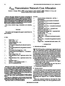
Fig.
I 0. t
l) o NORMALIZED
5.
Detailed
I 0.2
AMPLIFIER
circuit schematic of the negative used for experimental verification.
capacitance
circuit
TABLE I COMPARISONOF THEORY TO EXPERIMENT
DELAY
bl~co
Fig. 3. Amplifier gain at critical damping versus normalized amplifier delay for several values of the switching speed improvement factor K.
n
.
Pf
C“c’
t+ —sJu_ ~c,
I&
100
4s
049
!3.55 + .22 -o
500
55
0.60
0.11 + W -o
1.27
1000
70
0.77
0.0s +’ .02 –o
I 23
S&
SR,W
0.66
2
1
1
0.75
0.67
0.76
0.$7
045
0.5s
Note: SR is the ratio of switching time of the circuit with capacitance canceling to the situation without capacitance canceling. The theoretical ratio is evaluated at criticaf damping where the gain is p_.
WITHOUT
C - CAtWE1-LKTKIN
I
wITH C- CANCELLATION I
I
oo~ NORMALIZED
Tlf&
(t/%
TIME [NANOSECONDS)
Co)
TIME
Fig. 4. Reaf-time bus response for severaf values of amplifier gain. A two-stage amplifier whose first and the second stages have delay 0.025 R ~Co (where ROCO is the bus time constant) was assumed in the analysis.
problem was solved by a computer. Fig. 4 shows a set of results. As the gain of the amplifier is increased the bus response changes from the overdamping to the critical damping, and then to the underdamping. The underdamped bus is fast but practically undesirable because of the overshoot. The numerical analysis showed that a diode clipper can be incorporated into the bus to suppress the overshoot within a certain limit.
III.
PRACTICAL
IMPLEMENTATION
OF THE NEGATIVE
CAPACITOR
The principal component of the negative capacitor is the fast operational amplifier such as the MSK-880 operational amplifier manufactured by M. S. Kennedy Company, Syracuse, New York. When p.= 2, the 50-percent point of
(NANOSECONDS)
7opf
SW17CHING TIWE * 103NS
Fig. 6.
SWITCHffi
TIME =45NS
Demonstration of switching time improvement by a negative capacitance (for RO = 10000, Co =91 pf).
the output waveform is delayed approximately 5 ns from the 50-percent point of input waveform. Fig. 5 shows the actual circuit used to demonstrate the pulse performance of the negative capacitor. Values of the series resistance R ~ were chosen to simulate typical CMOS device of 2.5-pm feature size. The bus capacitance CO is compensated by the negative capacitance created by the operational amplifier and Cl. Table I shows some results from the circuit of Fig. 6 and some other experimental results compared to the theoretical result for pulse rise-time
832
IEEE JOURNAL
improvements. Table I indicates that the factor of improvement observed experimentally, SR .Xp and that derived from the theory, SR ~heOvagree reasonably well. The real negative capacitor exceeded theoretical expectations because the gain p ~ was fixed at p ~ = 2, and Cl was adjusted for fastest rise time on V(t) with no appreciable overshoot. In this experiment there are some difficulties in determining the critical damping condition. Reduction in bus transfer time achieved in our experiment (67–45 percent) is quite significant. Throughput of a computer can be improved by a factor of two by a negative capacitance btis terminator, if bus transfer time limits the speed of the computer. As a computer becomes complex, bus transfer time becomes the most serious speed-limiting mechanism.
IV.
DISCUSSION
A negative capacitance bus terminator presents a negative capacitance to the bus at all times. The negative capacitance is produced by a fast linear amplifier which, unfortunately, consumes relatively high standby power. In order to improve the bus switching time, it is sufficient that the terminator presents a negative capacitance only when the bus changes state. If the negative capacitance circuit is turned off when the bus stays in one state, high standby power can be avoided. A negative capacitance bus terminator can solve the difficult problem of interfacing an MOS microprocessor directly to a large memory array. When the access time of the MOS memory is reduced to the 50-ns range, buffering the processor output by bipolar IC’S becomes less effective since the delay time through the buffer itself becomes significant. A negative capacitance bus terminator then becomes a practical method of solving the interfacing problems of MOS VLSI processor systems. This situation is expected to arise when the clock frequency of processors exceeds 10 MHz. Traditionally, a computer bus has been a bundle of metal wires that served as a medium for data exchange. If the bus is made an active device, a significant performance improvement of the computer system is expected. The concept of a negative capacitance bus terminator may lead to a new microcomputer architecture, since the internal databus of the processor can be directly connected to the external computer bus with a negative capacitance bus terminator.
OF SOLID-STATE CIRCUITS,VOL. SC-20, NO. 4, AUGUST 1985
ACKNOWLEDGMENT
The authors wish to acknowledge R. H. Krambeck and M. R. Barber for their helpful discussions and encouragement. They wish to thank B. T. Murphy for valuable comments on the manuscript.
REFERENCES [1] [2] [3] [4]
J. G. Graeme, “Application of operational amplifiers, third generation techniques,” Burr Brown Res. Corp., Tech. Rep., 1973. J. K. Roberge, OperationalA mpl~iers. New York: Wiley, 1975. EL Y-F Lam, Analog and Digital Filters: Design and Realization. Englewood Cliffs, NJ, Prentice-Hall, 1979. A typicaJ design is reported in M. Shoji, “Electrical design of BellMac 32A microprocessor;” in Proc. ICCC 82 Dig., Sept. 1982, pp. 112-115.
M. Shoji (M67–SM’70) was born in Tokyo, Japan, on January 13,1936. He received the B.SC degree from the University of Tokyo in 1958, and the Ph.D degree from the University of Minnesota, Minneapolis, MN, in 1965. He received the SC.D degree from the University of Tokyo, Tokyo, Japan, in 1971. He joined Bell Telephone Laboratones, Murray Hill, NJ, in 1965 and was initially engaged in the research of the transferred electron phenomena. Later he worked on mametic bubble devices and linear integrated circuits. From 1976 to the pres;nt he worked in the project of CMOS microprocessors, and was a senior member of the design team of the BellMac 32 series CPU’S. He is presently a member of the Computing Science Research Center of AT&T Bell Laboratories, Murray Hill, NJ.
Robert Memrhin Rolfe (M80–SM83) received the B. S., M. S., and Ph.D. degrees from University of California, Los Angeles. He was a Technical Group Supervisor at AT&T Bell Laboratories until 1983 where he was responsible for the VLSI Module Design Req~rements and Certification Group for the BELLMAC 32 microprocessor product line. He also served as the technical group supervisor for the Physical Design Group for Bellmac Microprocessors and Microprocessor Development Systems product line. He is currently Principal Engineer in the VHSIC Operation of Harris Corporation VHSIC Government Systems Sector in Melbourne, FL. His responsibilities include development of architectural concepts for VHSIC support technologies inchiding integrated design automation systems (IDAS), automatic test generation systems, and VHSIC packaging technology. He presently is Technical Director of the Harris Corporation Tester Independent Software Support System (TISSS) Program to develop a fully automatic test program generation system for military integrritcd circuits. Dr. Rolfe is inventor and coinventor for two US patents in digital and analog circuit design. He has 12 technical publications in a number of technical areas including electromagnetic, high-energy nuclear physics, and VLSI development.