Jul 31, 2014 - display and 32 Gb SHDC SD memory card). The sample rate is con- figurable up ... one of the many Arduino shields available off-the-shelf or dedicated ... ence of the custom programmable dual SPI/I2C interface which can be.
Open platform, 32-channel, portable, data-logger with 32 PGA control lines for wearable medical device development G.D. Gargiulo, P. Bifulco, M. Cesarelli, A. McEwan and A. Wabnitz A compact isolated low-power 32-channel 16-bit data-logging system around an NXP ARM processor (LPC1768) and four of the linear technology octal analogue-to-digital converters (ADCs) LTC1857/58/59 is designed. The system requires only 250 mA when powered at 5 V to run at full power (including a capacitive 2.8 inch touch-screen display and 32 Gb SHDC SD memory card). The sample rate is configurable up to 1 k SPS per channel as well as voltage dynamic input up to ±10 V; additionally, 32 chip select lines (SPI protocol) individually addressable and controllable while sampling to configure userdesigned programmable gain amplifiers (PGAs) are available. Collaboration is being sought to improve the software capabilities, particularly to enrich the very basic user interface and to add wireless connectivity. The code is available (under the GPL licence) at our repository, the gerber file to reproduce the PCB is available (on the As-Is basis) on request. The galvanic isolation between the power supply data connection and ADC channels makes the data-logger also compatible with the main powered PCs, hence it is suitable for the implementation of medical devices at least for the prototyping and initial testing stages.
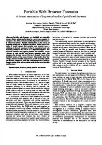
2.8 inch capacitive touch-screen and the memory card slot (on the bottom side, not visible in the Figure). The evaluation kit also can be purchased in a bundle with a standard J-tag cable programmer/debugger suitable for KEIL and for other programming environments. On the board are present a ‘root’ and ‘device’ universal serial bus (USB) connection as well as a local area network (LAN) port and four user buttons. Currently, since the device is intended to be part of a wearable system, we do not use the LAN connection. USER
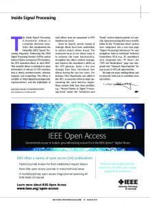
ARM board GUI
touch-screen display 5 V power supply (Li-ion rechargeable battery pack)
ARM CPU (LPC1768)
USB-host driver
mass storage (SD card)
• 32x PGA CS lines (SPI) • 32x analogue channels • USER available isolated power supply (3.3 V max 200 mA; 5 V max 500 mA)
ADCs driver (PIC18F46J50 USB device)
isolated USB/power ADC board
Fig. 1 Hardware architecture block diagram
Introduction: Bio-potential signals such as electrocardiogram (ECG), electroencephalogram and electromyogram are extensively used in clinical practice to assess the physical condition and health status of patients [1]. Although the diagnosis of diseases is carried out in hospitals or clinical environments by expert practitioners, there is a modern trend of non-invasive, unobtrusive and long-lasting patient’s monitoring outside the clinical environment, particularly performed in the comfort of the subject’s home [2, 3]. For approved medical devices, particularly for ECG monitoring, longterm monitoring data-logging is performed employing Holter devices [4]. However, designers developing new medical devices, particularly where the focus is on the capability of recording electrophysiological signals continuously, with no (or very little) subject preparation/supervision (i.e. sleep studies) and with dry electrodes [5–7], face problems of a lack of a flexible Holter monitor-style device capable of: 1. recording for 24 h or more on a standard mass memory device; 2. safe and insulated connection between the subject and an analogue bio-potential amplifier; and 3. easy to use/also usable in hospital environments (at least for research trials). Currently, designers not willing to implement a wireless solution have to implement their own data-logging circuitry [8] based on standardised guidelines, for example, projects [9]. Alternatively, designers may adapt one of the many Arduino shields available off-the-shelf or dedicated acquisition hardware [10, 11]. Unfortunately, these solutions have a limited number of channels, limited sample rate capability or are designed for a specific bio-signal (i.e. 12-lead ECG). The aim of our project is to make available an open source hardware/software platform that, apart from addressing the above requirements, supports dynamically programmable gain amplifiers (PGAs) hence allowing much greater flexibility and usability for hospital environments or research trials on BCI, fetal monitoring and ECG monitoring [6, 7, 12–15]. Methods: To make our hardware flexible, reusable and easy to use and clean, we decided to implement the user interface entirely on a touch-screen display. Moreover, to contain the hardware development costs, we decided to use one of the numerous readily available off-the-shelf ARM processors with display evaluation kits. This allowed us to focus our design effort solely on the isolated data acquisition board that can be used also with a standard PC. Therefore, our hardware architecture (depicted in Fig. 1) is divided into two boards. One board hosts the processor, the touch-screen display, the memory card and the support circuitry for the processor to function. From the plethora of those available, we selected a development board for LPC1768 by Thaoyu Electronics (http://www. powermcu.com). The evaluation kit (visible in Fig. 2) includes a
Fig. 2 ARM processor board connected to ADC board running user interface on 2.8 inch touch-screen monitor
The second board (the isolated data acquisition board) is a custom board designed to fit the assembled board directly under the evaluation kit board to save the overall package area, see Fig.2. At the heart of this board, there is a supporting processor (PIC18F46J50). This PIC was selected because of the presence of the USB interface and for the presence of the custom programmable dual SPI/I2C interface which can be used to control (as in our case) four SPI analogue-to-digital converters (ADCs) and a number of SPI digital potentiometers or directly PGAs. The use of the PIC as the USB device allowed us to simplify the galvanic insulation interface that uses a standard USB galvanic insulator (ADuM4160). As an additional benefit, a PC driver is available to allow testing and use of the data acquisition board with a PC or different processor. As mentioned, our system includes four ADCs (LTC1857/58/59) which share the data lines for their SPI interface, but use individual control lines to flag a ‘busy’ state or to command the ‘start of conversion’. An anti-aliasing filter is achieved by a small capacitor connected in parallel to each of the analogue channel inputs. Its value (in our supplied schematic configured for a sample rate of 1000 SPS) can be calculated in accordance with the desired sample rate and the ADC input impedance. To complete the board design, we designed a fully isolated power supply employing the chip ADuM5000W for both analogue and digital 5 V as well as the auxiliary 3.3 V digital power output. Owing to the presence of two separate processors, two sets of firmware software are required. The ARM firmware is programmed in such a way that at start-up it loads directly to the user interface as
ELECTRONICS LETTERS 31st July 2014 Vol. 50 No. 16 pp. 1127–1129
depicted in Fig. 2. The boot time is < 2 s and the device will wait indefinitely for user actions. The user interface is also a real-time diagnostic for the device as it displays the device status such as: (i) current date and time (from the on board real-time clock; (ii) presence and available space on the SD card; (iii) presence and status of acquisition board and (iv) current ‘patient ID’ is also displayed together with the current sample rate. The PIC firmware instead is programmed as the USB device. At the start-up, it enters in idle mode waiting for commands to start data acquisition and assertion of value for the PGA gains. Results: The PCB that we implemented to provide room for the PIC, ADCs, the isolated interface and the PGA gain control circuitry is depicted in Fig. 3 (limited to the top layer and components outline). In the Figure are also highlighted the position of the ADCs, the PGAs’ chip-select connections, the isolator area (evident from the empty copper area) and the bottom mounting holes that are positioned to match the ARM processor PCB ones. As it is possible to infer from Fig. 1, the total size of the data-logger is