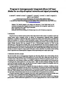
Optical signal processing using SOAs for packet switching H. Avramopoulos National Technical University of Athens – School of Electrical Engineering and Computer Science 9 Iroon Polytechniou Street, Zografou 15773 –Athens, Greece Tel. +30-210-772 2057, Fax +30-210-7722077, Email:
[email protected]
Abstract: We discuss the use of SOA-based interferometric gates for optical packet switching applications. Based on these modules, key signal processing functionalities required by a packet switched node are demonstrated directly in the optical domain. 2003 Optical Society of America
OCIS codes: (250.5980) Semiconductor Optical Amplifiers; (070.4560) Optical data processing; (050.2230) Fabry-Perot
1. Introduction Optical packet switching has been introduced as the main concept to efficiently utilize the large transmission capacity offered by fiber-based technology, as it aims to combine the speed advantages of optical signal processing techniques and the benefits in terms of flexibility, granularity and on-demand use of bandwidth provided by packet switched networks [1]. However, the realization of optical packet switched networks is certainly a demanding technological challenge. Key network node functionalities have to be performed directly in the optical domain and the optical subsystems are required to successfully and “on the fly” process the inherently packet-formatted traffic on a packet-by-packet basis. The challenge becomes even more pronounced when packet-format transparent processing is targeted. In this case, asynchronous, variable-length or even bursty optical packets comprise the data traffic, imposing the additional requirement for the intra-node optical signal processing subsystems to handle with the incoming information irrespective of the precise packet phase alignment, packet duration or packet-to-packet power level fluctuation, respectively. Towards the effort for all-optical implementation of the key signal processing subsystems required by a packet switched node, emphasis should be given on exploiting the advantages provided by Semiconductor Optical Amplifier (SOA)-based switching technology. SOA-based optical gates possess high-speed bitwise processing capabilities [2] due to their ultra-fast response to external light injection, making them suitable to perform successfully even with asynchronous or variable-length optical packets. Moreover, their strong non-linear characteristics, especially when operating in the deeply saturated regime, are ideally suitable for power level equalization purposes required in the case of optical bursts with strong packet-to-packet power fluctuations. These properties in combination with the remarkable progress of semiconductor-based technology that has been made during the last years in terms of integration potential [2], operational speed [3] and variety of functional signal processing applications [4-7], imply that SOA-based switches can form a promising and viable platform for the basis of future optical packet switched networks. In this article, we provide experimental proof of the above argumentation and present some indicative, recent research results at 10 Gb/s regarding the implementation of key intra-node packet switching functionalities using SOA-based optical gates. 2. SOA-based processing modules for packet switching The intra-node signal processing subsystems required by a true all-optical packet switch, as well as the evolution of the incoming data packet traffic through the node stages for one incoming link are illustrated in the generic packet switched node block diagram shown in Fig. 1. At the front-stage of the node, a clock recovery unit is responsible for extracting the timing information of the optical packet and providing a packet clock signal required for
Fig. 1. Block diagram of a generic packet switched node.
Fig. 2. Block diagrams of the (a) Packet Clock Recovery Circuit and (b) Optically Addressable Exchange/Bypass Packet Switch. Time base on oscilloscope traces is 500 ps/div. The insets describe the respective simplified experimental setups. PBS: Polarization Beam Splitter, SOA: Semiconductor Optical Amplifier, PM Fiber: Polarization Maintaining Fiber.
separated from the packet payload in a header extraction module and the extracted header is launched into a header processing unit, whereas the headerless payload enters the header reinsertion subsystem. The role of the header processing unit is to recognize and identify the desired packet destination and to generate the control signals for properly driving the switching matrix elements. Moreover, the header processing unit generates the new packet address information that enters the header reinsertion module in order to be placed at the front of the packet payload for determining its remaining route into the network. After the new header has been assigned to the payload, the packet is inserted into the switching matrix. This matrix consists of a number of 2x2 controllable switching elements, dedicated to guide the incoming packet to the desired outgoing link when properly driven by the control signals originating from the header processing unit. At every outgoing link, a 3R Regeneration stage is incorporated to restore signal quality and ensure errorless transmission until the next optical node. Fig. 2(a) and 2(b) show the block diagrams of a recently demonstrated packet clock recovery circuit [8] and a 2x2 optically addressable exchange/bypass packet switch [9], respectively, as well as their principle of operation. The packet clock recovery circuit consists of a low-finesse Fabry-Perot filter (FPF) with a Free Spectral Range (FSR) equal to the data line-rate, and an Ultrafast Nonlinear Interferometer (UNI) powered by a strong CW signal. The role of the low-finesse Fabry-Perot filter is to fill the ‘0’s of the incoming optical packet with amplitude modulated clock pulses, providing this way at its output a packet clock resembling signal with strong amplitude modulation. By applying this signal as the control signal into the optical gate that operates in the deeply saturated regime by means of the CW signal, amplitude equalization between the clock pulses is achieved and a packet clock signal with a few bits rise time and duration similar to that of the original data packet is imprinted on the CW signal. To this end, clock extraction on a packet-by-packet basis requiring just a few bits as guardbands becomes possible, even for asynchronous data packets. Performance analysis of the recovered clock signal in terms of jitter also proves its suitability for packet regeneration or packet reception purposes. The enhanced power fluctuation suppression properties of the gate owe to its hard-limiting behavior when the SOA operates in the saturated regime [10], also indicating that optical gates acting as hard-limiters can be used for power equalization purposes when burst-mode traffic is considered [11]. The 2x2 packet switch illustrated in Fig. 2(b) comprises of a UNI gate, specially configured so as to have 2 inputs and 2 outputs, as shown in the inset of the same figure. When no control signal is applied, the switch operates in the BAR state and the two incoming data streams remain unaffected and leave the gate from its two output ports. When a control signal is present, the switch operates in the CROSS state and the content of the two incoming data signals that falls within the switching window of the control signal is exchanged. The dashed line in the oscilloscope traces of fig. 2(b) indicates the control signal duration as well as the corresponding data content that is exchanged, while it can be easily seen that the information of the data signals outside the dashed line simply passes through the BAR-state operating switch. Such optically controllable 2x2 packet switches with high-speed, bit-level operational capabilities are particularly desirable as the basic elements for constructing a whole switching matrix. Although the two circuits shown in fig. 2 have been described in terms of their own functionality, these two modules constitute the essential units required to implement a variety of signal processing functionalities needed within a packet switched node. An indicative example of their potential is a header separation and reinsertion module that is shown in fig. 3. It consists of a packet clock extraction circuit which is followed by a 2x2
Fig. 3. Block diagram of the Header Separation and Reinsertion Module. Time base on oscilloscope traces is 500 ps/div.
exchange/bypass switch. Part of the data packet signal is inserted into the clock recovery module, and the obtained packet clock signal is used as the control signal into the 2x2 switch. The remaining part of the data packet signal enters the 2x2 switch via one of its input ports and is synchronized in a way that only the payload bits of the data packet fall within the switching window of the control signal. In this way, the switch operates in the CROSS state only for the duration of the payload section, while for the address information section the switch operates in the BAR state. To this end, successful address/payload separation is achieved [12]. The same unit can be used for new header reinsertion by simply launching the new header as the second input signal into the switch, synchronized with the header section of the original data packet [13]. The new header will simply pass through the BAR-state operating switch and will be placed at the front of the switched payload section, whereas the old header emerges at the other output port of the gate, as also illustrated in the switch output oscilloscope traces of fig.3. The clock recovery unit and the 2x2 packet switch can be also used for the implementation of circuits for 3R regeneration and for Clock-and-Data Recovery purposes for asynchronous optical packets [14], as well as for optical high-speed burst-mode receivers [11]. As such, almost all of the packet switched node key functionalities depicted in fig.1 except header processing can be realized based on these two modules [15]. However, it should be mentioned that research efforts on semiconductor-based devices have already lead to the development of critical submodules even for header processing purposes, like optical flip-flops [16] and control signal generation circuits [17]. 3. Conclusion We have briefly described recent research work on SOA-based optical gates for packet switching applications. We have provided experimental evidence of their potential to operate on a packet-by-packet basis with very low guardband requirements and provide solutions even for asynchronous and burst-mode traffic. The maturation of SOA-based switching technology in terms of integration and speed characteristics [18] suggests that these circuits can be used for the implementation of a compact, true all-optical packet switch at line rates beyond 10 Gb/s. References 1. 2. 3. 4. 5. 6. 7. 8. 9. 10. 11. 12. 13. 14. 15. 16. 17. 18.
D. J. Blumenthal et al, IEEE Commun. Mag. 41, S23-S29 (2003). R. P. Webb, R. J. Manning, G. D. Maxwell, and A. J. Poustie, Electron. Lett. 39, pp. 79-81 (2003). S. A. Hamilton, B. S. Robinson, T. E. Murphy, S. J. Savage, and E. P. Ippen, IEEE/OSA J. Lightwave Technol. 20, 2086 -2100 (2002). B. Sartorius, in ECOC 2001, Vol. 5, pp. 98-125. M. Tsurusawa, K. Nishimura, and M. Usami, in ECOC 2001, Vol. 4, pp. 500-501. S. Nakamura, Y. Ueno, and K. Tajima, IEEE Photon. Technol. Lett. 13, 1091-1093 (2001). H. J. S. Dorren et al, IEEE/OSA J. Lightwave Technol. 21, 2 -12 (2003). N. Pleros et al, IEEE Photon. Technol. Lett. 15, 1291-1293 (2003). G. Theophilopoulos et al, IEEE Photon. Technol. Lett. 14, 998-1000 (2002). G. T. Kanellos et al, submitted to OAA/IPR 2004. E. Kehayas et al, submitted to IEEE/OSA J. Lightwave. Technol., Special Issue on Metro & Access Networks. C. Bintjas et al, IEEE Photon. Technol. Lett. 14, 1728-1730 (2002). D. Tsiokos, E. Kehayas, G.T. Kanellos, L. Stampoulidis, G. Guekos, and H. Avramopoulos, in ECOC 2003, We4.P.83. G. T. Kanellos et al, IEEE Photon. Technol. Lett. 15, 1666-1668 (2003). C. Bintjas, K. Vlachos, N. Pleros and H. Avramopoulos, IEEE/OSA J. Lightwave Technol. 21, 2629–2637 (2003). H. J. S. Dorren et al, IEEE J. Quantum Electron, 39, 141 - 148 (2003). L. Stampoulidis et al, submitted to OAA/IPR 2004. T. Akiyama et al., IEEE J. Quantum Electron, 37, 1059-1065 (2001).