PSP-based scalable compact FinFET model. G.D.J. Smit1, A.J. Scholten1, G. Curatola2, R. van Langevelde3, G. Gildenblat4, and D.B.M. Klaassen1.
PSP-based scalable compact FinFET model G.D.J. Smit1 , A.J. Scholten1 , G. Curatola2 , R. van Langevelde3 , G. Gildenblat4 , and D.B.M. Klaassen1 1 NXP
Semiconductors Research, High Tech Campus 5, 5656 AE Eindhoven, The Netherlands — 2 NXP Semiconductors Research, Leuven 3 Philips Research Europe, Eindhoven, The Netherlands — 4 Arizona State University, Tempe AZ, USA
(Invited) ABSTRACT A high-quality compact FinFET model is a prerequisite for initial circuit design and evaluation of these prospective replacements for conventional bulk MOSFETs in real circuits. Our PSP-based compact model for symmetric 3-terminal FinFETs with thin undoped or lightly doped body contains simple analytical expressions for currents and charges. This makes the model well suited for such circuit simulations. Yet, this surface potential based model offers an accurate description of not only the currents, but also of the (trans-)conductance and capacitances and is continuous over all operating conditions (subthreshold, linear, saturation). The model is fully scalable and will be demonstrated to describe a full range of device geometries, from the longchannel limit down to the shortest channels, with a single set of parameters.
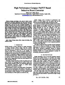
G
tox S
FinFETs are generally seen as prospective replacements for conventional bulk MOSFETs owing to their superior control of short-channel effects (SCEs). They present, however, a serious challenge for compact model development, e.g., due to the different electrostatics. Recently, we presented a new surface potential based compact model for symmetric 3-terminal FinFETs with thin undoped or lightly doped body [1]. It is a complete compact model including SCEs, mobility reduction, and quantum mechanical (QM) corrections, based on well-established techniques from the PSP model [2],[3]. The model describes both currents and charges and is continuous over all operating conditions (subthreshold, linear, saturation). The model has a hierarchical structure (similar to that of the PSP-model [2]), in which the above features are handled at the ‘local’ model level. An essential requirement of a compact model is its ability to give a description of device properties as a continuous function of the device geometry. In case of FinFETs, the channel length L is usually the only design parameter (the fin thickness and fin height are fixed by the technology). The L-scaling properties of the model are handled at the ‘global’ model level. In this paper, we will first give a description of the model core (that is, the core of the local model) in much more de-
520
y = tSi/2 D
x y = −tSi/2 G
x=0
x=L
Figure 1: Schematic of device cross section (parallel to wafer), indicating dimensions, coordinate system, and terminal connections.
tail than in [1]. In the second part, we will extend the work in [1] by focussing on the global model level and treating the scaling-behavior (channel length dependence) of the model.
2
Keywords: FinFET, compact model, PSP, CMOS, scaling
1 INTRODUCTION
y
2.1
MODEL CORE
Conventional approach
We consider a symmetric FinFET with undoped (or lightly doped) body (see Fig. 1). Moreover, we consider a section from an infinitely high fin, i.e., edge-effects due to the top-gate and the buried oxide are neglected. We start by formulating the general theory along the same lines as, e.g., in [4]. Adopting the gradual channel approximation, the Poisson equation across the channel can be written as d2 ψ exp(ψ − v) = , dy2 2
(1)
where ψ(x, y) is the electrostatic potential and v(x) the quasiFermi level of the electrons (also known as the ‘channel potential’). It is convenient to express all voltages (such as ψ, v, and the terminal voltages) in units of ϕT = kB T /e. Similarly, all lengths (suchp as x, y, L) are expressed in units of the Debye length LD = εSi ϕT /(2eNA ), where NA is the equilibrium electron concentration1 . 1 In the context of this paper, the value of N used in the normalization A can be chosen randomly, in principle. It is a matter of convenience to take NA equal to the intrinsic carrier concentration in an undoped fin, or to the doping level in a (lightly) doped fin.
NSTI-Nanotech 2007, www.nsti.org, ISBN 1420061844 Vol. 3, 2007
The general solution of Eq. (1) " # p cos2 ( α(x) · y/2) ψ(x, y) = v(x) − ln α(x)
(2)
contains the integration constant α(x), which must be solved from the boundary condition cox (vG − ψs (x)) = ψ0s (x).
(3)
Here, vG is the gate bias w.r.t. flatband conditions, cox is the capacitance per unit area of the gate dielectric, ψs (x) = ψ(x,tSi /2) is the surface potential, ψ0s (x) = ∂ψ/∂y(x,tSi /2) is the surface electric field, and tSi is the thickness of the silicon body. The local current density in the x-direction is −µ · h · q · dv/dx = −µ · h · (q · dψ/dx − dq/dx) ,
It can be shown that for any solution of the above equations in a symmetric FinFET, θ ∈ (0, π/2). The total drain current can be written, similar to the PaoSah integral [5], as h · L
Z L Z t /2 Si 0
−tSi /2
q(x, y) ·
d v(x) dydx. dx
where ∆Q = QL − Q0 and Q¯ = (Q0 + QL )/2. After having solved α from Eq. (3), this equation gives a complete and explicit description of the drain current in all operating regimes (subthreshold, linear, saturation) for an ideal long channel device. A similar result has been shown before in [4]. Similarly, the charges (required for capacitances) can be calculated. For example, the total inversion charge is given by QI = h ·
(4)
where µ is the mobility and h the height of the fin. The right hand side (i.e., the sum of a drift and a diffusion component) follows directly from adopting the Boltzmann approximation for the local electron charge density q(x, y) = − exp(ψ(x, y) − v(x))/2 by differentiation. Noting that v, α, ψs , and ψ0s depend only on x, while ψ and q depend also on y, the notation will be simplified from now on by dropping the explicit indication of the x- and ydependence. Moreover, it is convenient to introduce √ θ = α · tSi /4 and γ = cox · tSi . (5)
IDS = −µ ·
Finally, the integral over θ can be solved analytically, giving · ¸ ¢ h 4 ¡ 2 1 IDS = 2·µ· · · θL − θ20 + ∆Q − · Q¯ · ∆Q , (11) L tSi 16cox
h · L
Z vL v0
Q dv,
Z t /2 Si −tSi /2
(8)
Here, ψs , and ψ0s were first expressed in terms of θ by using Eq. (2). These results can be used to express the drain current fully in terms of θ, namely Z θL θ0
dv , dx
(13)
dx = −µ ·
h · dv IDS
(14)
the inversion charge can also be expressed in terms of θ as QI = −µ ·
h2 · IDS
Z θL θ0
Q2 ·
dv dθ. dθ
(15)
Again, this integral can be solved in closed form, the result being " h2 QI = −µ · · θ2 − ln(cos2 θ) − 2 · θ · tan θ IDS #θL 4 3 3 + f (θ) − · θ · tan θ , (16) 3·γ θ0
where
q dy = −2 · ψ0s
h · L
(12)
from which it follows that
(7)
is the charge per unit area, which is a function of x. In addition, v0 and vL are shorthand notations for v(0) and v(L). By rewriting the boundary condition Eq. (3), the channel potential v can be expressed as a function of θ as µ 2 ¶ ³t ´ 4 cos θ Si v = vG + ln + 2 · ln − · θ · tan θ. (9) 2 θ 4 γ
IDS = −µ ·
Q dx.
IDS = −µ · h · Q ·
(6)
where Q=
0
Using
Because the channel potential v does not depend on y, the inner integral can be carried out, resulting in IDS = −µ ·
Z L
Q·
dv dθ. dθ
(10)
f (θ) = − −
2·i 3 · θ − ln(2) · θ2 + (1 − θ2 ) · ln cos θ 3
θ2 + θ · tan θ + i · θ · Li2 (−e2·i·θ ) 2 · cos2 θ 3 · ζ(3) 1 − Li3 (−e2·i·θ ) − 2 8
(17)
and Lin (x) is the so-called polylogarithm function. Likewise, the source and drain charges QS and QD (following the WardDutton scheme [6]) can be obtained. The resulting expressions are, however, even more complicated than Eqs. (16) and (17). By comparison to 2D device simulations, it has nevertheless been shown [4] that this leads to a very accurate model for ideal long-channel FinFETs in both the weak and strong inversion regime.
NSTI-Nanotech 2007, www.nsti.org, ISBN 1420061844 Vol. 3, 2007
521
0
10
g(θ)
A major drawback of this approach is the complexity of the expressions for the charges, which involve complex numbers and the usage of special functions. These formulas (though ‘closed form’ expressions) are not suitable for compact modeling purposes, as numerical evaluation of these expressions is non-trivial and time consuming. Moreover, in a compact model, the derivatives of these expressions w.r.t. the terminal voltages are also required, which even adds to the complexity.
−1
10
−2
10
A straightforward but cumbersome computation shows that the remaining integral can be written as q·
dψs dψ dy = Q˜ · , dx dx
(19)
(20)
and g(θ) =
sin(2 · θ) − 2 · θ · cos(2 · θ) . θ · tan(θ) · [2 · θ + sin(2 · θ)]
(21)
Now, we would like to make the approximation Q˜ ≈ Q (corresponding to g(θ) ≈ 0), such that instead of µ ¶ dψs dQ IDS = −µ · h · Q˜ · − . (22) dx dx we can write µ ¶ dψs dQ − IDS = −µ · h · Q · . dx dx
(23)
Below, we will justify that this approximation can indeed be used in our compact model. To this end, first note that in ‘real’ (i.e., non-normalized) units γ = (εox /εSi ) · (tSi /tox ), such that γ/4 ≈ (tSi /tox )/12. For typical devices, γ/4 is roughly equal to 1. The value of g(θ) is plotted in Fig. 2. This graph was created to highlight the limiting behavior of g(θ). It can be
522
0
ψs (in units of ϕT )
40
1.0 0.8
30
0.6 0.4
20
0.2 20 30 40 vG (in units of ϕT )
0.0 50
Figure 3: Plots of g(θ) and ψs as a function of vG . The vertical dashed line roughly indicates the position of the threshold voltage. Above the threshold voltage, g(θ) rapidly drops towards 0.
seen that g(θ) → 2/3 when θ → 0 (corresponding to the subthreshold region). On the other hand
where h i γ Q˜ = Q · 1 + · g(θ) 4
−1
10 10 1 − (2/π ) · θ Figure 2: Plot of g(θ). This plot was created to highlight the limiting behavior of g(θ), when θ approaches the boundaries of its domain.
g(θ)
A new approximation, which we recently proposed [1], leads to a model which (i) is a very good approximation to the ‘exact’ results from the previous section, (ii) coincides with these ‘exact’ result when VDS = 0, (iii) yields much simpler formulas, (iv) allows for easy inclusion of SCEs, and (v) yields no violation of basic symmetry tests. We start by explaining the key idea behind our approach. Integration of Eq. (4) across the channel (i.e., in the ydirection) gives the total channel current, which can be written as µZ t /2 ¶ Si dψ dQ dv q· dy − IDS = −µ·h·Q· = −µ·h· . (18) dx dx dx −tSi /2
−tSi /2
−2
10
2.2 New model
Z t /2 Si
subthreshold → ← strong inversion
g(θ) ≈ 1 −
2 · θ → 0 when θ → π/2 π
(24)
(corresponding to strong inversion). The behavior of g(θ) as a function of gate-bias is shown in Fig. 3. From this, it follows that the approximation Q˜ ≈ Q has a high relative accuracy in strong inversion, where g(θ) rapidly approaches 0 when the gate bias is increased. In the subthreshold region, it is less accurate, but there the resulting error in the drift current is inconsequential as the current is dominated by diffusion. In both cases, the accuracy increases when tSi becomes smaller (i.e., γ decreases). These findings quantitatively justify that we make the approximation Q˜ ≈ Q in our model. The main advantage of this approximation is that using Eq. (23) (instead of Eq. (22)) greatly simplifies performing the required integrals for IDS , QI , QS , and QD . In particular, no polylogarithmic functions are needed. For the drain current, we find µ ¶ dψs dQ dv ≈ −µ · h · Q · − . (25) IDS = −µ · h · Q · dx dx dx From the boundary condition it follows that 2 · cox (ψs − vG ) = Q.
NSTI-Nanotech 2007, www.nsti.org, ISBN 1420061844 Vol. 3, 2007
(26)
IDS = −µ ·
h · Q¯ ∗ · ∆Q∗ , 2 · L · cox
Q¯ ∗ = (Q∗0 + Q∗L )/2,
∆Q∗ = Q∗L − Q∗0 ,
(29)
and Q∗0,L = Q0,L − 2 · cox .
(30)
−QG = QI = Q¯ − η · ∆Q /6,
(32)
η = −∆Q∗ /(2 · Q¯ ∗ ).
(33)
∗
where
Again following the Ward-Dutton charge partitioning scheme [6], expressions for the source- and drain-charge can be obtained along the same lines: £ ¡ ¢ ¤ QD = Q¯ − η + η2 /5 − 1 · ∆Q∗ /6 /2, (34) and
£ ¡ ¢ ¤ QS = Q¯ − η − η2 /5 + 1 · ∆Q∗ /6 /2.
(35)
Indeed, all important quantities have been expressed as simple functions of Q0 and QL . More importantly, the accuracy of the resulting long-channel model is not compromised, as shown in Figs. 4–5. Although Eq. (27) with Q˜ replaced by Q may be reminiscent of the result of the charge-sheet approximation (CSA) commonly used in compact models for conventional MOSFETs, the physical background is completely different. In contrast to CSA, we do not assume that the voltage drop over the inversion layer is negligible. In fact, in our model the physics of the electrostatics in the y-direction is fully preserved, such that the coupling of the two gates and the effect of volume inversion in subthreshold are well accounted for. In this respect, it is good to mention that when VDS → 0 the approximate model approaches the exact results from the previous section. In summary, we have derived equations for the drain current and all terminal charges which are very suitable for compact models and their usage in circuit simulators. The equations are sufficiently simple to allow for efficient numerical evaluation, while on the other hand the accuracy and smoothness of the model are not compromised.
0.0
0.5 1.0 1.5 VGS (V)
gm (arb. units)
0.4
1.0 0.5 0.0
2.0
0.0
0.5 1.0 1.5 VGS (V)
2.0
Figure 4: Direct comparison between ‘exact’ result from Eq. (11) (symbols) and our approximation from Eq. (28) (lines). Drain current (left) and transconductance (right) are shown (tox = 1.2 nm, tSi = 10 nm, and VDS = 10 mV). Note that no fitting parameters are involved in this comparison. Moreover, mobility reduction and series resistance are not included here. 140 120 100 80 60 40 20 0
1032 101 100 10−1 10−2 10−3 10−4 10−5 10−6 10−7 10−8 10
0.0
0.5 1.0 1.5 VGS (V)
2.0
140 120 100 80 60 40 20 0
103 2 10 101 100 10−1 10−2 −3 10 10−4 10−5 10−6
0.0
0.5 1.0 1.5 VGS (V)
gm (arb. units)
which allows for easy integration of Eq. (12) to yield
0.8
ID (arb. units)
The approximation Q˜ ≈ Q is even more advantageous for the charge model. By comparing Eq. (27) and Eq. (28) it follows that dx Q∗ · dQ∗ = ¯∗ , (31) L Q · ∆Q∗
1.2
0.0
(28)
where
1.6
gm (arb. units)
This easily integrates to a simple functions of Q0 and QL :
ID (arb. units)
(27)
gm (arb. units)
µ ¶ h dQ dQ · Q· − 2 · cox . 2 · cox dx dx
101 0 10 10−1 −2 10 10−3 10−4 10−5 −6 10 10−7
1.5 ID (arb. units)
IDS ≈ −µ ·
101 0 10 10−1 10−2 10−3 10−4 10−5 10−6 10−7 10−8
2.0
ID (arb. units)
such that
2.0
Figure 5: Direct comparison between ‘exact’ result from Eq. (11) (symbols) and our approximation from Eq. (28) (lines) at VDS = 1 V. Remaining conditions are the same as in Fig. 4.
2.3
Full local model
Inclusion of SCEs is relatively straightforward in our model. For the symmetric FinFET (after FinFET-specific computation of Q0 and QL ) the expressions for currents and charges (28), (32), (34), and (35) are the same as in the PSP bulk MOSFET model. Consequently, mobility reduction, QM-effects, series resistance, velocity saturation, and channel-length modulation have been integrated in the model in almost exactly the same way as in PSP [2]. As an additional advantage, the parameter sets of this FinFET model and the PSP bulk-MOSFET are very similar. As was already demonstrated in [1], our full model (including SCEs) passes basic symmetry tests for currents (Gummel symmetry) [7] and capacitances [8]. These properties are critical when the model is used in analog/RF circuit simulations.
3 3.1
GEOMETRY SCALING
Parameter extraction
As mentioned before, the FinFET model has a hierarchical structure, similar to the PSP-model [2]. The ‘local model’ describes the characteristics of a device with one particular geometry. This local model contains a complete description of the electrical behavior of this device (currents and capacitances as a function of bias conditions and temperature). Obviously, each local parameter exhibits a clear trend in its behavior as a function of channel length L, for a set of devices from the same technology. This is reflected in the ‘scaling rules’. With each local parameter a (simple) scaling rule is
NSTI-Nanotech 2007, www.nsti.org, ISBN 1420061844 Vol. 3, 2007
523
associated, which describes its behavior as a function of L and is base on physics whenever possible. The free parameters in all scaling rules together constitute the ‘global parameter set’, which is used as input to the global model (that is, the local model plus the scaling rules). The parameter extraction procedure is started by determining local parameter sets for each individual device. Then, the dependency of each local parameter on L can be inspected separately. By adjusting a small number of global parameters (typically two or three), the corresponding scaling rule can be fitted to the extracted local parameter values.
3.2 2D Device simulations To verify the scaling capabilities of the model, we have performed 2D device simulations for p-channel devices with poly lengths ranging from 30 nm up to 400 nm. Moreover, tSi = 10 nm and tox = 1.2 nm were used and the effects of quantum confinement, mobility reduction, and velocity saturation have been included in the simulations. The model’s ability to describe capacitance data from similar 2D device simulations (as well as measured currents and capacitances) has been demonstrated earlier [1]. Here, we will focus on some of the intermediate steps required to make the model describe a full range of device geometries.
3.3 Effective channel length For most of the scaling behavior of a FinFET (similar to a bulk-MOSFET) it is not the poly-length L which is important, but the effective channel length LE = L − ∆L. The value of LE (or, equivalently, ∆L) is generally not known a priori and must also be extracted from the measurements/simulations. The most reliable method to do this, is by looking at the total oxide capacitance COX as a function of L [9]. In our model, COX is a local model parameter. Note that the measured value of CGG varies with VGS and does often not reach a constant value (due to poly depletion and/or quantum confinement effects). Moreover, CGG contains a contribution from the source/drain overlap areas. As (SOI-)FinFETs are floating body devices, these complications cannot be circumvented by reverting to the CBG in accumulation. Therefore, a good local model is inevitable for a reliable determination of COX, and thus of ∆L. Once COX has been found for a number of L-values, the relation εox COX = ·Weff · (L − ∆L), tox can be used to obtain the value of ∆L by finding where the line fitted to the data points intersects the L-axis (see Fig. 6). Here, Weff is roughly equal to 2 · h.2 In this particular case, ∆L = 15.4 nm is found. 2 By analyzing measurements and device simulations, it was found that edge-effects at the top-gate and buried oxide typically can be well accounted for by using an ‘effective’ value for the fin-height h.
524
COX (fF)
1.5
COX (fF)
101 100
1.0 10−1
101
2
10 L (nm)
0.5 0.0
0
20
40 60 L (nm)
80
100
Figure 6: Plot of extracted local model parameter COX (dots) versus L and the fitted scaling rule (line). The value of ∆L can be obtained from the point of intersection with the horizontal axis. The inset shows the same data on a double-log scale, to include the data point for the longest channel.
3.4
Example
If the value of LE is known, the coefficients in the scaling rules can be fitted to the remaining local parameters. As an example, we consider the subthreshold slope of the devices as a function of L. The local parameter CT describes how the subthreshold slope S of a particular device deviates from the ideal value Sideal , like S = Sideal · (1 + CT),
(36)
where Sideal amounts to the well known 60 mV/dec at room temperature (other temperature effects are not considered here). Fitting the local model yields a value for CT at each of the six values of L considered. As can be seen in Fig. 7, the value of CT varies from close to 0 for the 400 nm-device (i.e., virtually ideal subthreshold slope) to 0.19 for the 30 nmdevice (i.e., 19% deviation from ideal slope). This behavior can be explained by the reduced control of the gate over the channel when the length of the device is reduced. The scaling rule for CT in the model reads µ ¶ LEN CTLEXP CT = CTO + CTL · , (37) LE where the normalization length LEN is chosen as 1 µm and CTO, CTL, and CTLEXP are (dimensionless) global model parameters. Fitting this simple three-parameter model to the data in Fig. 7 gives an excellent description of the Ldependence of the subthreshold slope.
3.5
Full global parameter set
Treating all local parameters in a similar manner, a full global parameter set was found, giving a complete and continuous description of all relevant device properties over a large range of geometries. Indeed, the resulting global model curves very well describe the original data for both the long (Fig. 8) and short (Fig. 9) channel device as a function of bias conditions. The scaling properties of the model are further illustrated in
NSTI-Nanotech 2007, www.nsti.org, ISBN 1420061844 Vol. 3, 2007
−3
0.20
10
IDS,sat IDS,on (A)
CT
0.15 0.10 0.05 0.00
−4
10
IDS,lin −5
1
10
2
10
3
10 L (nm)
10
1
2
10
Figure 7: Plot of extracted local model parameter CT (dots) as a function of L and the fitted scaling rule Eq. (37) (line). Here, CTO = 0, CTL = 3.96 · 10−4 , and CTLEXP = 1.46.
3
10 10 L (nm) Figure 10: Plot of IDS,lin (drain current at VGS = 1 V en VDS = 50 mV; lower curve) and IDS,sat (drain current at VGS = 1 V en VDS = 1 V; upper curve) versus L. (Symbols: TCAD, lines: global model description)
−4
10 −5 10 −6 10 −7 10 −8 10 −9 10 −10 10 −11 10 −12 10
100
40
0.0 0.2
−12
10
0
10
−13
Fig. 10 and 11, where the on- and off-currents of the devices are plotted as a function of L, together with the resulting description from the model. This clearly illustrates the quality of the scaling rules.
4 CONCLUSION The PSP-based compact model for symmetric 3-terminal FinFETs with thin undoped or lightly doped body described in this paper is suitable for all types of circuit simulation. The model is surface potential based, yet computationally −4
500
−5
|IDS | (A)
400
−6
10
−7
300
−8
200
10 10
−9
10 −10 10 0.0
0.2
0.4 0.6 |VGS | (V)
0.8
|IDS | (µA)
10
−11
10
20
0.4 0.6 0.8 1.0 |VGS | (V) Figure 8: Plot of the long channel (L = 400 nm) IDS versus VGS for VDS = 0.05, 0.15, and 1 V. Dots represent TCAD-data, while lines represent the global model fits.
10
−10
10 IDS,off (A)
|IDS | (A)
60
|IDS | (µA)
80
−9
10
1
10
2
10 L (nm)
3
10
Figure 11: Plot of IDS,off (drain current at VGS = 0 V en VDS = 1 V) versus L. (Symbols: TCAD, lines: global model description)
efficient due to simple analytical expression for currents and charges. The global model was demonstrated to describe a full range of device geometries with a single parameter set.
ACKNOWLEDGMENT G. Doornbos is acknowledged for his help with TCAD simulations and several discussions. This work was carried out as part of the EU project Nano-RF (IST-027150).
REFERENCES [1] [2] [3] [4] [5] [6]
G.D.J. Smit et al., IEDM’06, pp. 175–8 (2006). See http://pspmodel.asu.edu/ G. Gildenblat et al., IEEE TED 53, pp. 1979–93 (2006). H. Lu and Y. Taur, IEEE TED 53, pp. 1161–8 (2006). H.C. Pao and C.T. Sah, Solid-State Electron. 9, pp. 927–37 (1966). S.-Y. Oh, D. Ward, and R. Dutton, IEEE J. Solid State Circuits 15, pp. 636–43 (1980). [7] See http://ray.eeel.nist.gov/modval/database/contents/reports/ micromosfet/standard.html [8] C.C. McAndrew, IEEE TED 53, pp. 2202–6 (2006). [9] A.J. Scholten et al., ESSDERC’01, pp. 301–4 (2001).
100 0
1.0
Figure 9: Plot of the short channel (L = 30 nm) IDS versus VGS for VDS = 0.05, 0.15, and 1 V. Dots represent TCAD-data, while lines represent the global model fits.
NSTI-Nanotech 2007, www.nsti.org, ISBN 1420061844 Vol. 3, 2007
525