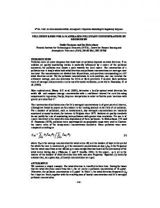
A 300 A Alo.3G%.7As stop-etch layer and a 1.0 pm thick GaAs cap ..... J. M. Mumolo, N. Q. Tran, J. D. Vincent, C. A. Shott, J. Long, and P. D. LeVan, 47, pp. 4.
UNCLASSIFIED
MULTI-BAND GaAdAlGaAs QUANTUM WELL INFRARED PHOTODETECTOR (QWIP) FOCAL PLANE ARRAYS S. V. Bandara, S. D. Gunapala, J. K. Liu, S. B. Rafol, C. A. Shott*,R. Jones*, S. Laband*, J. Woolaway II*, J. M. Fastenau**,A. K. Liu**,M. Jhabvala' , and K. K. Choi++ Jet Propulsion Laboratory, California Institute of Technology 4800 Oak Grove Drive, Pasadena, CA 91 109 *Indigo Systems Corporation, Santa Barbara, CA 93 111 ** IQE Inc., Bethlehem, PA 18015 'NASA Goddard Space Flight Center, Greenbelt, MD 2077 1 ++Army research Laboratory, Adelphi, MD 20783 ABSTRACT The GaAs/AlGaAs based Quantum Well Infrared Photodetectors (QWIPs) afford greater flexibility than the usual extrinsically doped semiconductor IR detectors because the wavelength of the peak response and cutoff can be continuously tailored over any wavelength between 6-20 pm. The spectral band width of these detectors can be tuned from narrow (MA 10 %) to wide ( M l h 50 %) allowing various applications. Also, QWIP offers multi-color infrared cameras which is capable of simultaneously acquiring images in different infrared bands. Each pixel of such array consists of vertically stacked, independently readable, QWIP detectors sensitive in different narrow infrared bands. In this article, we discuss the development and results of the 640x512 dual-band and four-band QWIP FPAs.
-
-
INTRODUCTION Long Wavelength Infrared (LWIR) staring focal plane arrays (FPAs) play critical roles in many defense applications as well as NASA's earth science, spacescience and human exploration applications. The vast majority of applications are in 6-16 micron infrared band because photons in this band can excite rotational and vibrational modes of various species of gas molecules generating absorption and emission bands in the infrared spectrum. In additional, tactical missions usually require FPAs operating in the atmospheric LWIR window (8-12 pm). Large format, staring FPAs have obvious advantages over the earlier generations of linear scanning arrays because they focus on an entire wide field of view uninterruptedly which gives them a much longer integration time. Together with the high uniformaty and
high stability, the focal plane give the sensor system much higher resolution and greater system sensitivity which translate into a better image with higher noise equivalent temperature difference (NEDT). Staring arrays also simplifies the whole sensor system by eliminating the scanning mechanism, related electronics and reducing the complexity. In recent years, quantum well infrared photodetectors (QWIPs) have shown remarkable progress in LWIR imaging with highly uniform large format FPAs [ 1-41. Fabricated entirely from large bandgap materials which are easy to grow and process, it is now possible to obtain large format highly uniform FPAs of QWIPs tuned to detect light at wavelengths from 6 to 25 pm in the GaAs/A1,Gal-, As material system [5-71. As a result of matured fabrication and processing technologies of the materials used, this breakthrough new technology has already demonstrated large format FPAs with high unifomity, high operability, high stability ( low l/f noise), and higher yield [5-91. In addition, high radiation tolerance is expected in QWIPs in contrast to narrow bandgap semiconductor detectors due to the use of larger bandgap material such as GaAdAIGaAs. These properties will enable in longer science missions with lower operating costs. Typically, QWIPs are fabricated out of eptiaxially grown 111-V alloy layers (GaAs, A1,Gal.,As and Ga,Inl.,As) on 3"GaAs wafers (now 4" and 6" wafers are available) [3-51 JPL has already demonstrated a 8-9 pm 640x486 QWIP camera with 22 pm pixel size [4]. These results show that an extension of the development to larger formats should be straightforward and relatively low risk. As a result of advance substrate removal process, QWIP large format WAS are completely immune to thermal mismatch problems between silicon CMOS readout and GaAs based QWIP array, temperature cycling
stacks, which are tailorable in different infrared bands. Each stack absorbs photons within the specified wavelength band allowing other photons to transmit through. Each detector is accessible via vertical contact pads running along the edges of the pixel or deep groove metallic gratings described below. In order to prevent shorting of the detectors, an insulating layer will be introduced in between the contacts and sidewalls of the QWIP active layers.
effects, and pixel delamination. In addition, high yield in fabrication and reproducibility of this technology will result in a lower cost for detector arrays than competing technologies.
TAILORABLE WAVELENGTH Unlike the responsivity . spectrums of intrinsic infrared detectors, the responsivity spectrums of QWIPs are much narrower and sharper due to their resonance intersubband absorption [6,7]. Recently, we have developed a technique to design a broad-band QWIP by replacing single quantum wells with small superlattice structures (several quantum wells separated by thin barriers) in the multi-quantum well structure [8]. Such a scheme creates an excited state miniband due to overlap of the excited state wavefunctions of quantum wells. Energy band calculations based on a two band model shows excited state energy levels spreading greater than 30 meV [8]. The spectral band width of these detectors can be tuned from narrow ( M l h 10 %) to wide (MA 50 %) allowing various applications. Thus, control of the processing allows us to tailor the QWIP characteristics tuned from narrow (Mlh 10 %) to wide ( M l h 50 %) in 6-20 pm spectral band allowing various applications. See Fig. 1.
-
-
DUAL-BAND OWIP FOCAL PLANE ARRAY The LWIR and VLWIR dualband QWIP device structure described in this section can be processed into interlace readable dualband FPA (i.e., odd rows for one color and the even rows for the other color) [4]. This scheme are that it provides simultaneous data acquisition and allows the use of currently available single color CMOS readout multiplexers. However, the disadvantage is that it does not provide a full fill factor for both wavelength bands. The device structure consists of a 30 period stack, of
-
-
Figure 20: Schematic diagram of a monolithically integrated, independently readable, QWIP stacks, which are tairolable in different infrared bands.
VLWIR QWIP structure and a 18 periods stack of LWIR QWIP structure separated by a heavily doped 0.5 pm thick intermediate GaAs contact layer (see Figure 3). The first stack (VLWIR) consists of 30 periods of a 500 8, AlxGal.,As barrier and a 60 8, GaAs well. Since the dark current of this device structure is dominated by the longer wavelength portion of the device structure, the VLWIR QWIP structure has been designed to have a bound-toquasibound intersubband absorption peak at 14.5 pm.The second stack (LWIR) consists of 18 periods of a 500 8, AlXGal.,As barrier and a narrow 40 8, GaAs well. This LWIR QWIP structure has been designed to have a bound-to-continuum intersubband absorption peak at 8.5 pm, because the photo current and dark current of the LWIR device structure is relatively small compared to the
WAVELENGTH a (p~)
Figure I : Spectral coverage and tailorability of GaAh based QWIPs in 4-20 p m wavelength range. Spectral bandwidth can be tuned to either broad or narrow bandwidths; i.e., bandwidths (Aka)can be tuned from I O - 50%.
GaAs based QWIP is an ideal candidate for large format long-wavelength multi-color FPAs due to its inherent properties such as narrow band response and wavelength tailorability[6-81. Fig. 2 shows a schematic diagram of a monolithically integrated, independently readable, QWIP
2
UNCLASSIFIED
both LWIR and VLWIR detectors is small, up to about VB VLWIR portion of the device structure. This whole = -0.5 V. Beyond that, it increases almost linearly with dualband QWIP structure is then sandwiched between 0.5 bias in both LWIR and VLWIR detectors reaching Rp = pm GaAs top and bottom contact layers doped with n = 5 0.3 (at VB = -2V) and 1 A/W (at VB= -3V), respectively. x l O I 7 ~ m -and ~ , was grown on a semi-insulating GaAs This behavior of responsivity versus bias is typical for substrate by MBE. A 300 A Alo.3G%.7Asstop-etch layer bound-to-continuum and bound-to-quasibound Q W P s in and a 1.0 pm thick GaAs cap layer were then grown in LWIR and VLWIR bands respectively. The peak situ on top of the device structure. GaAs wells of the LWIR and VLWIR stacks were doped with n = 6 ~ 1 0 ' ~ absorption quantum efficiencies of LWIR and VLWIR detectors operating at bias VB=2 V were 6.4% and and 2 . 5 ~ 1 0 ~' ~m -respectively. ~, All contact layers were 11.6%, respectively. Based on single element test detector doped to n = 5 ~ 1 0 ~' ~m ' The ~ . GaAs well doping density data, the LWIR detectors show background limited of the LWIR stack was intentionally increased by a factor performance (BLIP) at bias VB = -2 V and temperature T of two to compensate for the reduced number of quantum wells in the LWIR stack. It is worth noting that, the total = 72 K for a 300 K background with f/2 cold stop. The I I I I I I I l l r l (dark current + photo current) current of each stack can be vms -2v independently controlled by carefully designing the position of the upper state, well doping densities, and the number of periods in each MQW stack. All of these features were utilized to obtain approximately equal total currents from each MQW stack.
-
The simultaneously measured responsivity spectra of these vertically integrated dualband QWIPs are shown in Figure 4 . The responsivity of the LWIR detectors peaks at 8.4 pm and the peak responsivity (RJ of the detector is 509 mA/W at bias VB = -2 V. The spectral width and the cutoff wavelength of the LWIR detectors are A?Jh = 16% 8-9 p.m QWlP
-
-
14-1 5
Figure 4: Simultaneously measured responsivity spectrum of vertically integrated LWIR and VLWIR dualband QWIP detector (45 degree illumination).
QWlP
VLWIR detectors reached BLIP under the same operating conditions at 45 K operating temperature. Two different 2-D periodic grating structures were designed to independently couple the 8-9 and 14-15 pm radiation into the detector pixels of even and odd rows of the FPAs. The top 0.7 pm thick GaAs cap layer was used to fabricate the light coupling 2-D periodic grating for 8-9 pm detector pixels. The light coupling for 2-D periodic gratings of the 14-15 pm detector pixels were fabricated through the photosensitive LWIR MQW layers. This grating scheme short circuited all 8-9 pm sensitive detectors in all the odd rows of the WAS. Thus, the total thickness of 8-9 pm detector is limited by the grating layer thickness of the VLWIR detector. This 2-D periodic grating structure is fabricated on the detectors by using standard photolithography and SF6:BC13 selective dry etching. Te detailed dual band FPA fabrication process is described elsewhere [4].
n+GaAs CONTACT LAYERS
Figure 3: Conduction band energy diagram of the long-wavelength and very long-wavelength twocolor infrared detector. The long-wavelength (8-9 pm) sensitive MQ W stack utilizes the bound-tocontinuum intersubband absorption. The very longwavelength (14-15 pm) sensitive MQW stack utilizes the bound-to-quasibound intersubband absorption
and h, = 9.1 pm, respectively. The responsivity of the VLWIR detectors peaks at 14.4 pm and the peak responsivity (Rp) of the detector is 382 mA/W at bias VB = -2.0 V. The spectral width and the cutoff wavelength of the VLWIR detector are A?Jh = 10% and h ,= 15 pm, respectively. The measured absolute peak responsivity of
3
UNCLASSIFIED
demonstrate simultaneous dualband imagery at 8.5 and 14.5 pm. The camera is equipped with a 100 mm focal length f12 germanium lens designed to be transparent in the 8-15 pm wavelength range, for compatibility with the 8-9 and 14-15 pm dualband operation. Due to transmission properties of germanium, the 14-15 pm band has only 30% transmission. This poor optical transmission has clearly affected the VLWIR performance and image quality. The operability of 8-9 pm detector pixels is 99.7% and the operability of 14-15 pm detector pixels is 98%. Video images were taken at a frame rate of 30 Hz and Figure 5 shows simultaneously acquired 8-9 and 1415 micron images using this two-color ( L W R and VLWIR) imaging camera. Figure 6 shows a simultaneously acquired image of a filter pattern used to test the operating wavelengths of the two-color camera. The arrow and the semi-circle are open, and transmit all wavelengths. The diamond shape opening is covered with a 10 micron high-pass filter and the rectangle shape opening is covered with a 10 micron low-pass filter. This clearly verifies the 8-9 and 14-15 micron two-color operation of this dualband QWIP camera.
Figure 5: A Simultaneously acquired two-color image (same frame) with the 640x486 two-color QWIP camera. Image on the le@ is from 14-15 micron infrared and the image on the right is from 8-9 micron infrared.
These dualband FPAs were tested at a background temperature of 300 K, with f12 cold stop, and at 30 Hz frame rate. As expected (due to BLIP), the estimated and experimentally obtained NEAT values of the LWIR detectors do not change significantly at temperatures below 65 K. The estimated NEAT of LWIR and VLWIR detectors at 40 K are 36 and 44 mK, respectively. These estimated NEAT values based on the test detector data agree reasonably well with the experimentally obtained values. A dualband FPA hybrid was mounted onto the cold finger of a liquid helium cooled laboratory dewar, to
.
FOUR-BAND SPATIALLY SEPARATED FOCAL PLANE ARRAY One unique feature of this spatially separated four-band focal plane array is that the four infrared bands are independently readable on a single imaging array. This feature leads to a reduction in instrument size, weight, mechanical complexity, optical complexity and power requirements since no moving parts are needed. Furthermore, a single optical train can be employed, and the focal plane can operate at a single temperature. This four-band device structure was achieved by the growth of multi stack QWIP structures separated by heavily doped contact layers, on a GaAs substrate. Device parameters of each QWIP stack were designed to respond in different wavelength bands. Figure 7 shows the schematic device structure of a four color QWIP imager. A typical QWIP stack consists of a MQW structure of GaAs quantum wells separated by Al,Gal., As barriers. The actual device structure consists of a 15 period stack of 3-5 pm QWIP structure, a 25 period stack of 8.5-10 pm QWIP structure, a 25 period stack of 10-12 pm QWIP structure and a 30 period stack of 13-15.5 pm QWIP structure. Each photosensitive MQW stack was separated by a heavily doped (thickness 0.2 to 0.8 pm) intermediate GaAs contact layer (see Figure 7). Since the dark current of this device structure is dominated by the longest wavelength portion of the device structure, the VLWIR QWIP structure has been designed to have a bound-toquasibound intersubband absorption peak at 14.0 pm.
Figure 6: A simultaneously acquired image of a filter pattern. The arrow and the semi-circle are open, and transmit all wavelengths. The diamond shape opening is covered with a 10 micron highpass filter and the rectangle shape is covered with a 10 micron low-pass filter. This image clearly verifies the 8-9 and 14-15 micron twocolor operation of this QWIP camera.
4
UNCLASSIFIED
light coupling were extensively discussed in reference 5. The unwanted bottom detectors were electrically shorted at the end of each detector pixel row.
Other QWIP device structures have been designed to have a bound-to-continuum intersubband absorption process, because the photo current and dark current of these devices are relatively small compared to the VLWIR device. This whole four-band QWIP device structure was then sandwiched between 0.5 pm GaAs top and bottom ~ , was contact layers doped with n = 5 x 10” ~ m - and grown on a semi-insulating GaAs substrate by MBE.
Fourcolor QWlP Normalized Responsivity
Contact Laver 1
3
5
7
9
11
13
15
Wavelength (micron)
Figure 9: Normalized spectral response of the four-band QWIP focal plane array.
Figure 7: A schematic device layer diagram of a four color QWIP structure.
Typically, in single-band QWIP FPAs, quarter wavelength deep (h = V4nGaA,)grating grooves are used for efficient light coupling. However, in the four-band FPA, the thickness of the quarter wavelength deep grating grooves are not deep enough to short circuit the top three MQW QWIP stacks (e.g.: three top QWIP stacks on 1415.5 pm QWIP in Fig. 7). Thus, three-quarter wavelength groove depth 2-D gratings (h = 3 V 4 n ~ ~were , ) used to short the top unwanted detectors over the 10-12 and 1415.5 microns bands. This technique optimized the light coupling to each QWIP stack at corresponding bands while keeping the pixel (or mesa) height at the same level which is essential for indium bump-bonding process used for detector array and readout multiplexer hybridization. Figure 9 shows the normalized spectral responsivities of all four spectral bands of this four-band focal plane array.
Figure 8: Layer diagram of four-band QWIP device structure and the deep groove 2 - 0 periodic grating structure. Each nixel renresent a 640x128 nixel area of
Few QWIP FPAs were chosen and hybridized to a 640x512 CMOS multiplexer (ISC 9803) and biased at VB = - 1.1 V. At temperatures below 83 K, the signal to noise ratio of the 4-5 pm spectral band is limited by array nonuniformity, multiplexer readout noise, and photo current (photon flux) noise. At temperatures above 45 K, temporal noise due to the 14-15.5 pm QWIP’s higher dark current becomes the limitation. The 8-10 and 10-12 pm spectral bands have shown BLIP performance at temperatures between 45 and 83 K. The FPAs were backilluminated through the flat thinned substrate membrane
The individual pixels were defined by photolithographic processing techniques (masking, etching, chemical vapor deposition, metal deposition, etc.). Four separate detector bands were defined by a deep trench etch process and the unwanted spectral bands .were eliminated by a detector short-circuiting process. The unwanted top detectors were electrically shorted by a gold coated reflective 2-D etch gratings as shown in the Fig. 8. In addition to shorting, these gratings serve as light couplers for active QWIP stack in each detector pixel. Design and optimization of these 2-D gratings to maximize QWIP
5
UNCLASSIFIED
(thickness =: 1300 A). This initial array gave excellent images with 99.9% of the pixels working (number of dead pixels =: 250) , demonstrating the high yield of GaAs technology. The operability was defined as the percentage of pixels having noise equivalent differential temperature less than 100 mK at 300 K background and in this case operability happens to be equal to the pixel yield.
shows one frame of a video image taken with four-band 640x5 12 pixel QWIP camera.
ACKNOWLEDGEMENT
The research described here was performed by the Center for Space Microelectronics Technology, Jet Propulsion Laboratory, California Institute of Technology, and was sponsored by the National Aeronautics and Space Administration, breakthrough sensor & instrument component technology thrust area of the cross enterprise technology development program.
REFERENCES 1.
Sarath D. Gunapala, Jin S. Park, Gabby Sarusi, True-Lon. Lin, J o h n K. Liu, Paul D. Maker, Richard E. Muller, Craig A. Shott, and Ted Hoelter, IEEE Trans. Electron Devices, 44, pp. 45-50, (1997).
2.
Sarath D. Gunapala, J o h n K. Liu, Jin S. Park, Mani Sundaram, Craig A. Shott, Ted Hoelter, True-Lon Lin, S. T. Massie, Paul D. Maker, RichFd E. Muller, and Gabby Sarusi", IEEE Trans. Electron ' Devices, 44, pp. 51-57 (1997).
Figure IO: One frame of video image taken with the 4-15.5 microns cutoff four-band 640x512 pixel QWIP camera. The image is barely visible in the 14-15.5 microns spectral band due to the poor optical transmission of the antireflection layer coated germanium lens.
A 640x512 pixel four-band QWIP I T A hybrid was mounted onto a 84-pin lead-less chip carrier and installed into a laboratory dewar which is cooled by liquid helium to demonstrate a 4-band simultaneous imaging camera. The FPA was cooled to 45 K and the temperature was stabilized by regulating the pressure of gaseous helium. The other element of the camera is a 100 mm focal length AR coated germanium lens, which gives a 9.2Ox6.9" field of view. It is designed to be transparent in the 8-12 pm wavelength range. SEIRTMimage processing station was used to obtain clock signals for readout multiplexer and to perform digital data acquisition and non-uniformity corrections. The digital data acquisition resolution of the camera is lCbits, which determines the instantaneous dynamic range of the camera (i.e., 16,384), however, the dynamic range of QWIP is 85 Decibels. Video images were taken at a frame rate of 30 Hz at temperatures as high as T = 45 K, using a ROC capacitor having a charge capacity of 11x106 electrons (the maximum number of photoelectrons and dark electrons that can be counted in the time taken to read each detector pixel). Figure 10
3.
S. D. Gunapala, S. V. Bandara, J. K. Liu, W. Hong, M. Sundaram, P. D. Maker, R. E. Muller, R. Carralejo, and C. A. Shott, IEEE Trans. Elec. Devices 45, 1890 (1998).
4.
S. D. Gunapala, S. V. Bandara, A. Singh, J. K. Liu, S . B. Rafol, E. M. Luong, J. M. Mumolo, N. Q. Tran, J. D. Vincent, C. A. Shott, J. Long, and P. D. LeVan, 47, pp. 963-971, (2000).
5.
S. D. Gunapala, S. V. Bandara, J. K. Liu, E. M. Luong, S . B. Rafol, J. M. Mumolo, D. Z. Ting, J. J. Bock, M. E. Ressler, M. W. Wemer, P. D. LeVan, R. Chehayeb, C. A.
Kukkonen, M. Levy, P. LeVan, and M. A. Fauci", Sensors and Materials, 12, pp. 327-351, (2000).
6
6.
S. D. Gunapala and S. V. Bandara, Physics of Thin Films, edited by M. H. Francombe, and J. L. Vossen, Vol. 21, pp. 113-237, Academic Press, NY, (1995).
7.
S. D. Gunapala and S. V. Bandara, Quantum Well
Infrared Photodetector (QWIP) Focal Plane Arrays, Semiconductors and Semimetals, 62, 197-282, Academic Press. (1999).
8.
S. V. Bandara, S. D. Gunapala, J. K. Liu, E. M. Luong, J. M. Mumolo, W. Hong, D. K. Sengupta, and M. J. McKelvey, Appl. Phys. Lett. 72,2427 (1998).
9.
S. D. Gunapala, J. K. Liu, J. S. Park, T. L. Lin, and M. Sundaram "INFRARED RADIATION DETECTING DEVICE", US Patent No. 6,211,529.
UNCLASSIFIED