Proceedings of the 10th WSEAS International Conference on AUTOMATION & INFORMATION
Real Time Image and Data Acquisition, Processing and Communication Functions Implementation into a Mobile Sensor Node Configuration DAN POPESCU, RADU DOBRESCU, MAXIMILIAN NICOLAE, and CONSTANTIN VASILESCU Department of Control and Computers POLITEHNICA University of Bucharest Splaiul Independentei nr. 313, Bucharest 6, ROMANIA
[email protected] Abstract: Based on energy consumption, processing power, and communication efficiency, a mobile sensor network configuration for real time applications is analyzed. Based on programmable flexibility of DSP, the hardware and the software solutions for an Intelligent Mobile Node are presented. The node functions are the following: data acquisition from the sensors, measurement results interpretation, image acquisition and processing, and the communication in the network. Images are sent in network on request. The functional model, which is on demand configured type, is placed on an electric wheelchair. Key-Words: Mobile sensor network, Data acquisition, Wireless communication, Digital signal processing, Network management, Communication energy consumption, and Hardware structure research consists of a conceptual model and architecture elaboration for intelligent mobile sensor nodes based on internal processing theory by complementary data fusion, and a functional model, embedded system type, for image and data acquisition, processing, communication and remote visualization. The functional model which is a demand configured one, has high technical and economical performances.
1 Introduction A wireless sensor network (WSN) is a wireless network consisting of spatially distributed autonomous devices using sensors to cooperatively monitor physical or environmental conditions, such as temperature, sound, vibration, pressure, motion or pollutants, at different locations [2], [3]. Sensor nodes may change their location after initial deployment. Mobility can result from environmental influences such as wind or water, sensor nodes may be attached to or carried by mobile entities, and sensor nodes may possess automotive capabilities. In the recent past, wireless sensor networks (WSN) have found their way into a wide variety of applications and systems with vastly varying requirements and characteristics. As a consequence, it is becoming increasingly difficult to discuss typical requirements regarding hardware issues and software support. This is particularly problematic in a multidisciplinary research area such as wireless sensor networks, where close collaboration between users, application domain experts, hardware designers, and software developers is needed to implement efficient systems. The limited battery life of sensor nodes raises the efficient energy consumption as a key issue in wireless sensor networks. The main objective of our
ISSN: 1790-5117
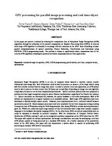
Fig.1 Mobile sensor network architecture The network is composed by moving objects
396
ISBN: 978-960-474-064-2
Proceedings of the 10th WSEAS International Conference on AUTOMATION & INFORMATION
structure of an Intelligent Mobile Node. For the Acquisition, Processing and Communication Module, each functional block is described. In Section 4 it is presented the implementation considerations for a concrete application. In this section there are explained the functions of the main loop of the software – the task launcher and of all eight tasks. It is easy to see that the concrete application is used only to demonstrate the characteristics of this approach in the conception and implementation of new equipments.
(modular nodes) with time depending topology, and therefore, with geometrical and temporal node coordinates. They are endowed with complex programmable equipments, low power consumption, able to acquire image and process data, to interact with other nodes in order to identify its position, and to communicate wireless. The system architecture can be seen in Fig.1 with the following abbreviations: NMN - network management node, IMN - intelligent mobile node, REF – reference system for tracking and localization. A sensor node (IMN) consists of two electronic modules: the first, Power and Motion Module, and the second, Acquisition, Processing and Communication Module. The streaming data coming from video interface or wireless communication interface must be processed in real-time. When new data arrives over the interface, the software must read it in before more data arrives. In this situation the software is necessary to guarantee a certain capability within a specified time constraint, so it is necessary to be in real-time. We find many Real-Time Operating Systems, shortly named RTOS, to build our application. But when the hardware designer and software designer work closely it is not difficult to develop real-time software around a task launcher and a Round Robin scheduler, without an RTOS. The idea is to divide the software into standalone, well-defined tasks and to use the task launcher as main loop. The software of IMN modules uses this solution. It is divided in eight tasks: one task which forms the communication part is for network communication and the remained seven tasks are grouped together in the application part. The main loop of the software is a task launcher included in the communication part. The link between the two parts is the objects dictionary. For a network done and for participants to communication which occupy the same hierarchical position, differences appear only at the level of the application part and at the objects dictionary. Both modules can be reprogrammed insystem to provide an application-tailored functionality [3]. The purpose of the work described in this paper is to present the acquisition, processing and communication module for an alerting system that combine the attributes of real-time operation, simplicity of realization and integration possibilities. In Section 2 there are showed some architectures for an image and data acquisition, processing and communication module. Also, it is justified the fact that DSP is the right choice for this kind of application. In Section 3 it is described the hardware
ISSN: 1790-5117
2 Acquisition, Processing Communication Module
and
When develop an acquisition, processing and communication module, depending upon their system demands, developers have a lot of architectures to choose from. ■ASIC: Designing their own chip is a route that few developers take on lightly. While ASICs give the best performance for specific applications, they are limited in their flexibility. If any design parameters are changed, the entire ASIC must be redesign. This is a process that consumes months and potentially hundreds of thousands of dollars in NRE (non-reoccurring engineering) costs. Given the complexity of designing with ASICs, the lack of adaptability to changing markets, and slow time-tomarket, ASICs are most often a less than ideal choice. ■FPGA: Field Programmable Gate Array devices provide performance close to ASICs without the delays and costs associated with re-spinning an ASIC. FPGAs, however, are as complex to design with as ASICs, and even small changes can result in the need to completely re-layout a design. FPGA devices also come with a premium price that makes them unviable in high volume applications. In certain applications, FPGA can be used to complement the DSP. ■ASSP: Application-specific standard products are ASICs that can serve a wide market. Such devices include dedicated processing engines such as MPEG-2 decoders or communications links such as USB. While these devices are low in cost because of the high market volume they typically experience, they still lack flexibility. For example, an MPEG-2 ASSP will only support a limited range of display resolutions; to introduce a new resolution requires a new ASSP and accompanying hardware redesign. ■GPP: General purpose processors offer programmability and therefore flexibility. However, many non-signal processing applications such as email, database management, and word processing
397
ISBN: 978-960-474-064-2
Proceedings of the 10th WSEAS International Conference on AUTOMATION & INFORMATION
Instruction Cycle Time, 200 MHz Clock Rate, based on the TMS320C55x DSP generation CPU processor core. The C55x™ DSP architecture achieves high performance and low power through increased parallelism and total focus on reduction in power dissipation.
don't require extensive use of multiplication. In order to keep silicon costs down for these applications, GPPs typically offer a moderately efficient multiplication instruction that takes several cycles to complete. Moreover, adding the result of each multiplication requires another instruction. As result, this makes them improper for signal processing applications. ■DSP: For implementing a real-time image and data processing applications, DSP is the best choice. DSP gives designers the best combination of power, performance, price and flexibility and allows them to quickly deliver their real-time applications to the market. Development takes place using one unified set of software tools. Because programmability is a strong suit, changes and upgrades can be quickly implemented. A multitude of integrated peripherals saves time and cost that would otherwise be spent to build the peripheral circuit. The DSP is optimized for signal processing applications compared to general purpose processors. The DSP offers many architectural features that actually reduce the number of instructions necessary for efficient signal processing. In other words, comparing performance is much more than counting instructions. The true measure is how much work is actually done. The programmable flexibility of DSP enables developers to implement complex algorithms in software. Not only can a DSP support a video codec like MPEG-2 and easily handle different resolutions with a simple software upgrade, but it can implement emerging codecs and standards as they arise without hardware redesign. Thus, having in mind the previous consideration we choose for our processing module a DSP core.
Fig.2 Structure of Intelligent Mobile Node
3 Hardware Structure The structure of the Intelligent Mobile Node is illustrated in Figure 2. It contains two functional modules: Power and Motion Module and Acquisition, Processing and Communication Module. These modules communicate each with other using the full-duplex multichannel buffered serial ports McBSP2 configured as Serial Peripheral Interface, SPI in Fig.2. The Acquisition, Processing and Communication Module contain four functional blocks. In Fig.3 it is showed the structure of Acquisition, Processing and Communication Module where we can see that this module is developed around a DSP. It is used the High-Performance, Low-Power, Fixed-Point DSP TMS320VC5509A with 5-ns
ISSN: 1790-5117
Fig.3 Block diagram of the Acquisition, Processing and Communication Module The C55x™ CPU provides two multiplyaccumulate (MAC) units, each capable of 17-bit x 17-bit multiplication in a single cycle. A central 40bit arithmetic/logic unit (ALU) is supported by an additional 16-bit ALU. The DSP peripheral set includes an external memory interface that provides access to asynchronous memories like EPROM and SRAM, as well as to high-speed, high-density memories
398
ISBN: 978-960-474-064-2
Proceedings of the 10th WSEAS International Conference on AUTOMATION & INFORMATION
inputs are supported. The TVP5150AM1 decoder includes one 9-bit analog-to-digital converter (ADC) with 2xsampling. Sampling is ITU-R BT.601 (27.0 MHz, generated from the 14.31818-MHz crystal or oscillator input) and is line locked. The output formats can be 8-bit 4:2:2 or 8-bit ITU-R BT.656 with embedded synchronization. It can see (Fig.3) that the video decoder communicates with the DSP using I2C interface and data bus. The I2C controls the decoder’s internal configuration registers while data bus is used to read digital video data through a buffer. The transfer of digital data output of video decoder is perform by the DMA of DSP. For each available data, the video decoder generates an interrupt which is synchronized with a DMA event. The DMA transfer is dependent on the occurrence of this event. Each frame taken at high speed (20 fps) is transferred in the SDRAM. DSP analyzes some rare frame (2fps) with the purpose of finding the road characteristics or ad-hoc obstacles. For improving the decision, it will be capable to access the neighbor frames of the analyzed one from the memory.
such as synchronous DRAM. Additional peripherals include Universal Serial Bus (USB), real-time clock, watchdog timer, I2C multi-master and slave interface and two channel 10-Bit successive approximation A/D. Three full-duplex multichannel buffered serial ports (McBSPs) provide the interface to a variety of industry-standard serial devices, and multichannel communication with up to 128 separately enabled channels. The DMA controller provides data movement for six independent channel contexts without CPU intervention, providing DMA throughput of up to two 16-bit words per cycle. Two general-purpose timers, seven dedicated generalpurpose I/O (GPIO) pins, and digital phase-locked loop (DPLL) clock generation are also included.
Digital block The digital block contains a DSP with the following devices: ● 32Mx16bits synchronous DRAM MT48LC32M16A2, ● 512Kx16biti Flash memory AT49BV802DT, ● Three buffered serial ports with full-duplex multichannels, which are configured as Serial Peripheral Interfaces protected by three 10-bit FET bus switches SN74CBT3384A, ● USB interface protected by low-capacitance 2channel +/-15kV ESD-protection array for highspeed data interface TPD2E001, ● Digital power supplies form the numeric block, ● JTAG interface (IEEE 1149.1) is included in this functional block.
Analogue block To enrich the analogue capabilities of Acquisition, Processing and Communication Module, an analog-to-digital converter AD7888, which contains eight single-ended analog inputs, it is used (AIN1 through AIN8 - Fig.4).
Video block The video block contains the video decoder TVP5150AM1-EP, two video cameras and the low voltage octal bidirectional buffer with 3-state inputs/outputs SN74LVT245. The TVP5150AM1 device is an ultra-low power NTSC/PAL/SECAM video decoder. Available in a space-saving 32-terminal TQFP package, the TVP5150AM1 decoder converts NTSC, PAL, and SECAM video signals to 8-bit ITU-R BT.656 format. Discrete syncs are also available. The optimized architecture of the TVP5150AM1 decoder allows for ultra-low power consumption. The decoder consumes 115mW of power in typical operation, and less than 1mW in power-down mode. Therefore, considerably increasing battery life in portable applications is allowed. The decoder uses just one crystal for all supported standards. The TVP5150AM1 decoder can be programmed using an I2C serial interface. The TVP5150AM1 decoder converts base-band analog video into digital YCbCr 4:2:2 component video. Composite and S-video
ISSN: 1790-5117
Fig.4 Analogue Block This converter is a high speed, low power, 12-bit ADC that operates from a single 2.7V to 5.25V power supply, VDD. The AD7888 is capable of a 125 kSPS throughput rate. The AD7888 features an on-chip 2.5 V reference that can be used as the reference source, VREF, for the A/D converter. The REFIN/REF OUT pin allows the user access to this reference. Alternatively, this pin can be overdriven to provide an external reference voltage for the AD7888. The voltage range for this external reference is from 1.2 V to VDD. The analog input on each of these channels is from 0 to VREF.
399
ISBN: 978-960-474-064-2
Proceedings of the 10th WSEAS International Conference on AUTOMATION & INFORMATION
of the dictionary of objects is in accord with Manufacturing Message Specification, ISO/IEC9506. These objects correspond of the measurement results of those eight analog inputs, of the captured images by those two cameras connected to video inputs of Acquisition, Processing and Communication Module and so on. The type of measurement results is integer or float and the type of captured images it is an array of octet-string, where the octet-string are dates from each video line. The task number 0 and the tasks number 2 to 7 are for application, form the application part of software structure, assuring the functionality of Acquisition, Processing and Communication Module. The communication part contains the task of communication (task_1) in network and a real time kernel. The application part contains seven tasks witch solve all the equipment demands less those in connection with the communication in network. The task number 0, task_0, process results of A/D conversions and calculate averages for sixty samples. All eight analog inputs are measured one time per second. After all eight analog inputs are measured it is prepared the launch in execution of task number 4, task_4, setting the bit flgx_4 (the status bit of task_4). Those eight analog inputs of Acquisition, Processing and Communication Module are used to measure two temperature sensors and six gas sensors. Task_2 manage the video interface. It is responsible to prepare the response a one image demand. Task_3 supervises the process. This task is responsible for all decisions in the control and the monitoring of application. The task schedule prepares the launch in execution of this task to base time. Task_4 ensures the physical unit conversion of the results obtained in task_0. Task_5 resolves the USB interface and the task_6 solves the communication with the Power and Motion Module (SPI2 interface). Task_7 keeps the history of events. We placed the Intelligent Mobile Node on an electric wheelchair (Fig.5). A CCD camera and two sonar sensors are placed in the bottom of the mechanical structure covering the space explored by a priority window, at 200 mm from the road level. The image processing algorithms implemented on IMN are the following: primary image processing [4] (local noise rejection, local edge
CMOS construction ensures low power dissipation of typically 2 mW for normal operation and 3 µW in power-down mode. It is used a 2.5V external reference with AD780. This ultrahigh precision band gap reference AD780 provides a pin programmable 2.5V or 3.oV output. Low initial error and temperature drift combined with low output noise and the ability to drive any value of capacitance make the AD780 the ideal choice for enhancing the performance of ADC. The 12-bit ADC AD7888 communicates with the DSP using the full-duplex multi-channel buffered serial ports McBSP1 configured as Serial Peripheral Interface (SPI1). Communication block The communication block uses the MC13202 transceiver. This is a short range, low power, 2.4 GHz Industrial, Scientific, and Medical (ISM) band transceivers. The MC13202 contains a complete 802.15.4 physical layer (PHY) modem designed for the IEEE® 802.15.4 Standard which supports peerto-peer, star, and mesh networking. The transceiver includes a low noise amplifier, 1.0mW power amplifiers (PA), onboard RF transmit/receive (T/R) switch for single port use, PLL with internal voltage controlled oscillator (VCO), on-board power supply regulation, and full spread-spectrum encoding and decoding. The device supports 250 kbps Offset-Quadrature Phase Shift Keying (O-QPSK) data in 2.0 MHz channels with 5.0 MHz channel spacing per the 802.15.4 Standard. The MC13202 transceiver communicates with the DSP using the full-duplex multi-channel buffered serial ports McBSP0 configured as Serial Peripheral Interface, SPI0 in Fig.3.
4 Implementation Considerations The Mobile Sensor Network can be used into alerting system. In this system each Intelligent Mobile Node – IMN, is connected up to eight sensors and up two video cameras. The IMN trough the Acquisition, Processing and Communication Module measure the sensors, interpret the measurement results, capture images, processing and communicate in network. Images are sent in network to demand. For this system it is necessary to be developed software for each structure of system. The software of Acquisition, Processing and Communication Module is divided in a communication part and an application part. The link between the communication and application part is the dictionary of objects. The type of objects
ISSN: 1790-5117
400
ISBN: 978-960-474-064-2
Proceedings of the 10th WSEAS International Conference on AUTOMATION & INFORMATION
Local Processors for On-Line Processing with Applications in Intelligent Vehicle Technologies, Proceedings of the 10th WSEAS International Conference on SYSTEMSAthens, Greece, July 10-12, 2006, pp 579-584; [5] R.Dobrescu, D.Popescu, and M.Nicolae: Mobile Node Implementation for WSN Applications, International Journal Of Circuits, Systems And Signal Processing, Issue 1, Vol.2, 2008, pp 121-130; [6] D.Popescu, R.Dobrescu, D.Merezeanu: Road Analysis Based on Texture Similarity Evaluation, Proceedings of the 7th WSEAS International Conference on SIGNAL PROCESSING (SIP’08), Istambul, Turkey, May 27-30, 2008, pp.47-51; [7] *** TMS320VC5509A Fixed-Point Digital Signal Processor Data Manual, Texas Instruments Inc., November 2002 − Revised January 2008; [8] ***TMS320C55x DSP Peripherals Overview Reference Guide, Texas Instruments Inc., April 2006; [9] ***AD7888 2.7 V to 5.25 V, Micropower, 8Channel,125 kSPS, 12-Bit ADC in 16-Lead TSSOP, Analog Devices Inc, Rev. B 2001; [10] D.J.Pack and S. F. Barrett, 68HC12 Microcontroller Theory and Applications, Prentice-Hall Inc., 2002, Upper Saddle River, NJ [11] J. Beveridge, and R. Wiener, Multithreading Application in Win32, Addison Wesley Longman, Inc., 1997. [12] L.M. Bazinet, et. al. QNX 4 Operating System – System Architecture, QNX Software Systems Ltd,, 1995; [13] H. Karl and A. Willig, Protocols and Architectures for Wireless Sensor Networks, Wiley, 2007; [14] S. Olariu, L. Wilson, M. Eltoweissy and K. Jones, Training a wireless sensor network, Mobile Networks and Applications, 10, 2005, pp. 151-167; [15] F. Akyildiz, W. Su, Y. Sankarasubramanian, and E. Cayirci, Wireless sensor networks: A survey, Computer Networks, 38 (4), 2002, pp. 393–422; [16] D. Estrin, R. Govindan, J. Heidemann and S. Kumar, Next century challenges: Scalable coordination in sensor networks, MobiCom, 1999, pp. 263-270; [17] W. Ye, J. Heidemann, and D. Estrin, An Energy-Efficient MAC protocol for Wireless Sensor Networks, INFOCOM, pp. 1567-1576, June 2002.
extraction, segmentation), texture analysis, and minimum distance – based image classification [6].
Fig.5. Experimental platform for the Intelligent Mobile Node testing. Only the results of these local image processing operations are regulary transmited to management node. The whole image frames are transmited by request to the management node.
5 Conclusion The method based on the divide the software in a communication part and an application part, developed around a task launcher and a Round Robin scheduler allow the achievement of new equipments what operate in real-time, for image and data acquisition, processing and communication. For the purpose of energy saving, a careful analysis of local and central processing resources must be made. Also, the balance between local communication energy consumption and local processing energy consumption must be taken into account.
References: [1] K. Römer, M. Friedemann, The Design Space of Wireless Sensor Networks, IEEE Wireless Communications 11 (6), p.54–61, 2004. [2] T.Haenselmann, An FDL'ed Textbook on Sensor Network, Published under the GNU Free Documentation License, 2006. [3] R. Dobrescu, D. Popescu, M. Nicolae, Design of a Modular Node for Tracking, Localization and Data Acquisition for WSN Applications, Proceedings 4th WSEAS International Conference on REMOTE SENSING (REMOTE’08) – Venice, Italy, November 2123, 2008, p.51-56. [4] D.Popescu, R.Dobrescu, V.Avram, St.Mocanu,
ISSN: 1790-5117
401
ISBN: 978-960-474-064-2