... first trap in HfO2. The memristive properties of ALD grown TiN/HfO2/TiN devices are correlated with the demon- ... ces has attracted renewed attention as a functional basis for .... the curve slope is larger than that in SCLC (s$2).20. The best ...
[This article is copyrighted as indicated in the article. Reuse of AIP content is subject to the terms at: http://scitation.aip.org/termsconditions. Downloaded to ] IP: 93.175.19.129 On: Mon, 26 Jan 2015 15:25:43
JOURNAL OF APPLIED PHYSICS 117, 044901 (2015)
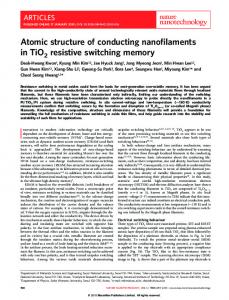
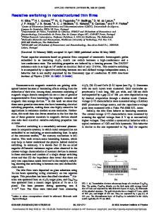
Resistive switching and synaptic properties of fully atomic layer deposition grown TiN/HfO2/TiN devices Yu. Matveyev,1,2 K. Egorov,1 A. Markeev,1 and A. Zenkevich1,2 1
Moscow Institute of Physics and Technology, 141700 Moscow Region, Russia NRNU “Moscow Engineering Physics Institute”, 115409 Moscow, Russia
2
(Received 8 October 2014; accepted 30 December 2014; published online 26 January 2015) Recently proposed novel neural network hardware designs imply the use of memristors as electronic synapses in 3D cross-bar architecture. Atomic layer deposition (ALD) is the most feasible technique to fabricate such arrays. In this work, we present the results of the detailed investigation of the gradual resistive switching (memristive) effect in nanometer thick fully ALD grown TiN/HfO2/TiN stacks. The modelling of the I-V curves confirms interface limited trap-assisted-tunneling mechanism along the oxygen vacancies in HfO2 in all conduction states. The resistivity of the stack is found to critically depend upon the distance from the interface to the first trap in HfO2. The memristive properties of ALD grown TiN/HfO2/TiN devices are correlated with the demonstrated neuromorphic functionalities, such as long-term potentiation/depression and spike-timing dependent plasticity, thus indicating their potential as electronic synapses in neuromorphic hardC 2015 AIP Publishing LLC. [http://dx.doi.org/10.1063/1.4905792] ware. V I. INTRODUCTION
While the modern computing paradigm based on the complementary metal-oxide-semiconductor (CMOS) logic and the classical von Neumann digital architecture is optimal for processing well-defined data sets, it cannot compete with their biological counterparts in solving the problems of the real world, such as image and voice recognition, navigation, etc. Even though digital computers can reach the speed and complexity to emulate the functionality of some animals, the energy dissipation in the system grows exponentially with the increasing hierarchy of animal intelligence. The reason is that the biological brain is configured differently, and the key features are extremely high (!104) connectivity between neurons in a very compact three-dimensional network which offers highly parallel processing power, extremely high power efficiency, the combination of storage and computation, and self-learning and adaptivity ✓ to changing environments.1 For years, the implementation of the artificial neural networks has been in the form of software run on conventional “von Neumann” computers, but such simulations appear incomparable to the biological systems in terms of speed and energy efficiency. Even the neural networks based on the purpose-built integrated circuits are far inadequate using the current technology. Generally, a fundamental drawback of the software solutions to artificial intelligence lies in the need to transfer the data between a memory, which stores the software data, and a processor, which computes based on the data. This requirement of data transfer generates an intrinsic delay and inefficiency, which limits all CMOS-based neural networks. Therefore, the challenge is to build brain-inspired, “neuromorphic” computational systems, which mimic the ability of the brain to perform energy-efficient and fault-tolerant computation, as well as to combine memory and computation in single elements. However, until recently, the building of such three0021-8979/2015/117(4)/044901/7/$30.00
dimensional compact artificial hardware neural networks providing the complexity, connectivity, and massive parallel information processing remained elusive, particularly due to the lack of a compact element emulating the functionality of the biological synapse. Meanwhile, over the last decade, broad set of reversible electrical resistance-switching phenomena in thin-film devices has attracted renewed attention as a functional basis for the alternative nonvolatile memory technologies.1 Among different approaches, a particularly promising concept is a memristor (memory þ resistor)—a simple nanoscale two terminal thin-film device exhibiting multi-level resistance switching.2 Moreover, the gradual, analog-like transition between the resistance states observed in memristors under carefully optimized conditions appears to emulate the plasticity of biological synapses, and it has been shown previously that devices based on different material systems effectively mimic such properties as long term potentiation and depression,3,4 pair-pulse fluctuation,5 and spike-timing dependent plasticity (STDP).3,4,6,7 Other properties of memristors, such as the demonstrated scaling to nm size, low energy consumption per switching event and the possibility for three-dimensional (3D) integration in crossbar geometries, make them attractive candidates for synaptic devices. Indeed, several works demonstrating the experimental implementation of simple memristive neural networks have been already published [e.g., Refs. 8 and 9]. In addition, it has been argued that crossbar memristor arrays can be successfully integrated with the current CMOS technology.10 Such hybrid memristor/CMOS systems are appealing since they offer the potential to develop a new paradigm for “neuromorphic computing” modelling the biologic brain. Among a variety of fabrication methods to produce thinfilm structures exhibiting resistive switching behavior, Atomic Layer Deposition (ALD) is one of the feasible techniques, since it is already integrated with the modern
117, 044901-1
C 2015 AIP Publishing LLC V
[This article is copyrighted as indicated in the article. Reuse of AIP content is subject to the terms at: http://scitation.aip.org/termsconditions. Downloaded to ] IP: 93.175.19.129 On: Mon, 26 Jan 2015 15:25:43
044901-2
Matveyev et al.
microelectronic technology and provides both atomic-level control in thickness and conformality on complicated 3D surface topologies.11 In this work, we present the results of the detailed investigation of the resistive switching mechanism in HfO2 based stacks with TiN electrodes, fully grown by ALD on Si substrates. HfO2/TiN system has been extensively studied in the context of the resistive switching previously [e.g., Refs. 12–16]. Despite the general agreement that the resistivity in HfOx is defined by the conducting filaments associated with the oxygen vacancies, several essentially different mechanisms have been proposed. In particular, trap-assisted tunneling including the critical role of the gap distance between the interface and the first trap was revealed in TiN/HfO2/Pt memory stacks,13,16 while a semiconductinglike nature of oxygen-deficient filaments in HfOx requiring the formation of !10% concentration of oxygen vacancies was alternatively claimed to describe the conductivity in the low resistance state.14 In this work, basing on the systematic (temperature dependent) electrical measurements in different conduction states of ALD grown TiN/HfO2/ TiN memory stacks, we conclude about the interface limited trap-assisted tunneling mechanism of conductivity in HfOx irrespective of the resistance state of the device. We further exploit the revealed memristive properties of our TiN/HfO2/TiN devices to demonstrate their synaptic functionalities. II. EXPERIMENTAL DETAILS
TiN/HfO2/TiN stacks were grown in a single vacuum cycle by ALD using a vertical type Sunale R-100 Picosun OY ALD reactor. Si(100) wafers with native oxide were used as a substrate. TiN layers were deposited at the substrate temperature T ¼ 420 $ C using TiCl4 and NH3 precursors, while HfO2 layers were grown at T ¼ 240 $ C using Hf[N(CH3)(C2H5)]4 and H2O as precursors of Hf and O, respectively. Both bottom and top TiN electrodes were !20 nm thick, while HfO2 layer chosen for this study is 6 nm in thickness. According to the transmission electron microscopy analysis of the stack cross-section (not shown), HfO2 layer is polycrystalline. It is important to note that due to peculiarities of the growth and patterning procedures an ultrathin (!0.5–1 nm) partially oxidized TiOxN1%x layer is present at the bottom interface, in contrast with the sharp top interface. The detailed chemical analysis of constituents across the stack by in vacuo x-ray photoelectron spectroscopy is reported elsewhere17 and the growth rate was calibrated by ellipsometry. In order to prepare top electrodes, the upper TiN layer was patterned using standard optical lithography procedures, thus defining circular pads 50 lm in diameter. The electrical measurements were performed at room temperature using Cascade Summit 1100 probe station coupled with Agilent semiconductor device analyzer B1500A containing two B1530A pulse generators and two source measurement units connected via a selector. During DC I-V and pulse train tests, the bias was applied to the top TiN electrode with the bottom TiN electrode grounded. To perform STDP tests, the top and bottom electrodes in the
J. Appl. Phys. 117, 044901 (2015)
TiN/HfO2/TiN device were connected to separate pulse generators. III. RESULTS AND DISCUSSION
The results of DC I-V measurements are shown in Fig. 1. As grown structures require electrical forming by positive bias sweep up to U ¼ 4 V with the current compliance (CC) at 1 mA. During the electroforming, the resistance drops from R ! 109 X down to R ! 103 X (here and further the resistance is given at the bias U ¼ 0.1 V). Lower CC level during the forming process does not result in the higher resistance or smaller operation current, but rather leads to the decrease of yield in the number of working devices. During the following first reset cycle with the voltage sweep down to U ¼ %1.7 V without CC, the resistance instead increases from R ! 103 X up to !105 X. Following this procedure, the TiN/HfO2/TiN devices exhibit reversible resistive switching effect in DC I-V regime with the “SET” (RESET) voltage USET ! 1.1 & 1.3 (URESET ! %1.5 & %1.7 V) (Fig. 1). Except from the small initial step at U ! 0.75 V, the SET transition in our devices is gradual, and we thus do not need to use any CC. The ratio RLRS/RHRS can be adjusted by varying USET and URESET within the full range of R ! 10 kX & 200 kX. It is worth to notice that in the regular switching regime the device resistance never drops down to R ! 103 X (the value after the forming step). The apparent reason for this is the “overshooting” current during the forming process due to an unavoidable delay of CC circuit (!10%5 s for our measuring device). For further investigation, we select the range between RLRS ! 15 kX and RHRS ! 150 kX. If the resistive switching is triggered by the trapezoidal pulses s ¼ 1:5 ls; with 0:5 ls edges, the operation voltage increases to the levels USET ! 1.5 & 1.8 V and URESET ! %2 & %2.3 V. The endurance of the devices in one-pulse switching mode is estimated to be >104 cycles, taking the decrease of RLRS/RHRS ratio to the values 104 with ROff/ROn ' 10. The detailed analysis of current-voltage curves suggests that the devices exhibit interface limited trap-assisted tunneling conductivity mechanism in all resistance states. Based on this analysis, we reveal that the resistance across HfO2 layer depends on the oxygen vacancy distribution and is limited by the tunneling distance to the first trap, which is defined by the TiON interfacial layer. We have shown that TiN/HfO2/TiN devices can integrate pulses of current and thus exhibit long term potentiation and depression properties similar to that of biological synapses. By using a pair of equivalent time-delayed electrical pulses with the shape that mimic spikes in real neurons, we have further emulated spike-timing dependent plasticity function in such fully ALD grown devices. We therefore conclude that TiN/HfO2/TiN devices are promising candidates for hardware implementation of hybrid CMOS-neuron/ memristor-synapse bio-inspired neuromorphic systems. ACKNOWLEDGMENTS
The work was supported by the Russian Science Foundation Grant No. 14-19-01698. 1
D. Kuzum, S. Yu, and H.-S. P. Wong, Nanotechnology 24, 382001 (2013). D. B. Strukov, G. S. Snider, D. R. Stewart, and R. S. Williams, Nature 453, 80–83 (2008). 3 K.-H. Kim, S. Gaba, D. Wheeler, J. M. Cruz-Albrecht, T. Hussain, N. Srinivasa, and W. Lu, Nano Lett. 12, 389–395 (2012). 4 S. Yu, B. Gao, Z. Fang, H. Yu, J. Kang, and H.-S. P. Wong, Adv. Mater. 25, 1774–1779 (2013). 5 S. G. Hu, Y. Liu, T. P. Chen, Z. Liu, Q. Yu, L. J. Deng, Y. Yin, and S. Hosaka, Appl. Phys. Lett. 102, 183510 (2013). 6 Y. Li, Y. Zhong, J. Zhang, L. Xu, Q. Wang, H. Sun, H. Tong, X. Cheng, and X. Miao, Sci. Rep. 4, 4906 (2014). 7 S. Mandal, A. El-Amin, K. Alexander, B. Rajendran, and R. Jha, Sci. Rep. 4, 5333 (2014). 8 F. Alibart, E. Zamanidoost, and D. B. Strukov, Nat. Commun. 4, 2072 (2013). 9 M. Ziegler, R. Soni, T. Patelczyk, M. Ignatov, T. Bartsch, P. Meuffels, and H. Kohlstedt, Adv. Funct. Mater. 22, 2744–2749 (2012). 10 J. Borghetti, Z. Li, J. Straznicky, X. Li, D. A. A. Ohlberg, W. Wu, D. R. Stewart, and R. S. Williams, Proc. Natl. Acad. Sci. U.S.A. 106, 1699–1703 (2009). 11 J. Y. Seok, S. J. Song, J. Y. Yoon, K. J. Yoon, T. H. Park, D. E. Kwon, H. Lim, G. H. Kim, D. S. Jeong, and C. S. Hwang, Adv. Funct. Mater. 24, 5316–5339 (2014). 12 S. Yu, Y. Wu, D. Kuzum, and H.-S. P. Wong, IEEE Trans. Electron. Devices 58, 2729 (2011). 13 S. Yu, X. Guan, and H.-S. P. Wong, Appl. Phys. Lett. 99, 063507 (2011). 14 F. De Stefano, M. Houssa, J. A. Kittl, M. Jurczak, V. V. Afanas’ev, and A. Stesmans, Appl. Phys. Lett. 100, 142102 (2012). 15 S. Cimino, A. Padovani, L. Larcher, V. V. Afanas’ev, H. J. Hwang, Y. G. Lee, M. Jurczac, D. Wouters, B. H. Lee, H. Hwang, and L. Pantisano, Microelectr. Eng. 95, 71–73 (2012). 16 L. Zhao, H.-Y. Chen, S.-C. Wu, Z. Jiang, S. Yu, T.-H. Hou, H.-S. Philip Wong, and Y. Nishi, Nanoscale 6, 5698 (2014). 17 K. V. Egorov, R. V. Kirtaev, Yu. Yu. Lebedinskii, A. M. Markeev, Yu. A. Matveyev, O. M. Orlov, A. V. Zablotskiy, and A. V. Zenkevich, “Complementary and bipolar regimes of resistive switching in TiN/HfO2/ 2
[This article is copyrighted as indicated in the article. Reuse of AIP content is subject to the terms at: http://scitation.aip.org/termsconditions. Downloaded to ] IP: 93.175.19.129 On: Mon, 26 Jan 2015 15:25:43
044901-7
Matveyev et al.
TiN stacks grown by atomic-layer deposition,” Status Solidi A (published online). 18 T. Cabout, L. Perniola, V. Jousseaume, H. Grampeix, J. F. Nodin, A. Toffoli, M. Guillermet, E. Jalaguier, E. Vianello, G. Molas, G. Reimbold, B. De Salvo, T. Diokh, P. Candelier, O. Pirrotta, A. Padovani, L. Larcher, M. Bocquet, and C. Muller, in Proceedings of the IEEE 5th International Memory Workshop (2014), pp. 116–119. 19 M. A. Lampert, Phys. Rev. 103, 1648 (1956). 20 J. F. Scott, C. A. Araujo, B. M. Melnick, L. D. McMillan, and R. Zuleeg, J. Appl. Phys. 70, 382–388 (1991). 21 T. Mihara and H. Watanabe, Jpn. J. Appl. Phys., Part 1 34, 5664–5673 (1995). 22 D. S. Jeong and C. S. Hwang, J. Appl. Phys. 98, 113701 (2005).
J. Appl. Phys. 117, 044901 (2015) 23
C. Walczyk, C. Wenger, R. Sohal, M. Lukosius, A. Fox, J. Da˛browski, D. Wolansky, B. Tillack, H.-J. M€ ussig, and T. Schroeder, J. Appl. Phys. 105, 114103 (2009). 24 K. Xiong, J. Robertson, M. C. Gibson, and S. J. Clark, Appl. Phys. Lett. 87, 183505 (2005). 25 Yu. A. Matveyev, A. M. Markeev, Yu. Yu. Lebedinskii, A. A. Chouprik, K. V. Egorov, W. Drube, and A. V. Zenkevich, Thin Solid Films 563, 20–23 (2014). 26 T. Serrano-Gotarredona, T. Masquelier, T. Prodromakis, G. Indiveri, and B. Linares-Barranco, Front. Neurosci. 7, 2.1–2.15 (2013). 27 S. F. Cooke and T. V. P. Bliss, Brain 129, 1659–1673 (2006). 28 G.-Q. Bi and M.-M. Poo, J. Neurosci. 18, 10464–10472 (1998). 29 R. Q. Quiroga, J. Neurosci. Methods 177, 194–198 (2009).
[This article is copyrighted as indicated in the article. Reuse of AIP content is subject to the terms at: http://scitation.aip.org/termsconditions. Downloaded to ] IP: 93.175.19.129 On: Mon, 26 Jan 2015 15:25:43