Power-Efficient Computation Based on Difference Schemes. Kentaro Sanoâ ... governing equations of physics, which are approximated by ap- plying the ...
Scalable FPGA-Array for High-Performance and Power-Efficient Computation Based on Difference Schemes Kentaro Sano† WANG Luzhou Yoshiaki Hatsuda Satoru Yamamoto Graduate School of Information Sciences,Tohoku University 6-6-01 Aramaki Aza Aoba, Aoba-ku, Sendai 980-8579, JAPAN Email: {kentah, limgys, hatsuda, yamamoto}@caero.mech.tohoku.ac.jp Abstract— For numerical computations requiring a relatively high ratio of data access to operation, the scalability of memory bandwidth is key to performance improvement. In this paper, we propose a scalable FPGAarray to achieve custom computing machines for high-performance and power-efficient scientific simulations based on difference schemes. With the FPGA-array, we construct a systolic computational-memory array (SCMA) by homogeneously partitioning the SCMA among multiple tightly-coupled FPGAs. A large SCMA implemented using a lot of FPGAs achieves highperformance computation with scalable memory-bandwidth and scalable arithmetic-performance according to the array size. For feasibility demonstration and quantitative evaluation, we design and implement the SCMA of 192 processing elements over two ALTERA StratixII FPGAs. The implemented SCMA running at 106MHz achieves the sustained performances of 32.8 to 36.5 GFlops in single precision for three benchmark computations while the peak performance is 40.7 GFlops. In comparison with a 3.4GHz Pentium4 processor, the SCMAs consume 70% to 87% power and require only 3% to 7% energy consumption for the same computations. Based on the requirement model for inter-FPGA bandwidth, we illustrate that SCMAs are completely scalable for the currently available high-end to low-end FPGAs, while the SCMA implemented with the two FPGAs demonstrates the doubled performance of that by the single-FPGA SCMA.
I. I NTRODUCTION Scientific simulation based on finite difference methods is one of the major applications requiring high-performance computing (HPC) with floating-point operations, which includes thermal propagation problems, fluid dynamics problems, electromagnetic problems and so on. These simulations numerically solve the partial differential equations (PDEs) constructing the governing equations of physics, which are approximated by applying the difference schemes with discrete values defined at 2D or 3D grid points. Since computation of each grid-point requires data of its multiple neighbors, such simulations are memoryintensive applications. Therefore, not only the peak arithmetic performance but also scalable memory-bandwidth is necessary for the high-performance scientific simulation. However, the general-purpose computers commonly used for HPC are based on an inefficient structure in terms of bandwidth. A microprocessor has the memory-bandwidth problem, which is so-called the von Neumann bottleneck. While the amount of hardware resources available on a chip has been steadily growing with technology scaling, the bandwidth through the chip I/O pins has been narrowly improved with difficulty. Thus, even though a cache memory is effective, the off-chip main memory is very far from the processor, and its bandwidth is inherently insufficient for memory-intensive applications. Under these circumstances, custom computing machines (CCMs) are expected to achieve efficient and scalable computa† Corresponding author. c 978-1-4244-2826-7/08/ $25.00 �2008 IEEE
tion with customized data-paths, memory systems and a network for each individual application. Especially, field-programmable gate arrays (FPGAs) are nowadays becoming very attractive devices to implement CCMs for HPC. Thanks to the remarkably advanced FPGA technology, more and faster resources, e.g., logic elements (LEs), DSP blocks, embedded memories and I/O blocks, have been integrated on an FPGA with less power consumption. Consequently, the potential performance of FPGAs now overcomes that of general-purpose microprocessors for floating-point computations [1, 2]. Accordingly, a lot of researchers have been trying to exploit FPGAs for floating-point applications for years [3–10]. In our previous work [11], we proposed the systolic computational memory (SCM) architecture for scalable simulation of computational fluid dynamics (CFD), and demonstrated that the single-FPGA implementation of a systolic computationalmemory array (SCMA) achieves higher performance and higher efficiency than those of a general-purpose microprocessor. The decentralized memories coupled with local processing elements (PEs) of the SCM architecture theoretically provide complete scalability of both entire memory-bandwidth and arithmetic performance by increasing the array size. However, the feasibility of this scalability is not sufficiently verified for multipleFPGA implementation, which is indispensable to a larger array for much higher performance. This paper proposes a scalable FPGA-array allowing a generalized SCMA to be extensible over multiple FPGAs for powerefficient HPC of the scientific simulations based on the difference schemes. First, we provide our design concept of the generalized SCMAs as reconfigurable CCMs composed of the configurable hardware part and the software part, which give a static but customized structure and dynamic flexibility, respectively, for wider target applications. Based on this concept, we describe our design of the SCMA for not only CFD, but also computations based on difference schemes. Second, we introduce homogeneous partitioning of an SCMA into sub-arrays for scalable multiple-FPGA implementation. We map the sub-arrays onto tightly-coupled FPGAs connected with a 2D mesh network. Since the inter-FPGA bandwidth can limit the performance of each FPGA in employing multiple FPGAs, we formulate the bandwidth requirement model with the communication frequency in a computational program. Through implementation with two FPGAs, we demonstrate that the two FPGAs achieve the doubled performance of that by a single FPGA. We show that these FPGAs also have the advantage of low power-consumption in comparison with an actual micropro-
cessor. Moreover, based on the bandwidth requirement model, we project that SCMAs are completely scalable with currently available high-end to low-end FPGAs. This paper is organized as follows. Section II summarizes related work. Section III describes the target computations, the architecture and design of an SCMA, and the performance constraint model concerning the inter-FPGA bandwidth. Section IV explains the SCMA implementation using two ALTERA Stratix II FPGAs, evaluates its performance and power/energy consumption for three benchmark computations, and discusses the scalability of SCMAs with commercially available FPGAs. Finally, Section V gives conclusions and future work. II. R ELATED W ORK As FPGAs have been getting more and faster components of LEs, DSPs and embedded RAMs, their potential performance for floating-point operations has increased rapidly. There have been many reports about floating-point computations with FPGAs: fundamental researches of floating-point units on FPGAs [3], linear algebra kernels [4–6, 12, 13] and performance analysis or projections [1, 2]. FPGA-based acceleration of individual floating-point application has been presented for iterative solvers [14], FFT [15], adaptive beamforming in sensor array systems [16], seismic migration [8], transient waves [9], molecular dynamics [10, 17, 18] and finance problems [19, 20]. There has been work attempting to use FPGAs for acceleration of numerical simulations based on finite difference methods: the initial effort to build an FPGA-based flow solver [21], the overview toward an FPGA-based accelerator for CFD applications [22], the proposals for FPGA-based acceleration of finite-difference time-domain (FDTD) method [7, 23, 24]. However, they are not such scalable and inclusive acceleration of these numerical simulations that we are aiming at. In contrast to the above previous work, the approach proposed in this paper is based on the discussion of architectures suitable for scalability of both arithmetic performance and memory-bandwidth. We design our FPGA-based CCMs so that they can handle a group of computations based on difference schemes, instead of only a single specific computation. III. S CALABLE FPGA-A RRAY A. Target computation The target computation of our FPGA-based CCMs is the numerical simulation based on finite difference methods, which is one of the major application groups requiring high-performance floating-point computations. The simulation numerically solves the governing equations that are the partial differential equations (PDEs) modeling the physics. The PDEs are numerically approximated by applying the difference schemes with discrete values defined at 2D or 3D grid points for discrete time-steps. Let’s assume that we have a 2D function q(x, y) in PDEs, which is expressed with discrete values qi, j at grid-points (i, j). The central-difference schemes of the 2nd-order accuracy give the following approximations. qi+1, j − qi−1, j ∂q � , ∂x 2Δx
qi−1, j − 2qi, j + qi+1, j ∂ 2q � 2 ∂x Δx2
(1)
where Δx is the interval of adjacent grid-points in the x direction. With these approximations, the PDEs are expressed in the following common form [11]: qnew i, j = c0 + c1 qi, j + c2 qi+1, j + c3 qi−1, j + c4 qi, j+1 + c5 qi, j−1 (2) where c0 to c5 are constants or values obtained only with values at (i, j). We refer to this computation as neighboring accumulation. In the case of the 3D grid, the accumulation contains at most eight terms. Thus, the difference schemes allow the numerical simulations to be performed by computing the neighboring accumulations. We can also compute higher-order difference schemes with a combination of the neighboring accumulations. Eq.(2) means that all grid-points just require the accumulation computations only with data of the adjacent ones. The computations at all grid-points are independent, so that they can be performed in parallel. To exploit these properties of the locality and the parallelism, an array of processing elements (PEs) performing parallel computation with decomposed subdomains is suitable [25]. Moreover, due to the computational homogeneity among grid-points, computations based on the difference schemes are described as a systolic algorithm, which can efficiently be performed by a systolic array [26, 27] in parallel. B. Architecture While recent advancement in semiconductor technology provides VLIs abundant in transistors with slightly increased I/O pins, performance improvement is not limited by computation itself, but the memory bandwidth, i.e., the von Neumann bottleneck. Reconfigurable computing with FPGAs is a promising approach to achieve scalable memory-bandwidth by builting custom computing machines (CCMs) tailored for target problems, instead of the conventional computing-prioritized processors. Then, what architecture is suitable to design CCMs with scalable memory-bandwidth for HPC? Our answer to this question is the systolic computational-memory (SCM) architecture, which is the combination of the systolic architecture (or other 2D array architectures [25]) and the computational memory approach. The systolic array [26, 27] is a regular arrangement of many processing elements (PEs) in an array, where data are processed and synchronously flow across the array between neighbors. Since such an array is suitable for pipelining and spatially parallel processing with input data while they pass through the array, it gives scalable arithmetic performance according to the array size. In addition to this scalable arithmetic performance, the computational-memory approach provides scalable memory-bandwidth. This approach is similar to computational RAM (C*RAM) or “processing in memory” concept [28–31], where computing logic and memory are arranged very close to each other. In our SCM architecture, the entire array behaves as the memory not only storing data but also performing floatingpoint operations with them by itself. The memory is partitioned into local memories decentralized to PEs, which concurrently perform computation with the data stored in their local memories. This structure allows the internal-memory bandwidth of the array to be wide and scalable to its size.
FPGA0 Logic Mem
FPGA2 Logic Mem
Logic Mem
Microoperation Sequence: MS
Logic
Memory Read: MR
Mem
32
PE Logic Mem
Logic Mem
Logic Mem
Logic Mem
Logic Mem
Logic Mem
Logic Mem
Logic Mem
Switch
8
Comp units Local Memory
aSrc
write data
32
read data 1
0
Sequencer 8
microoperation
M u x
32
M u 0x
32
32
write addr
1
Local Memory 8
Execute1: EX2 EX3 EX4 EX5 Write EX1 Back:WB
32 1
readAddr1
32
in-a
32
read data 2
in-b
out
Floating-Point MAC: ab (5 stages)
sign
readAddr2
bSrc
accSelect
8
wAddr vSrc
Logic Mem FPGA1
Logic Mem
Logic Mem
Logic Mem
Controller for PEs
hSrc
32
N-FIFO out 32
S-FIFO out
32 1
M u 0x
E-FIFO out
1
32
W-FIFO out
0
M u x
in N-FIFO’
out
Communication FIFOs
FPGA3
in W-FIFO’
out in S-FIFO’
in E-FIFO’
Comm. FIFOs of adjacent PEs
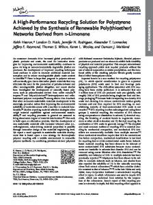
Fig. 1. Systolic computational-memory array over a 2D FPGA array.
Fig. 2. Pipelined data-path of PE.
As we reported in [11], we implemented a 2D systolic computational-memory array (SCMA) with a single FPGA, and mapped the neighboring accumulations of computational fluid dynamics (CFD) onto the array by decomposing the 2D computational grid into subgrids. The implemented SCMA achieved scalable performance to the number of PEs with a high efficiency. Thus we demonstrated the feasibility and scalability of the SCM architecture for CFD with a single FPGA. However, multiple-FPGA implementation was not considered, which is indispensable to further scale performance. Moreover, the computational generality of the SCM architecture was not demonstrated yet. In this paper, we generalize the SCMA for FPGA-based HPC by extending the target problem from only CFD to a group of numerical computations based on the difference schemes, and giving a framework to construct a scalable CCM upon multiple tightly-coupled FPGAs. For multiple-FPGA implementation, partitioning the array needs to be discussed: which part of the array should be implemented with each FPGA. We make a choice of homogeneous partitioning shown in Fig.1, where each FPGA takes charge of the sub-array partitioned uniformly. This is because the off-chip I/O bandwidth of future FPGAs will still remain insufficient for the computational memory architecture, while their logic elements, embedded memories and DSP blocks are growing with very wide internal bandwidth. As we discuss later, the communication between adjacent PEs requires much less bandwidth than the access of the local memory in each PE, which shows that our design choice is reasonable. Such homogeneous partitioning also gives high productivity by using each FPGA as a common module of the sub-array. Fig.1 shows the functional blocks and the controllers of PEs. We design the CCM composed of the hardware (HW) part with static configuration and the software (SW) part for dynamically controlling data-paths with microprograms to give computational generality and facility to the SCMA. Even if we use FPGAs, it is reasonable to share common HW components as much as possible for different problems because it takes long time to design and compile the HW part. Therefore, we implement the computing units, the data-paths and the network as the HW part in CCMs, though they are specialized for the target problem. Next, in order to achieve various computations with the HW
part, we employ sequencers to control the data-paths with our defined microprograms. The software given by these microprograms forms the dynamic part of our CCMs. This is a software, but not almighty and not too flexible. It is so simple that only necessary functions are defined just enough for the so-called time-sharing implementation of static functions on a limited hardware. Thanks to this approach, we can use common units for various computations, and consequently achieve high utilization of them, which is very important for HPC with limited HW resources. The programmability also allows us to easily develop CCMs for different computing problems. The complex and specialized computations such as boundary computations can also be performed with the same HW part by having the dynamic SW layer. Thus, almost all the computations of a problem can be performed independently of a host machine. C. Design In this section, we summarize our design criteria of the SCMA, and describe an actual design in HW and SW aspects. C.1 Hardware part Although the computations based on the difference scheme are commonly comprised of the neighboring accumulations of Eq.(2), each accumulation has a different number of terms with different constants. Therefore if we implement a fixed data-path for accumulating a fixed number of terms, it results in lower utilization of units for a different number of terms. To achieve high utilization, we sequentially use a MAC (Multiplication and ACcumulation) unit for the accumulation of any number of terms. Moreover, since the accumulation results are often used for the computations at the adjacent grid-points, we designed the datapath so that the output of the MAC unit can be directly transferred to the adjacent PEs. Fig.2 show the data-path of the PE, which has logically the same functions as those for a single FPGA implementation reported in [11]. The data-path is composed of a sequencer, a local memory and a MAC unit. The local memory stores all the necessary data for the sub-gird allocated to the PE, and temporal or intermediate results of computations. The sequencer controls the programmable PEs. The sequencer has a sequence memory to store a microprogram, and a program counter (PC) to specify a microinstruction output to the remaining data-path. Since all
TABLE I D EFINED MICROPROGRAMS OF PROCESSING ELEMENT. Opcode Dst1, Dst2,
Src1,
Src2
mulp
-,
L1,
SFIFO,
L2
mulm
SN,
-,
L2,
L3
accp
-,
L1,
L2,
L3
nop halt lset
num, addr
bnz accpbnz
-, L1, L2, L3
Description MACout = 0 + SFIFO × M[L2], M[L1] := MACout MACout = 0 - M[L2] × M[L3], FIFOs of {S&N}-PEs := MACout, MACout = MACout + M[L2] × M[L3] M[L1] := MACout, No operation Halt the array processor. Loop-counter := num. Bnz-regi := addr (for i-th nested loop). Branch if loop-counter not eq. to zero. Execute accp and bnz simultaneously.
the numerical computations have loop structures for an iterative solver and time marching, we designed a hardwired loop-control mechanism including multiple loop counters for nested loops. Basically each sequencer is not dedicated to a PE, but multiple PEs share the one as mentioned above. The number of PEs sharing the same sequencer depends on a type of applications. The data-path is pipelined with eight stages: MS (Microoperation Sequence) stage, MR (Memory Read) stage, five EX (Execution) stages and WB (Write Back) stage, while the MAC unit occupies the five EX stages. The MAC unit performs multiplication and accumulation of floating-point numbers. In the accumulation mode, the MAC unit computes a × b with the two inputs of a and b, and then adds or subtracts ab with its output. For this accumulation, the MAC unit has a forwarding path from EX5 to EX2. This three-stage forwarding forces the inputs to be fed for accumulation every three cycles. This means that three sets of Eq.(2) have to be concurrently performed in order to fully utilize the multiplier and the adder of the MAC unit. The output of the MAC unit is written into the local memory, and/or sent to the adjacent PEs through the communication FIFOs (First-In First-Out queues). In the 2D mesh network of the array, each PE is connected to the four adjacent PEs with the north(N-), south(S-), west(W-) and east(E-) FIFOs. These FIFOs allow PEs to avoid too rigorous requirement for synchronization in sending and receiving data to/from the adjacent PEs. C.2 Software part To describe microprograms that perform numerical computations with the aforementioned HW part, we defined a assembly language based on the following requirements: 1. MAC unit takes two inputs from memory or FIFOs. 2. MAC unit multiplies, and then adds or accumulates. 3. Output of MAC unit is written to memory and/or FIFOs. 4. Computations are repeated by nested loops. Table I shows the microinstruction set of the PE, which is composed of computing instructions and controlling instructions. There is no comparison instruction and no conditional branch that are not necessary for our present target computations. The computing instruction takes an operation code (Opcode), two destinations (Dst1 and Dst2), and two sources (Src1 and Src2). The opcodes: mulp, mulm and accp are “multiply and add with zero”, “multiply and subtract with zero” and “multiply and accu-
1: 2: 3: 4: 5: 6: 7: 8: 9: 10: 11: 12: 13: 14: 15:
lset 1000, LOOP LOOP: mulp -, -, mulp -, -, mulp -, -, accp -, -, accp -, -, accp -, -, accp -, -, accp -, -, accp -, -, accp WS, F_0_0, accp , F_1_0, accpbnz ES, F_2_0, nop halt
WFIFO, F_0_0, F_1_0, SFIFO, SFIFO, SFIFO, F_0_1, F_1_1, F_2_1, F_1_0, F_2_0, EFIFO,
C_1 C_1 C_1 C_2 C_2 C_2 C_3 C_3 C_3 C_4 C_4 C_4
Fig. 3. Example of a microprogram.
mulate with the previous output”, respectively. The first destination, Dst1, specifies PEs where the computing result is sent. S, N, E and W of Dst1 correspond to the south PE, north PE, east PE and west PE, respectively. The second destination, Dst2, specifies the address of the local memory where the computing result is written. The first and second sources, Src1 and Src2, specify the addresses of the local memory or FIFOs from which values are read to the MAC unit. As controlling instructions, we have nop, halt, lset and bnz instructions. The lset and bnz instructions are dedicated to the nested loop control. The lset instruction is used to set a loopcounter and a jump-address register in the sequencer with num and addr, respectively. Then, when bnz is executed, the program counter is set to be the address stored in the jump-address register if the loop-counter is not equal to zero. Simultaneously, the loop-counter is decremented. Like the accpbnz instruction, the combination of a computing instruction and bnz simultaneously performs both the instructions at the same clock cycle. Fig.3 shows an example of a microprogram, which repeats the following accumulation 1000 times. f0,0 = c1 f−1,0 + c2 f0,−1 + c3 f0,1 + c4 f1,0
(3)
f1,0 = c1 f0,0
+ c2 f1,−1 + c3 f1,1 + c4 f2,0
(4)
f2,0 = c1 f1,0
+ c2 f2,−1 + c3 f2,1 + c4 f3,0
(5)
where c1 to c4 are constants, and fi, j is a value defined at point (i, j) of a 3×3 grid. In this example, we assume that f−1,0 , f0,−1 , f1,−1 , f2,−1 and f3,0 are not the data of this PE. f−1,0 and f3,0 are sent from the west PE and the east PE, respectively, while f0,−1 , f1,−1 and f2,−1 are sent from the south PE. D. I/O bandwidth requirement for FPGA-array To obtain scalable performance, we adopt the approach that we implement a large SCMA with multiple FPGAs by homogeneously partitioning the entire array as shown in Fig.1. In the multiple-FPGA implementation, the required communication bandwidth between adjacent FPGAs has to be less than the I/O bandwidth of the FPGA. Since the wider bandwidth is required for the higher computational performance of the subarray implemented on an FPGA, we have to limit the performance if the FPGA does not have enough I/O bandwidth for the requirement. In this subsection, we model the required band-
W MAX = 2NPE bf [Mbits/s]
North FPGA
Stratix II FPGA-A
2bf [Mbits/s]
Link
PE
PE
PE LVDS
West FPGA
East FPGA
FPGA
PE
PE
South FPGA FPGA array
Stratix II FPGA-B
Ngrid points
Systolic Array (12x8 PEs)
PE
Sub-array on an FPGA (NPE x NPE PEs)
Sub-grid on a PE (Ngrid x Ngrid points)
PCI Controller PCI Bus
addr data
control sequences
4.98GB/s
LVDS
SER
SER
Tx, Rx DES
Tx, Rx DES
data
Array Controller with 9 Sequencers
4.98GB/s
control sequences
data
Array Controller with 9 Sequencers upper-left
upper-right
Systolic Array (12x8 PEs) upper lower internal lower-left
left right
lower-right
Fig. 4. Bandwidth requirement of a 2D sub-array on an FPGA.
Fig. 5. Implemented SCMA with the two StratixII FPGAs.
width of each FPGA for scalability evaluation that will be described in the next section. As shown in Fig.4, we suppose that each FPGA contains the sub-array of NPE × NPE PEs, which is connected to the north, south, west and east FPGAs. Let b denote the number of bits of data that a PE can send to the adjacent one at each cycle. For the single-precision floating point numbers, b is 33 bits including 1 bit for the write control of FIFOs. When PEs operate at f MHz, the maximum bidirectional bandwidth in Mbits/s required for one side of the sub-array, WMax , is obtained as:
Stratix II EP2S180-5 FPGAs: FPGA-A and FPGA-B, DDR2 memories and a PCI controller. The host machine can access these FPGAs through the PCI bus. We wrote verilog codes and compiled them with QuartusII version 8.0 SP1. Fig.5 shows the overview of the implemented SCMA with 24 × 8 PEs in all. On each FPGA, we implement the 12 × 8 SCMA, the array controller including nine sequencers and the communication unit using LVDS (low voltage differential signaling) transceivers (Tx) and receivers (Rx), which are embedded units of a Stratix II FPGA. These embedded Tx and Rx provide x10 serialization and deserialization, resulting in 4.98 GByte/s for unidirectional bandwidth. Since we can implement one more LVDS communication unit on this Stratix II FPGA, it totally has the bidirectional I/O bandwidth of WFPGA = 4.98 × 4 = 19.92 GByte/s. In the present implementation, the size of a local memory on each PE is 2 KBytes where 512 single-precision floating-point numbers can be stored. The MAC unit contains an adder and a multiplier for single-precision floating-point numbers in the IEEE754 format except denormalized numbers. Each MAC unit is implemented with one embedded 36-bit multiplier. The four communication FIFOs of a PE each have 32 entries, which are enough for send/receive synchronization in microprograms. All the 36-bit multipliers are employed to implement 12 × 8 SCMA in each FPGA. The 96 PEs share the nine sequencers. The size of each sequence memory is 64 KBytes, where up to 8192 microinstructions can be stored. These nine sequencers are allocated to the 60 internal PEs, the 6 left PEs, the 6 right PEs, the 10 top PEs, the 10 bottom PEs, and the top-left PE, the top-right PE, the bottom-left PE and the bottom-right PE, respectively. This allocation is useful for different computations of the grid boundary. The implemented SCMA operates at f = 106 MHz, though further optimization is probably possible. Then each PE has 212 MFlops (= 106MHz × 2), and the sub-array on each FPGA provides 20.35 (= 0.212× 96) GFlops. The maximum bidirectional bandwidth required for the link between FPGA-A and FPGA-B is WMax = 2NPE b f = 2 × 8 × 33 × 106 = 55968 Mbits/s = 7.0 GByte/s. Since the implemented communication unit has the bidirectional bandwidth of 4.98 × 2 = 9.96 GByte/s for the link, the two FPGAs can fully operate at 106MHz with this sufficient inter-FPGA bandwidth. Accordingly, the double-sized array on the two FPGAs achieves the doubled peak performance of 40.7 (= 0.212 × 192) GFlops. We refer the 12 × 8 SCMA implemented with FPGA-A or
WMax = 2NPE b f .
(6)
We referred to the one communication channel between the adjacent two FPGAs as a link. WMax is the maximum bandwidth required for each link. In the case of a 2D FPGA-array, 4WMax for the four links must be less than the total I/O bandwidth of the FPGA, WFPGA . However, actual computation does not require this full bandwidth, i.e., a microprogram does not have communication instructions at every cycle as shown in Fig.3. Let Icom be the smallest number of cycles between successive communication instructions, which is referred to as a minimum communication interval. In the case of Fig.3, Icom = 2 because of the 11th and 13th instructions sending data to the south-PE. Then the actual required bandwidth is given: Wactual =
WMax 2N b f = PE . Icom Icom
(7)
In the case of a 2D FPGA-array, the following bandwidth constraint is similarly applied. 4Wactual for the four links must be less than the total I/O bandwidth of the FPGA. 4Wactual ≤ WFPGA .
(8)
Obviously, large Icom , limits the bandwidth requirement for the I/O bandwidth constraint. IV. P ERFORMANCE E VALUATION In this section, we discuss the feasibility of our SCMA while evaluating the computational performance, the power consumption and scalability for available FPGA products through prototype implementation with two FPGAs. A. Implementation We implemented the SCMA with the FPGA prototyping board: DN7000k10PCI [32]. The board has two ALTERA
a. Red-black-SOR.
d. FDTD, time-step=120.
b. Fractional-step method, time-step=120.
e. FDTD, time-step=240.
c. Fractional-step method, time-step=4000.
f. FDTD, time-step=360.
g. FDTD, time-step=620.
Fig. 6. Computational results of the red-black-SOR (a), the fractional-step method (b and c), and the FDTD method (d to g). For the red-black-SOR, φ (temperature) is visualized in color. For the fractional-step method, the pressure per density and the velocity vectors are visualized. For the FDTD method, the norm of the electric field is visualized. TABLE II B ENCHMARK COMPUTATIONS . N grid-points
N grid-points
N grid-points
y x
u=0, v=0
M grid-points
u=0, v=0
M grid-points
u=0, v=0
u=uf , v=0
M grid-points
FPGA-B as the single-FPGA SCMA. From software, the 24 × 8 PEs implemented over FPGA-A and FPGA-B is also transparently seen as a single array, which is referred to as the doubleFPGA SCMA. These SCMAs have an idle mode and a computing mode. We use the idle mode to initialize all the local memories and write microprograms in the sequencers before computation, and read the computational results in the local memories after computation. To start the computation, we switch the mode to the computing mode.
Ex Ey wave source of Hz y (xs, ys)
Hz
Ey
Ex
x
Absorbing boundary condition
B. Benchmarks For a benchmark, we use the applications summarized in Table II. The red-black-SOR (successive over-relaxation) method [33], RB-SOR, is one of the iterative solvers for Poisson’s equation or Laplace’s equation. In the red-black-SOR method, the grid points are treated as a checkerboard with red and black points, and each iteration is split into red-step and black-step. The red- and black-steps compute the red points and the black points, respectively. We solve the heat-conduction problem on a 2D square plate shown in Table II by solving the Laplace’s equation. For the single-FPGA SCMA and the double-FPGA SCMA, we compute 3.0 × 10⁵ iterations with a 96 × 192 grid, and 1.5 × 10⁵ iterations with a 192 × 192 grid, respectively, where PEs each take charge of a 8 × 24 sub-grid in both the cases. Fig.6a shows the computational result of the converged solution for the 192 × 192 grid. The fractional-method [34, 35], Frac, is a typical and widelyused numerical method for computing incompressible viscous flows by numerically solving the Navier-Stokes equations. We compute the 2D square driven cavity flow as shown in Table II. The left, right and lower walls of the square cavity are stable, and only the upper surface is moving to right with a velocity of u = 1.0. For the single-FPGA SCMA and the double-FPGA SCMA, we compute 8000 time-steps with a 48 × 48 grid, and 4000 time-steps with a 96 × 48 grid, respectively, where PEs
Red-black-SOR
Fractional-step method
FDTD method
Numerical method to Iterative numerical Numerical method to solve Maxwell’s equasolver of Laplace’s compute incompressible tions for electromagnetic 2 equation: ∇ φ = 0. viscous flow. problems.
each is in charge of a 4 × 6 sub-grid in both the cases. In each time-step, we solve the Poisson’s equation with 250 iterations of the Jacobi method. The computation finally causes a vortex flow in the square cavity as shown in Figs.6b and 6c. The finite-difference time-domain (FDTD) method [36, 37], FDTD, is a powerful and widely-used tool to solve a wide variety of electromagnetic problems, which provides a direct timedomain solution of Maxwell’s Equations discretized by difference schemes on a uniform grid and at time intervals. We compute the 2D electromagnetic-wave propagation as shown in Table II. At the left-bottom corner, we put the square-wave source with the amplitude of 1 and the period of 80 time-steps. On the border, Mur’s first-order absorbing boundary condition is applied. For the single-FPGA SCMA and the double-FPGA SCMA, we compute 5.6 × 10⁵ time-steps with a 72 × 72 grid, and 2.8 × 10⁵ time-steps with a 144 × 72 grid, respectively, where PEs each is in charge of a 6 × 9 sub-grid in both the cases. Figs.6d to 6g show the computed time-dependent results.
TABLE III P ERFORMANCE , POWER AND ENERGY RESULTS . Pentium4 (3.4GHz)
SCMA (106MHz)
time[s]
power[W]
energy[J]
RB-SOR (96 × 192, 300000)
31.30
-
-
Frac. step (48 × 48, 8000)
33.69
125.73
4222.4
FDTD (72 × 72, 560000)
31.78
125.99
4009.9
RB-SOR (192 × 192, 150000)
31.03
-
-
Frac. step (96 × 48, 4000)
33.92
125.91
4229.8
FDTD (144 × 72, 280000)
32.00
125.95
4038.5
FPGA(s) single (96 PEs) double (192 PEs)
For comparison, we wrote programs of these benchmarks in C to be executed on a Linux host PC, hp ProLiant ML310 G3, with Intel Pentium4 processor model 550 operating at 3.4GHz. All the floating-point computations are performed in single precision. We compiled the programs using gcc with “-O3” option, and measured the execution time of the core computation, which is the same part as those executed by FPGAs, with gettimeofday() system call. For FPGA-based computation, we wrote sequences for the benchmark computations. As shown in Fig.5, the sub-array implemented on each FPGA has nine sequencers, which are allocated to the following PE groups containing: the upper, the lower, the left, the right boundaries, the upper-left, the upperright, the lower-left, the lower-right corners and the internal grid-points, respectively, because they need different sequences for different boundary computations. The FPGA-based computation and the software computation with the Pentium4 processor give almost the same results for the benchmarks. C. Performance evaluation of the implemented SCMAs Table III shows the performance results of the 3.4GHz Pentium4 processor and the 106MHz FPGA-based SCMAs. For both the single-FPGA SCMA and the double-FPGA SCMA, we count the number of cycles executed by each PE and calculate the exact execution time. For RB-SOR, Frac and FDTD, the utilization of the MAC unit is around 90%, 88% and 80%, respectively. Although about 10 to 20% loss of utilization is caused by the first input for the neighboring accumulation of Eq.(2), the customized data-path allows applications to enjoy these high utilizations. These MAC utilizations give RB-SOR, Frac and FDTD the sustained performances of 18.2 GFlops, 17.8 GFlops and 16.3 GFlops, respectively, for the single-FPGA SCMA. The double-FPGA SCMA achieves 36.5 GFlops, 35.7 GFlops and 32.8 GFlops, respectively. These sustained performances obviously exceed the peak single-precision performance of the 3.4GHz Pentium4 processor: 13.6 GFlops given by SSE3 (streaming SIMD extension 3) instructions. On the contrary, gcc does not fully utilize the peak performance at all. Consequently, the double-FPGA SCMA provides 20 to 29 times faster computation than the Pentium4 processor, though an advanced compiler like icc may give better performance to the Pentium4 processor. Note that the MAC utilization is kept almost the same for the single-FPGA SCMA and the double-FPGA SCMA. This
MAC util. GFlops
speedup
power[W]
89.5%
18.2
288000039
2.717
11.52
-
-
87.6%
17.8
245512041
2.316
14.55
86.56
200.12
total cycles time[s]
energy[J]
282.46
80.2%
16.3
332668023
3.138
10.13
90.21
89.6%
36.5
144000039
1.358
22.85
-
-
87.7%
35.7
122756041
1.158
29.3
101.17
117.03
80.6%
32.8
166334023
1.569
20.4
109.81
171.96
AC 100V
HDD 80GB hp ProLiant ML310 G3
benchmark (grid,iter)
Power Supply Unit
HDS728080 PLA380
SATA
DC +3.3V, +5V, +12V
DC voltage
Memory HiCorder HIOKI 8855
DC current
Main Board Chipset: Intel E7230 Intel Pentium4 550 3.4GHz PC4200 DDR2 2GB On-board Graphics, GbE
PCI
FPGA Board DN7000K10PCI StratixII EP2S180
Fig. 7. Power measurement of the host PC and the SCMA. All the DC inputs to the main board are measured.
means that FPGAs with sufficient I/O bandwidth provide complete scalability with high utilization of the units. Generally, parallel computers employing a lot of processors have difficulty in keeping such high efficiency. D. Power consumption We evaluate the actual power and energy consumption of the SCMAs compared to the software computation. To obtain the power consumption, we use a digital oscilloscope, HIOKI Memory HiCorder 8855, which can measure and record samples of DC voltage and current of input channels. Fig.7 shows the power measurement of the host PC and the FPGA prototyping board. We measure the DC inputs to the main board: DC +3.3V, DC +5V and DC +12V. The sampling rate is 1.0 × 10³ samples/sec. the digital oscilloscope also calculates the power with the measured voltage and current. Thus, we can observe the net power consumption of the system including the chipset, the CPU, the main memories, the other peripherals and the FPGAs. Table III summaries the average power and the total energy for Frac and FDTD by the Pentium4 processor whose TDP is 115W and the SCMAs. The SCMAs consume the 70% to 87% power of that by the Pentium4 processor, and their computational speedup allows the SCMAs to require only 3% to 7% of the total energy for the Pentium4 processor. Note that the total energy for the double-FPGA SCMA is less than that for the single-FPGA SCMA while the Pentium4 processor consumes almost the same energy for these benchmarks. This shows that net energy consumption for FPGAs is very low. If we use ten FPGAs with a single host PC, their energy consumption is much smaller than that for the ten PCs. Thus our FPGA-based SCMA has the advantage of much low power/energy-consumption especially for higher performance.
TABLE IV E STIMATION OF ARRAY SIZE AND REQUIRED BANDWIDTH BASED ON HARDWARE RESOURCES OF AVAILABLE FPGA S .
LEs Memory [KBytes] 36-bit DSPs LVDS ch(Tx,Rx each) BW per ch [MB/s] Total bidir BW [GB/s] PE freq [MHz] Estimated # of PEs Peak GFlops 4WMax [GB/s] 4Wactual [GB/s] (Icom = 6)
StratixIV E EP4SE680 681,100 3,936 340 132 200 52.8 106 340 72.1 64.5 10.8
StratixIII L EP3SL340 337,500 2,034 144 132 156.25 41.3 106 144 30.5 42.0 7.0
StratixII CycloneIII EP2S180 EP3C120 179,400 119,088 1,145 486 96 288/4 156 110 125 80 39 17.6 106 106 96 72 20.3 15.3 34.3 29.7 5.7
4.9
However the actual bandwidth requirement can be lower for real applications. The minimum communication intervals, Icom , has the order of O(Ngrid Ninst ) where the sub-grid size is Ngrid 2 and each grid-point takes Ninst instructions. For RB-SOR, Frac and FDTD, their microprograms give Icom of 30, 9 and 18, respectively, for the west or east direction. These values almost agree with O(Ngrid Ninst ) where Ngrid = 8, 4 and 6, and Ninst = 5, 3 and 3, respectively. Like these examples, we think that real computations have Icom > 22 , considering their Ngrid and Ninst . If we assume that Icom ≥ 6, all the FPGAs sufficiently satisfy the condition that 4Wactual ≤ WFPGA . This result means that our SCMA has complete scalability with multiple FPGAs arranged in a 2D array for real computing problems. Note that the required bandwidth, WMax , does not grow so much as the peak performance of each FPGA does. This is because the performance is O(NPE 2 ) while the required bandwidth is O(NPE ). Thus our strategy to homogeneously partition an SCMA over FPGAs is practical and useful for currently available and future FPGAs with such balanced I/O and logic/DSPs.
E. Feasibility of a large SCMA with available FPGAs In the present implementation of Fig.5, the double-FPGA SCMA achieves the doubled performance of that of the singleFPGA one due to the total I/O bandwidth, WFPGA , higher than the maximum bidirectional bandwidth for the link, WMax (or Wactual for Icom = 1). Here we discuss the feasibility of SCMAs over a 2D FPGA array in terms of their I/O bandwidth through estimating bandwidth requirement for commercially available FPGAs. Table IV shows examples of high-end and low-end FPGAs of different generations, and their hardware specifications [38]: the number of LE (logic elements), the total size of embedded memories in KBytes, the number of 36-bit DSP blocks, the number of LVDS channels for Tx and Rx each, and the bandwidth per LVDS channel. For CycloneIII, we estimated the number of 36bit DSP blocks by dividing the number of 18-bit DSP blocks with 4. We obtained the total bidirectional bandwidth of FPGA I/O by calculating 2NLVDS-chWLVDS-ch , where NLVDS-ch is the number of LVDS channels for Tx and Rx each, and WLVDS-ch is the unidirectional bandwidth per channel. In this table, StratixII EP2S180 has higher I/O bandwidth than that of our implementation because the FPGA prototyping board uses the I/O pins not only for the inter-FPGA connection, but also for the on-board memory and the PCI interface. We assume that single-precision floating-point numbers are used where b = 33, and the same frequency as f = 106MHz can be achieved for SCMAs on these FPGAs. We estimate the number of PEs implemented on an FPGA, NPE 2 , with the number of 36-bit DSP blocks. Then we obtained the maximum bidirectional-bandwidth required for one link, WMax , with 2NPE b f /8000 GByte/s. For a 2D FPGA-array, the total required bandwidth is 4WMax because each FPGA has four links. Under these assumption and estimation, the Stratix series of ALTERA’s high-end FPGAs have the I/O bandwidth close to the required one, 4WMax , while the low-end CycloneIII FPGA has almost half of the required bandwidth. This means that the high-end FPGAs have well-balanced I/O bandwidth with their computing performance, while the low-end one does not.
V. C ONCLUSIONS In this paper, we have proposed the scalable FPGA-array to achieve custom computing machines for high-performance and power-efficient scientific simulations based on difference schemes. By introducing the homogeneous partitioning, we allow a systolic computational-memory array (SCMA) to be extensible over an array of multiple tightly-coupled FPGAs. A large SCMA implemented using a lot of FPGAs achieves highperformance computation with scalable memory-bandwidth and scalable arithmetic-performance. For feasibility demonstration and quantitative evaluation, we designed and implemented the SCMA of 24 × 8 = 192 PEs with the two StratixII FPGAs on the same board. The SCMA operates at 106MHz, and the implemented communication units using LVDS provide sufficient inter-FPGA bandwidth for the SCMA to fully perform computations. The two FPGAs have the peak performance of 40.7 GFlops of single-precision floatingpoint computations, while each FPGA has the half of the performance. The double-FPGA SCMA achieves the sustained performance of 32.8 to 36.5 GFlops with high utilization of MAC units for the benchmark computations. In comparison with the 3.4GHz Pentium4 processor, the SCMAs demonstrate much higher power-efficiency: 70% to 87% power consumption and only 3% to 7% energy consumption for the same computations. We also discussed the scalability of SCMAs with a 2D FPGAarray. We formulated the bandwidth requirement model with the communication frequency in a computational program. Based on this model, we projected that SCMAs are completely scalable for the currently available high-end to low-end FPGAs. The limited size of local memories on each FPGA is the problem of SCMAs. However, as shown in Table IV, favorably growing size of embedded memories of FPGAs will give better situation, while we are also expecting the DRAM/Logic merged technology to provide FPGAs much more embedded memories. Our future work includes 3D computation on a larger SCMA, more dedicated data-paths/networks of PEs to the target com-
putations, a sophisticated mechanism for accessing the SCMA’s memory, compilers for SCMAs and application of SCMAs to high-performance signal processing. For implementing a largerscale SCMA with multiple boards, we are planning to use stackable FPGA boards like ALTERA DE3 [38].
[16]
[17]
ACKNOWLEDGMENTS This research was supported by MEXT Grant-in-Aid for Young Scientists(B) No.20700040 and MEXT Grant-in-Aid for Scientific Research(B) No.19360078. We thank Professor Takayuki Aoki and Associate Professor Takeshi Nishikawa, Tokyo Institute of Technology, and Assistant Professor Hiroyuki Takizawa, Tohoku University, for power measurement.
[18]
[19]
[20]
R EFERENCES [1]
[2] [3]
[4] [5] [6]
[7]
[8]
[9]
[10]
[11]
[12]
[13]
[14]
[15]
Keith D. Underwood and K. Scott Hemmert, “Closing the gap: Cpu and fpga trends in sustainable floating-point blas performance,” Proceedings of the 12th Annual IEEE Symposium on Field-Programmable Custom Computing Machines, pp. 219–228, 2004. K. Underwood, “Fpga vs. cpus: Trends in peak floating-point performance,” Proceedings of the International Symposium on FieldProgrammable Gate Arrays, pp. 171–180, February 2004. Nabeel Shirazi, Al Walters, and Peter Athanas, “Quantitative analysis of floating point arithmetic on fpga based custom computing machines,” Proceedings of the IEEE Symposium on FPGA’s for Custom Computing Machines, pp. 155–162, 1995. Michael deLorimier and André DeHon, “Floating-point sparse matrixvector multiply for fpgas,” Proceedings of the International Symposium on Field-Programmable Gate Arrays, pp. 75–85, February 2005. Ling Zhuo and Viktor K. Prasanna, “Sparse matrix-vector multiplication on fpgas,” Proceedings of the International Symposium on FieldProgrammable Gate Arrays, pp. 63–74, February 2005. Yong Dou, S. Vassiliadis, G. K. Kuzmanov, and G. N. Gaydadjiev, “64bit floating-point fpga matrix multiplication,” Proceedings of the International Symposium on Field-Programmable Gate Arrays, pp. 86–95, February 2005. James P. Durbano, Fernando E. Ortiz, John R. Humphrey, Petersen F. Curt, and Dennis W. Prather, “Fpga-based acceleration of the 3d finitedifference time-domain method,” Proceedings of the 12th Annual IEEE Symposium on Field-Programmable Custom Computing Machines, pp. 156–163, April 2004. Chuan He, Mi Lu, and Chuanwen Sun, “Accelerating seismic migration using fpga-based coprocessor platform,” Proceedings of the 12th Annual IEEE Symposium on Field-Programmable Custom Computing Machines, pp. 207–216, April 2004. Chuan He, Wei Zhao, and Mi Lu, “Time domain numerical simulation for transient waves on reconfigurable coprocessor platform,” Proceedings of the 13th Annual IEEE Symposium on Field-Programmable Custom Computing Machines, pp. 127–136, April 2005. Ronald Scrofano, Maya B. Gokhale, Frans Trouw, and Viktor K. Prasanna, “A hardware/software approach to molecular dynamics on reconfigurable computers,” Proceedings of the 14th Annual IEEE Symposium on FieldProgrammable Custom Computing Machines, pp. 23–34, April 2006. Kentaro Sano, Takanori Iizuka, and Satoru Yamamoto, “Systolic architecture for computational fluid dynamics on fpgas,” Proceedings of the 15th Annual IEEE Symposium on Field-Programmable Custom Computing Machines (FCCM2007), pp. 107–116, April 2007. Ling Zhuo and Viktor K. Prasanna, “Scalable and modular algorithms for floating-point matrix multiplication on reconfigurable computing systems,” IEEE Transactions on Parallel and Distributed Systems, vol. 18, no. 4, pp. 433–448, April 2007. Ling Zhuo, Gerald R. Morris, and Viktor K. Prasanna, “High-performance reduction circuits using deeply pipelined operators on FPGAs,” IEEE Transactions on Parallel and Distributed Systems, vol. 18, no. 10, pp. 1377–1392, October 2007. K. Scott Hemmert and Keith D. Underwood, “An analysis of the doubleprecision floating-point fft on fpgas,” Proceedings of the 13th Annual IEEE Symposium on Field-Programmable Custom Computing Machines, pp. 171–180, April 2005. Gerald R. Morris, Viktor K. Prasanna, and Richard D. Anderson, “A hybrid approach for mapping conjugate gradient onto an FPGA-augmented reconfigurable supercomputer,” Proceedings of the 14th Annual IEEE
[21] [22] [23]
[24]
[25]
[26] [27] [28]
[29]
[30]
[31]
[32] [33] [34] [35] [36] [37] [38]
Symposium on Field-Programmable Custom Computing Machines, pp. 30–12, April 2006. Richard L. Walke, Robert W. M. Smith, and Gaye Lightbody, “20GFLOPS QR processor on a xilinx virtex-e FPGA,” Proceedings of SPIE: Advanced Signal Processing Algorithms, Architectures and Implementations X, vol. 4116, pp. 300–310, June 2000. Arun Patel, Christopher A. Madill, Manuel Saldana, Christopher Comis, Regis Pomes, and Paul Chow, “A scalable FPGA-based multiprocessor,” Proceedings of the 14th Annual IEEE Symposium on Field-Programmable Custom Computing Machines, pp. 111–120, April 2006. Ronald Scrofano, Maya B. Gokhale, Frans Trouw, and Viktor K. Prasanna, “Accelerating molecular dynamics simulations with reconfigurable computers,” IEEE Transactions on Parallel and Distributed Systems, vol. 19, no. 6, pp. 764–778, June 2008. Alexander Kaganov, Paul Chow, and Asif Lakhany, “FPGA acceleration of monte-carlo based credit derivative pricing,” Proceedings of the International Conference on Field Programmable Logic and Applications, pp. 329–334, September 2008. Nathan A. Woods and Tom VanCourt, “FPGA acceleration of quasi-monte carlo in finance,” Proceedings of the International Conference on Field Programmable Logic and Applications, pp. 335–340, September 2008. T. Hauser, “A flow solver for a reconfigurable fpga-based hypercomputer,” AIAA Aerospace Sciences Meeting and Exhibit, 2005. William D. Smith and Austars R. Schnore, “Towards an rcc-based accelerator for computational fluid dynamics applications,” The Journal of Supercomputing, vol. 30, no. 3, pp. 239–261, December 2003. Ryan N. Schneider, Laurence E. Turner, and Michal M. Okoniewski, “Application of fpga technology to accelerate the finite-difference timedomain (FDTD) method,” Proceedings of the 2004 ACM/SIGDA 12th international symposium on Field programmable gate arrays (FPGA2002), pp. 97–105, Febuary 2002. Wang Chen, Panos Kosmas, Miriam Leeser, and Carey Rappaport, “An fpga implementation of the two-dimensional finite-difference time-domain (FDTD) algorithm,” Proceedings of the 2004 ACM/SIGDA 12th international symposium on Field programmable gate arrays (FPGA2004), pp. 213–222, Febuary 2004. Tsutomu Hoshino, Toshio Kawai, Tomonori Shirakawa, Junichi Higashino, Akira Yamaoka, Hachidai Ito, Takashi Sato, and Kazuo Sawada, “Pacs: A parallel microprocessor array for scientific calculations,” ACM Transactions on Computer Systems, vol. 1, no. 3, pp. 195–221, 1983. H. T. Kung, “Why systolic architecture?,” Computer, vol. 15, no. 1, pp. 37–46, 1982. Kurtis T. Johnson, A.R. Hurson, and Behrooz Shirazi, “General-purpose systolic arrays,” Computer, vol. 26, no. 11, pp. 20–31, 1993. J. E. Vuillemin, P. Bertin, D. Roncin, M. Shand, H. H. Touati, and P. Boucard, “Programmable active memories: reconfigurable systems come of age,” IEEE Transactions on Very Large Scale Integration (VLSI) Systems, vol. 4, no. 1, pp. 56–69, Mar 1996. David Patterson, Krste Asanovic, Aaron Brown, Richard Fromm, Jason Golbus, Benjamin Gribstad, Kimberly Keeton, Christoforos Kozyrakis, David Martin, Stylianos Perissakis, Randi Thomas, Noah Treuhaft, and Katherine Yelick, “Intelligent ram(iram): the industrial setting, applications, and architectures,” Proceedings of the International Conference on Computer Design, pp. 2–9, October 1997. David Patterson, Thomas Anderson, Neal Cardwell, Richard Fromm, Kimberly Keeton, Christoforos Kozyrakis, Randi Thomas, and Katherine Yelick, “A case for intelligent ram: Iram,” IEEE Micro, vol. 17, no. 2, pp. 34–44, March/April 1997. Duncan G. Elliott, Michael Stumm, W.Martin Snelgrove, Christian Cojocaru, and Robert Mckenzie, “Computational ram: Implementing processors in memory,” Design & Test of Computers, vol. 16, no. 1, pp. 32–41, January-March 1999. The Dini Group, “http://www.dinigroup.com/,” 2008. Louis A. Hageman and David M. Young, Applied Iterative Methods, Academic Press, 1981. J. Kim and P. Moin, “Application of a fractional-step method to incompressible navier-stokes,” Journal of Computational Physics, vol. 59, pp. 308–323, June 1985. John C. Strikwerda and Young S. Lee, “The accuracy of the fractional step method,” SIAM Journal on Numerical Analysis, vol. 37, no. 1, pp. 37–47, November 1999. Kane S. Yee, “Numerical solution of inital boundary value problems involving maxwell’s equations in isotropic media,” IEEE Transactions on Antennas and Propagation, vol. 14, pp. 302–307, May 1966. Taflove Allen and Hagness Susan C., Computational electrodynamics The finite difference time-domain method, Norwood, MA: Aretch House Inc., 1996. Altera Corporation, “http://www.altera.com/literature/,” 2008.