AbstractâIn this paper, a new single-stage input-cur- rent-shaping (S2ICS) technique that integrates the voltage-dou- bler-rectifier front end with a dc/dc output ...
IEEE TRANSACTIONS ON POWER ELECTRONICS, VOL. 16, NO. 1, JANUARY 2001
55
Single-Stage Input-Current-Shaping Technique with Voltage-Doubler-Rectifier Front End Jindong Zhang, Student Member, IEEE, Laszlo Huber, Member, IEEE, Milan M. Jovanovic´, Fellow, IEEE, and Fred C. Lee, Fellow, IEEE
Abstract—In this paper, a new single-stage input-current-shaping (S2 ICS) technique that integrates the voltage-doubler-rectifier front end with a dc/dc output stage is introduced. Due to the voltage-doubler-rectifier front end, a reduction of line-current harmonics can be achieved with a higher conversion efficiency compared to the corresponding S2 ICS circuit with the conventional wide-range full-bridge rectifier. The proposed technique requires energy-storage capacitors with the same total capacitance and with half of the voltage rating as in the conventional S2 ICS counterpart, which reduces the size and cost of the power supply. The performance of the proposed technique is evaluated on a 450-W (5-V/ 90-A) experimental prototype circuit. Index Terms—Line current shaper, power factor correction, single-stage ac–dc conversion, voltage-doubler rectifier.
I. INTRODUCTION
A
number of single-stage input-current-shaping (S ICS) techniques have been introduced recently. In a single-stage approach, input current shaping (ICS), isolation, and high-bandwidth control are performed in a single step, i.e., without creating a regulated intermediate dc bus. Generally, S ICS circuits meet European and/or Japanese regulatory requirements regarding line current harmonics, but they do not improve the power factor (PF) and reduce the total harmonic distortion (THD) as much as their conventional two-stage counterparts. Typically, PF for S ICS circuits is between 0.8 and 0.9, whereas their THD is in the 40–75% range. Among the single-stage circuits, a number of circuits described in [1]–[12] seem particularly attractive because they can be implemented with only one semiconductor switch and a simple control. All these S ICS circuits integrate a boost ICS stage with a forward or flyback dc/dc-converter stage. Although it has been demonstrated that the S ICS circuits described in [1]–[12] can achieve the desired performance in a variety of applications, the S ICS power supplies have significant difficulties meeting performance expectations in universal-line (90–270-Vac) applications with a hold-up time requirement. For example, most of today’s desktop computers and computer peripherals require power supplies that are capable of operating in the 90–270-Vac range and can provide a hold-up time of at least 10 ms. Generally, the hold-up time is the time during which a Manuscript received May 27, 1999; revised September 26, 2000. Recommended by Associate Editor J. Thottuvelil. J. Zhang and F. C. Lee are with the Center for Power Electronics Systems, The Bradley Department of Electrical Engineering, Virginia Polytechnic Institute and State University, Blacksburg, VA 24060-0111 USA. L. Huber and M. M. Jovanovic´ are with the Delta Products Corporation, Power Electronics Laboratory, Research Triangle Park, NC 27709 USA. Publisher Item Identifier S 0885-8993(01)00980-2.
power supply must maintain its output voltage(s) within a specified range after a drop-out of the line voltage. The hold-up time is used to orderly terminate the operation of a computer or to switch over to an uninterruptible-power-supply (UPS) operation after a line failure. The required energy to support the output during the hold-up time is obtained from a properly sized en, which is used to handle the differergy-storage capacitor, ences between a varying instantaneous input power and a constant output power. The difficulty of these S ICS circuits to deal with a wide line range and long hold-up time requirement stems from the fact that the voltage of the energy-storage ca, varies with the line voltage and load current [4]. In pacitor, can be kept in the most applications, with a proper design, 410–420 Vdc range, which warrants the use of a 450-V elecis determined from the trolytic capacitor. Since the value of hold-up time requirement at the minimum line (worst case), the S ICS approach requires a relatively bulky and expensive energy-storage capacitor. Moreover, due to a wide-range variation , which is the input to the dc/dc output stage, the converof sion efficiency of the dc/dc output stage is reduced. In contrast, is independently regulated the two-stage approach, in which at approximately 380 Vdc, requires a much smaller and, therefore, cheaper electrolytic capacitor rated at 450 V, or even 400 V. , the efficiency of the dc/dc In addition, due to a regulated output stage in the two-stage approach can be made higher compared to that in the single-stage approach. Generally, the performance of conventional, universal-line-range power supplies without ICS can be improved by employing a voltage-doubler rectifier (VDR) [13]. The output voltage of a VDR front end is approximately the same for both the low-line range (90–135 Vac) and the high-line range (180–270 Vac), i.e., it varies from approximately Vdc to Vdc. Since this voltage range is half of the corresponding voltage range of the conventional wide-range full-bridge rectifier (FBR), the conversion efficiency of the dc/dc output stage can be improved. In addition, because the minimum voltage of the VDR is twice as high as that of the wide-range FBR, the total capacitance required for a given hold-up-time specification is approximately the same as the capacitance required in the wide-range FBR. However, the capacitors in the VDR need to be rated at only 250 Vdc, or even 200 Vdc. Usually, electrolytic capacitors with a lower voltage rating are significantly cheaper than their counterparts with a higher voltage rating. In this paper, a new S ICS technique that integrates the voltage-doubler-rectifier front end with a dc/dc output stage is introduced. First, in Section II, the S ICS technique with the conventional wide-range FBR is reviewed. The S ICS converters with the wide-range FBR can be classified in two
0885–8993/01$10.00 © 2001 IEEE
56
IEEE TRANSACTIONS ON POWER ELECTRONICS, VOL. 16, NO. 1, JANUARY 2001
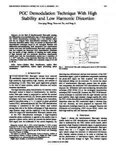
Fig. 1. S ICS circuits with three-terminal ICS cells: (a) DCM ICS cell with winding ICS cell [11], [12], and (d) capacitive CCM ICS cell [3].
families: the S ICS family with two-terminal ICS cells and the S ICS family with three-terminal ICS cells. In this paper, these two S ICS families were also extended to the voltage-doubler S ICS (VDS ICS) converter implementations: the VDS ICS family with two-terminal ICS cells and the VDS ICS family with three-terminal ICS cells. In Section III, generalized circuit diagrams and principles of operation for both the VDS ICS family with two-terminal ICS cells and the VDS ICS family with three-terminal ICS cells are presented. Finally, experimental results obtained on a 450-W (5-V/90-A) prototype circuit are given in Section IV. II. REVIEW OF S ICS CONVERTERS WITH WIDE-RANGE FBR Generally, the S ICS converters can be classified in two families: the S ICS family with two-terminal ICS cells and the S ICS family with three-terminal ICS cells. Although topologically different, the two S ICS families are functionally equivalent and exhibit very similar performance. The ICS inductor of a S ICS circuit with two-terminal or three-terminal ICS cells can operate either in the discontinuous conduction mode (DCM) or in the continuous conduction mode (CCM). In the DCM operation of the ICS inductor, low line-current harmonic distortions are achieved because of the inherent property of the DCM boost converter to draw a near sinusoidal current if its duty cycle is held relatively constant during a half line cycle. Generally, the DCM operation gives a lower THD of the line current compared to the CCM operation. However, the CCM operation yields a slightly higher efficiency compared to the DCM operation. A. S ICS Family with Three-Terminal ICS Cells A typical S ICS circuit with DCM operation of the ICS inductor is shown in Fig. 1(a) [7]. The ICS cell, shown in the and dotted rectangle in Fig. 1(a), consists of ICS inductor for charging when switch is two current paths: path
N
[7], (b) DCM ICS cell with windings
N
and
N
[8], (c) inductive CCM
on and path for discharging when switch is off. Since is connected to switch and discharging charging path is connected to energy-storage capacitor , the ICS path cell in Fig. 1(a) has three terminals. The function of the transin path is to limit the voltage on enformer winding and to improve the overall efficiency. ergy-storage capacitor also introduces line-current distortions However, winding around the zero crossings because the line current cannot flow when the instantaneous line voltage is lower than the voltage . Therefore, in the S ICS circuit in induced across winding Fig. 1(a) there is a strong trade-off between PF, THD, and efficiency. To further reduce the energy-storage capacitor voltage , can and improve efficiency, another transformer winding, as shown in Fig. 1(b) [8]. be placed in discharging path During the discharging of the ICS inductor, the voltage across has the same direction as the voltage across the windings effectively increases energy-storage capacitor, i.e., winding the reset voltage across the ICS inductor. As a result, the recan be obtained with a lower voltage quired reset voltage for . It should be noted that since on energy-storage capacitor and are magnetically coupled to the secondary windings , they can be used to directly transfer winding of transformer provides energy from the input (line) to the load. Winding direct energy transfer with the forward-type dc/dc power stages, provides direct energy transfer with the flywhile winding back-type dc/dc power stages. Generally, direct energy transfer improves the conversion efficiency. To achieve CCM operation of the ICS inductor, an additional inductor or capacitor is required as shown in Fig. 1(c) [11], [12] in and Fig. 1(d) [3], respectively. The function of inductor in Fig. 1(d) is to provide a variable Fig. 1(c) and capacitor even when the duty effective duty cycle for boost inductor cycle of switch is relatively constant during a half line cycle. Namely, to achieve a good tracking of the line current and line operating in CCM, it is necesvoltage with boost inductor , , defined as the ratio of the sary that the duty cycle of
ZHANG et al.: SINGLE-STAGE INPUT-CURRENT-SHAPING TECHNIQUE
57
charging time of and the switching period, is proportional to the instantaneous line voltage during a half line cycle. Specifishould be maximum around the zero crossings of the cally, line voltage and minimum around the line voltage peaks, i.e., (1) in Fig. 1(c) modulates boost-inductor duty cycle Inductor by delaying the commutation of the boost inductor curto path after switch is turned on. rent from path Since during this commutation time, which is proportional to continues the line current and, therefore, to the line voltage, varies with the line voltage even to discharge, duty cycle though the duty cycle of switch is relatively constant. Simimodulates by speeding up larly, in Fig. 1(d), capacitor to the commutation of the boost-inductor current from path after switch is turned on. Namely, after switch is path until turned on, boost-inductor current charges capacitor is charged to . Once is charged to , the boost-inductor . As a result, duty cycle current commutates to path is different from the duty cycle of switch . Furthermore, since is proportional to the boost-inductor the charging time of varies with the line voltage as shown in (1). current, In all S ICS circuits in Fig. 1, the three-terminal ICS cell, shown in the dotted rectangle, has the same basic topology that connected to the output of the fullincludes ICS inductor charging path connected to switch S, bridge rectifier, discharging path connected to energy-storage caand . Therefore, all S ICS circuits in Fig. 1 can be reppacitor resented by a S ICS circuit with a generalized three-terminal ICS cell as shown in Fig. 2. The generalized three-terminal ICS , the boost inductor cell in Fig. 2 consists of ICS inductor between nodes and , and the boost incharging path between nodes and . The ductor discharging path charging and discharging paths each includes at least one of the following components: a diode, a transformer winding, an inductor, and a capacitor. and in Finally, it should be noted that windings Fig. 1 can be implemented by tapping the primary winding of the power transformer [11], [12]. While tapping simplifies the transformer design, it has no effect on the operation of the S ICS circuits. B. S ICS Family with Two-Terminal ICS Cells Another implementation of the DCM S ICS circuit is shown in Fig. 3(a) [6]. In this implementation, a two-terminal ICS cell, shown in the dotted rectangle, is inserted between the full-bridge rectifier and the energy-storage capacitor. The two-terminal ICS , the charging path cell in Fig. 3(a) consists of ICS inductor (the path with and ), and the discharging path of (the path with . The charging and discharging paths of are connected in parallel. The polarity of transformer of is such that the voltage across it is in opposition to winding during the on-time of switch , therefore, the bulk voltage decreasing the voltage at node . To obtain the same voltage at node during the on-time of switch as in the corresponding
Fig. 2. S ICS circuit with generalized three-terminal ICS cell.
three-terminal cell in Fig. 1(a), the number of turns of winding should be (2) is the number of turns of winding in Fig. 1(a). The where in the two-terminal ICS cell in Fig. 3(a) discharging path of in the corresponding is identical to the discharging path of three-terminal ICS cell in Fig. 1(a). Therefore, with , the S ICS circuit with the two-terminal ICS cell in Fig. 3(a) is functionally equivalent to the S ICS circuit with the threeterminal ICS cell in Fig. 1(a). Generally, for each S ICS circuit with a three-terminal ICS cell in Fig. 1, there exists a functionally equivalent S ICS circuit with a two-terminal ICS cell. The corresponding S ICS circuit with a two-terminal ICS cell to the S ICS circuit with the three-terminal ICS cell in Fig. 1(b) is presented in Fig. 3(b). For the S ICS circuits with the three-terminal CCM ICS cells in Fig. 1(c) and (d), the corresponding S ICS circuits with two-terminal ICS cells are shown in Fig. 3(c) [10] and Fig. 3(d) [5], respectively. Finally, the S ICS circuit with the generalized twoterminal ICS cell is shown in Fig. 4. It should be noted that the two-terminal ICS cell in Fig. 3(b) can be simplified for the case , as shown in Fig. 3(e). The S ICS circuit with the two-terminal ICS cell in Fig. 3(e) was first reported in [5] and called a magnetic switch (MS) power supply. Generally, the S ICS circuits with two-terminal and three-terminal ICS cells are functionally equivalent and, hence, they exhibit similar performance. Differences between them are mostly related to the transformer design. A S ICS circuit with a twoterminal ICS cell requires at least one additional transformer in Fig. 3) and, consequently, it may rewinding (winding quire a larger transformer than the corresponding S ICS circuit is implemented with a three-terminal ICS cell if winding by tapping the primary winding of the transformer. It should be noted that the S ICS circuits with three-terminal ICS cells are limited to single-ended topologies such as the single-switch forward and flyback converters. On the other hand, the S ICS circuits with two-terminal ICS cells can be implemented with any isolated dc/dc converter such as the two-switch and the full-bridge forward converters. III. S ICS CIRCUITS WITH VOLTAGE-DOUBLER RECTIFIER Based on the classification of the S ICS circuits with the wide-range FBR in Section II, two families of voltage-doubler S ICS (VDS ICS) converters are developed: a VDS ICS family
58
IEEE TRANSACTIONS ON POWER ELECTRONICS, VOL. 16, NO. 1, JANUARY 2001
N
N N =N
Fig. 3. S ICS circuits with two-terminal ICS cells: (a) DCM ICS cell with winding [6], (b) DCM ICS cell with windings ICS cell [10], (d) capacitive CCM ICS cell [5], and (e) simplified DCM ICS cell with windings and for the case
Fig. 4.
N
N
and [5].
N
, (c) inductive CCM
S ICS circuit with generalized two-terminal ICS cell.
with two-terminal ICS cells and a VDS ICS family with threeterminal ICS cells. A. VDS ICS Family with Two-Terminal ICS Cells Fig. 5 shows the generalized circuit diagram of the VDS ICS family with two-terminal ICS cells. As shown in Fig. 5, a twoterminal ICS cell is inserted between the full-bridge rectifier and and in both the positive the energy-storage capacitors and negative rails. The two-terminal ICS cell in the negative rail is identical to the two-terminal ICS cell in the positive rail except
Fig. 5. Generalized circuit diagram of the VDS ICS family with two-terminal ICS cells.
that the current direction of the boost inductor through its charging and discharging paths is referenced from node to node . The two-terminal ICS cells in Fig. 5 can be any two-terminal ICS cell from Fig. 3. The dc/dc power stage in Fig. 5 can be any isolated power conversion topology such as the forward, flyback, half-bridge, and full-bridge topology. Switch
ZHANG et al.: SINGLE-STAGE INPUT-CURRENT-SHAPING TECHNIQUE
59
Fig. 6. Operation modes of a VDS ICS circuit with two-terminal ICS cells at low-line.
SW in Fig. 5 is the voltage-range-select switch. It can be implemented as a mechanical (manual) switch or as an electronic (autorange) switch.
It should be noted that even when switch is closed, the line cannot flow during the intervals when current
To facilitate the understanding of operation of the VDS ICS circuit with two-terminal ICS cells in Fig. 5, the operation modes of the circuit in Fig. 5 are illustrated on the example of a VDS ICS circuit with the two-terminal ICS cells from Fig. 3(a) and with a single-ended dc/dc power stage. Figs. 6 and 7 show the operation modes of the proposed VDS ICS circuit with two-terminal ICS cells in the low-line and high-line ranges, is respectively. In the low-line range, range-select switch closed and the front end operates in the voltage-doubler mode. As shown in Fig. 6(a) and (b), during a positive half cycle of the line voltage, the line current flows through the ICS cell in the positive rail. During the on-time of switch , Fig. 6(a), the is voltage across boost inductor
(5) As a result, the line current is distorted around the zero crossings of the line voltage, which produces harmonic distortions and reduces PF. During the on-time of switch , line current flows through , rectifier and winding , and the boost inductor . At the same time, the input upper energy-storage capacitor of the dc/dc power stage is supplied from energycurrent and , as indicated in Fig. 6(a). storage capacitors turns off, Fig. 6(b), ceases to flow, When switch commutates from the path to whereas line current . Because during the turn-off time of switch rectifier (6)
(3)
is the number of turns of winding , where and , where is the peak value of the line voltage. For proper operation, the number should be selected as of turns of winding (4)
discharges. boost inductor During a negative half cycle of the line voltage, the circuit in Fig. 5 operates in a similar manner as during a positive half cycle, except that the line current flows through the ICS cell in the negative rail as shown in Fig. 6(c) and (d). When the circuit in Fig. 5 operates in the high-line range, is open and the front end operates as range-select switch a conventional full-bridge rectifier. As shown in Fig. 7, when operating as a conventional rectifier, the ICS cells in the positive and negative rails are connected in series as are the en-
60
Fig. 7.
IEEE TRANSACTIONS ON POWER ELECTRONICS, VOL. 16, NO. 1, JANUARY 2001
Operation modes of a VDS ICS circuit with two-terminal ICS cells at high-line.
ergy-storage capacitors and . As a result, during the and 2 when switch is on, charging of boost inductors and 2 is Fig. 7(a) and (c), the sum of the voltages across (7) and Similarly, during the discharging of boost inductors 2 when switch is off, Fig. 7(b) and (d), the sum of the and 2 is voltages across (8) It should be noted that since line current
cannot flow when (9)
Fig. 8. Generalized circuit diagram of the VDS ICS family with three-terminal ICS cells.
the line current is distorted around the zero crossings. B. VDS ICS Family with Three-Terminal ICS Cells Fig. 8 shows the generalized circuit diagram of the VDS ICS family with three-terminal ICS cells. The three-terminal ICS cell in the negative rail is identical to the three-terminal ICS cell in the positive rail except that the current direction of the through its charging and discharging paths boost inductor to node and from node to is referenced from node , respectively. The three-terminal ICS cells in Fig. 8 node
can be any three-terminal ICS cell from Fig. 1. Different from the VDS ICS circuit with two-terminal ICS cells, the VDS ICS circuit with three-terminal ICS cells can only be implemented with single-ended dc/dc power stages. Because of the required symmetry of the power stage, the primary winding of the transformer is split in half and switch is connected between the split windings. Nevertheless, the operation of the circuit in Fig. 8 is very similar to the operation of the circuit in Fig. 5. It should be noted that switch and the lower energy-storage capacitor
ZHANG et al.: SINGLE-STAGE INPUT-CURRENT-SHAPING TECHNIQUE
61
Fig. 9. Experimental circuit.
Fig. 10.
Experimental line-voltage and line-current waveforms at full load (V = 5 V, I = 90 A): (a) with ICS front end and (b) without ICS front end.
in Fig. 8 do not have the same reference voltage, which may affect the design of the switch driver and the control feedback circuit requiring additional signal isolation. Finally, it should be noted that in both VDS ICS converters with two-terminal and three-terminal ICS cells, a single boost inductor can be placed on the ac-side of the rectifier bridge, or the two dc-side boost inductors can be coupled by winding them on the same magnetic core. In addition, in implementations of the ICS cells with inductor , Figs. 1(c) and 3(c), inductors in the positive and negative rails can be wound on a single core.
IV. EXPERIMENTAL RESULTS The performance of the proposed VDS ICS technique was verified experimentally on a 450-W (5-V/90-A) prototype circuit designed for the universal-line range (90–264 Vac). The circuit diagram of the power stage of the experimental circuit along with the values of the components is shown in Fig. 9. The experimental circuit is an implementation of the generalized circuit in Fig. 5 with the two-terminal ICS cells from Fig. 3(c). In addition, each pair of the two dc-side boost induc-
62
IEEE TRANSACTIONS ON POWER ELECTRONICS, VOL. 16, NO. 1, JANUARY 2001
TABLE I MEASURED PF, THD, V , AND EFFICIENCY AT FULL LOAD
full-bridge rectifier. Consequently, energy-storage capacitors with the same total capacitance and with half of the voltage rating can be used as in the conventional S ICS counterpart. In addition, the proposed technique improves the efficiency of the dc/dc output stage compared to the conventional S ICS technique. With the proposed ICS technique the existing power supplies with a voltage-doubler rectifier front end without input current shaping can be easily modified to meet the IEC 1000-3-2 and/or corresponding Japanese line-current-harmonic standards. REFERENCES
tors, and 2, and the two inductors, and , were wound on a single core. The dc/dc power stage was implemented as a two-switch forward converter. The control circuit was built around the low-cost integrated controller UC3842. The switching frequency was 70 kHz. Measured line-voltage and line-current waveforms at nom100 Vrms) and nominal high line inal low line 230 Vrms), at full load 90 A) are shown in Fig. 10(a). The measured individual line-current harmonics are well below the IEC 1000-3-2 Class-D limits and the corresponding Japanese standard limits, i.e., they have more than 15% margin for both the nominal high line and low line. To illustrate the improvement of the line current waveforms, measured line-voltage and line-current waveforms obtained on the same circuit without ICS (the two-terminal ICS cells removed from the circuit) are shown in Fig. 10(b). Table I summarizes the full-load PF, THD, , and efficiency meatotal energy-storage-capacitor voltage surements that include the input-filter losses. The maximum 435 V, which was total bulk-capacitor voltage was obtained at high line and 12-A load current. Compared to the S ICS circuit with the conventional widerange full-bridge rectifier, the proposed VDS ICS circuit has significantly lower total energy-storage-capacitor voltage and considerably higher efficiency, which is the result of the significantly narrower bulk-capacitor voltage range of the VDS ICS circuit. Furthermore, compared to the conventional circuit with the voltage-doubler-rectifier front end without ICS, it can be seen that the proposed VDS ICS circuit can be implemented by a simple modification of the VDR circuit without ICS. The overall efficiency of the VDS ICS circuit is only slightly lower (around 1%) than the efficiency of the VDR counterpart without ICS, whereas, the VDS ICS circuit meets the IEC 1000-3-2 Class D limits and the corresponding Japanese standard limits with enough margin.
V. CONCLUSION A new single-stage input-current-shaping (S ICS) technique for power supplies with a voltage-doubler-rectifier front end is proposed. The proposed technique significantly improves the performance of the S ICS power supplies for universal-line (90–270-Vac) applications with a hold-up time requirement. Specifically, the variation range of the storage-capacitor voltage is reduced by approximately two times compared to the corresponding S ICS circuits with the conventional wide-range
[1] I. Takahasi and R. Y. Igarashi, “A switching power supply of 99% power factor by the dither rectifier,” in Proc. IEEE Int. Telecommun. Energy Conf. (INTELEC), Nov. 1991, pp. 714–719. [2] M. Madigan, R. Erickson, and E. Ismail, “Integrated high-quality rectifier-regulators,” in IEEE Power Electron. Spec. Conf. (PESC) Rec., June 1992, pp. 1043–1051. [3] S. Teramoto, M. Sekine, and R. Saito, “High power factor ac/dc converter,” U.S. Patent 5 301 095, Apr. 5, 1994. [4] R. Redl and L. Balogh, “Design consideration for single-stage isolated power-factor-corrected supplies with fast regulation of the output voltage,” in Proc. IEEE Appl. Power Electron. Conf. (APEC), Mar. 1995, pp. 454–458. [5] H. Watanabe, Y. Kobayashi, Y. Sekine, M. Morikawa, and T. Ishii, “The suppressing harmonic currents, MS (magnetic switch) power supply,” in Proc. IEEE Int. Telecommun. Energy Conf. (INTELEC), Oct. 1995, pp. 783–790. [6] M. Daniele, P. Jain, and G. Joos, “A single stage single switch power factor corrected ac/dc converter,” in IEEE Power Electron. Spec. Conf. (PESC) Rec., June 1996, pp. 216–222. [7] F. S. Tsai, P. Markowski, and E. Whitcomb, “Off-line flyback converter with input harmonic current correction,” in Proc. IEEE Int. Telecommun. Energy Conf. (INTELEC), Oct. 1996, pp. 120–124. [8] L. Huber and M. M. Jovanovic´, “Single-stage, single-switch isolated power-supply technique with input-current shaping and fast output-voltage regulation,” in Proc. IEEE Appl. Power Electron. Conf. (APEC), Feb. 1997, pp. 272–280. [9] J. Qian and F. C. Lee, “A high efficient single stage single switch high power factor ac/dc converter with universal input,” in Proc. IEEE Appl. Power Electron. Conf. (APEC), Feb. 1997, pp. 281–287. [10] J. Sebastian, M. M. Hernando, P. Villegas, J. Diaz, and A. Fontan, “Input current shaper based on the series connection of a voltage source and a loss-free resistor,” in Proc. IEEE Appl. Power Electron. Conf. (APEC), Feb. 1998, pp. 461–467. [11] J. Sebastian, M. M. Hernando, P. Villegas, J. Diaz, and A. Fontan, “A new input current shaping technique using converters operating in continuous conduction mode,” in IEEE Power Electron. Spec. Conf (PESC) Rec., May 1998, pp. 1330–1336. [12] G. Hua, “Consolidated soft-switching ac/dc converters,” U.S. Patent 5 790 389, Aug. 4, 1998. [13] K. Billings, Switchmode Power Supply Handbook. New York: McGraw-Hill, 1989, p. 1.55.
Jindong Zhang (S’99) was born in China in 1971. He received the B.S. degree in electrical engineering from Zhejiang University, China, in 1994 and the M.S. degree in electrical engineering from Virginia Polytechnic Institute and State University, Blacksburg, in 1998, where he is currently pursuing the Ph.D. degree. Since 1996, he has been a Graduate Project Assistant at the Virginia Power Electronics Center (VPEC), which is now part of the Center for Power Electronics Systems (CPES). He has been partly sponsored through a fellowship by Delta Product Corporation. His research interests include power factor correction techniques, high-frequency dc/dc conversion techniques and power converter modeling, control, and optimum design.
ZHANG et al.: SINGLE-STAGE INPUT-CURRENT-SHAPING TECHNIQUE
Laszlo Huber (M’86) was born in Novi Sad, Yugoslavia, in 1953. He received the Dipl.Eng. degree from the University of Novi Sad, in 1977, the M.S. degree from the University of Nˇis, Nˇis, Yugoslavia, in 1983, and the Ph.D. degree from the University of Novi Sad, in 1992, all in electrical engineering. From 1977 to 1992, he was an Instructor at the Institute for Power and Electronics, University of Novi Sad. In 1992, he joined the Virginia Power Electronics Center. Virginia Polytechnic Institute and State University (Virginia Tech), Blacksburg, as a Visiting Professor. From 1993 to 1994, he was a Research Scientist at the Virginia Power Electronics Center. Since 1994, he has been a Project Engineer at the Power Electronics Laboratory, Delta Products Corporation, Research Triangle Park, NC, the Advanced R&D unit of Delta Electronics, Inc., Taiwan, R.O.C., one of the world’s largest manufacturers of power supplies. He has published more than 60 technical papers and holds three U.S. patents.
Milan M. Jovanovic´ (S’86–M’89–SM’89–F’01) was born in Belgrade, Yugoslavia. He received the Dipl.Ing. degree in electrical engineering from the University of Belgrade, Belgrade. Presently, he is the Vice President for Research and Development of Delta Products Corporation, Research Triangle Park, NC, subsidiary of Delta Electronics, Inc., Taiwan, R.O.C.
63
Fred C. Lee (S’72–M’74–SM’87–F’90) received the B.S. degree in electrical engineering from the National Cheng Kung University, Taiwan, R.O.C., in 1968 and the M.S. and Ph.D. degrees in electrical engineering from Duke University, Durham, NC, in 1971 and 1974, respectively. Dr. Lee is a University Distinguished Professor with Virginia Polytechnic Institute and State University (Virginia Tech), Blacksburg, and prior to that, he was the Lewis A. Hester Chair of Engineering at Virginia Tech. He directs the Center for Power Electronics Systems (CPES), a National Science Foundation engineering research center whose participants include five universities and over 100 corporations. In addition to Virginia Tech, participating CPES universities are the University of Wisconsin-Madison, Rensselaer Polytechnic Institute, North Carolina A&T State University, and the University of Puerto Rico-Mayaguez. He is also the Founder and Director of the Virginia Power Electronics Center (VPEC), one of the largest university-based power electronics research centers in the country. VPEC’s Industry-University Partnership Program provides an effective mechanism for technology transfer, and an opportunity for industries to profit from VPEC’s research results. VPEC’s programs have been able to attract world-renowned faculty and visiting professors to Virginia Tech who, in turn, attract an excellent cadre of undergraduate and graduate students. Total sponsored research funding secured by him over the last 20 years exceeds $35 million. His research interests include high-frequency power conversion, distributed power systems, space power systems, power factor correction techniques, electronics packaging, high-frequency magnetics, device characterization, and modeling and control of converters. He holds 19 U.S. patents, and has published over 120 journal articles in refereed journals and more than 300 technical papers in conference proceedings. Dr. Lee is received the Society of Automotive Engineering’s Ralph R. Teeter Education Award (1985), Virginia Tech’s Alumni Award for Research Excellence (1990), and its College of Engineering Dean’s Award for Excellence in Research (1997), in 1989, the William E. Newell Power Electronics Award, the highest award presented by the IEEE Power Electronics Society for outstanding achievement in the power electronics discipline, the Power Conversion and Intelligent Motion Award for Leadership in Power Electronics Education (1990), the Arthur E. Fury Award for Leadership and Innovation in Advancing Power Electronic Systems Technology (1998), the IEEE Millennium Medal, and honorary professorships from Shanghai University of Technology, Shanghai Railroad and Technology Institute, Nanjing Aeronautical Institute, Zhejiang University, and Tsinghua University. He is an active member in the professional community of power electronics engineers. He chaired the 1995 International Conference on Power Electronics and Drives Systems, which took place in Singapore, and co-chaired the 1994 International Power Electronics and Motion Control Conference, held in Beijing. During 1993–1994, he served as President of the IEEE Power Electronics Society and, before that, as Program Chair and then Conference Chair of IEEE-sponsored power electronics specialist conferences.