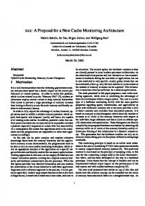
Split Private and Shared L2 Cache Architecture for Snooping-based CMP Xuemei Zhao, Karl Sammut, Fangpo He, Shaowen Qin School of Informatics and Engineering, Flinders University zhao0043, karl.sammut, fangpo.he,
[email protected] Abstract Cache access latency and efficient usage of on-chip capacity are critical factors that affect the performance of the chip multiprocessor (CMP) architecture. In this paper, we propose a SPS2 cache architecture and cache coherence protocol for snooping-based CMP, in which each processor has both private and shared L2 cache to balance latency and capacity. Our protocol is expressed in a new state graph form, through which we prove our protocol by formal verification method. Simulation experiments shows that the SPS2 structure outperforms private L2 and shared L2 structure.
1. Introduction Nearly all existing Chip multiprocessor (CMP) systems use a shared-memory architecture. One of the most important design issues in shared-memory multiprocessors is the implementation of an efficient on-chip cache architecture and associated cache coherence protocol that allows optimal system performance. Some CMP systems employ private L2 caches [1][2] to attain fast average cache access latency by placing data close to the requesting processor. To prevent replication and improve the CMP's performance, IBM Power 4 [3] and Sun Niagara [4] use shared L2 caches to maximize the onchip capacity. Recently, several hybrid L2 organizations have been proposed to reduce access latency through a compromise between the low latency of private L2 and the low off-chip access rate of shared L2. For instance, Adaptive Selective Replication scheme [5], and Cooperative Caching [6] are mainly based on either private L2 or shared L2. These schemes represent significant modifications to the coherence protocol based on standard cache architecture, and are more complex to realize. Furthermore, no formal verification of the modified cache coherence protocols is available. We propose an alternative L2 cache architecture, in which each
processor has Split Private and Shared L2 (SPS2), and the corresponding cache coherence protocol is referred to as the SPS2 protocol. This scheme makes efficient use of on-chip L2 capacity and has low average access latency. Its functional correctness is then proven through formal verification method.
2. Cache Architecture A traditional bus-based shared-memory multiprocessor has either private L1s and private L2s, or private L1s and a shared L2. We refer to these two structures as L2P and L2S, respectively. Both schemes have their advantages and disadvantages. L2P architecture has fast L2 hit latency but can suffer from large amounts of replicated shared data copies which reduce on-chip capacity and increase the off-chip access rate. Conversely, the L2S architecture reduces the off-chip access rates for large shared working datasets by avoiding wasting cache space on replicated copies. In this paper, we propose a new scheme, SPS2, to organize the placement of data. All data items are categorised into one of two classes depending on whether the data is shared or exclusive. Correspondingly, the L2 cache hardware organization of each processor is also divided into two parts, private and shared L2. In this paper, we define a node as an entity comprising a single processor and three caches, private L1 (PL1), private L2 (PL2) and shared L2 (SL2). The proposed scheme places exclusive data in the PL2 and shared data in the SL2 cache. This arrangement provides fast cache accesses for unique data from the PL2. It also allows large amounts of data to be shared between several processors without replication of the data and thus makes better use of the available SL2 cache capacity. The proposed SPS2 cache scheme is shown in Figure 1. SL2 is a multi-banked multi-port cache that could be accessed by all the processors directly over the bus. Data in PL1 and PL2 are exclusive, but PL1 and SL2 could be inclusive. Unlike the unified L2 cache structure, the SPS2 system with its split private
6th IEEE/ACIS International Conference on Computer and Information Science (ICIS 2007) 0-7695-2841-4/07 $25.00 © 2007
and shared L2 caches can be flexibly and individually designed according to demand. First, PL2 could be designed as a direct-mapped cache to provide fast access and low power, while SL2 could be designed as a set-associative cache to reduce conflict. Second, PL2 and SL2 do not have to match each other in size, and they could have different replacement policies. In addition, SPS2 reduces access latency and contention between shared data and private data. It imposes a low L2 hit latency because most of the private data should be found in the local PL2. Shared data will be placed in SL2 which collectively provide high storage capacity to help reduce off-chip access. CPU core
CPU core
CPU core
CPU core
L1I
L1D
L1I
L1D
L1I
L1D
L1I
L1D
PL2
SL2
PL2
SL2
PL2
SL2
PL2
SL2
To Memory
Figure 1. SPS2 cache architecture
3. Description of Coherence Protocol The protocol employed in SPS2 is based on the MOSI (Modified, Owned, Shared, Invalid) protocol and is changed to incorporate six states (M1, M2, O, S1, S2, I). Subscript 1 or 2 indicates whether the block has been accessed by 1 processor or by 2 or more processors. Data contained in PL1 and PL2 may have all six possible states (M1, M2, O, S1, S2, I), while data contained in SL2 has only four states (M2, O, S2, I). The SPS2 protocol uses the write-invalidate policy on write-back caches. To keep consistency and coherency between the three different caches, the cache coherence protocol should also be modified accordingly.
3.1. Coherence Protocol Procedure The protocol behaves as follows. Initially, any data entry in the three caches (PL1, PL2 and SL2) should be Invalid (I). When node i makes a read access for an instruction or data block at a given address, PL1i will be searched first. Since PL1i is empty, then PL2i and SL2 will be searched next. Again, neither PL2i nor SL2 will have the requested data, so a GetS message will be sent on the bus. Since all the caches in all the processors are initially invalid, the memory will put the data on the bus, and PL1i will store the data and change their states from I to S1. If this block is evicted, it will
be put in SL2. If another node j requires this same data shortly after, the data will be copied from SL2 to PL1j without needing to fetch the data from memory, and the state in node i will be changed from S1 to S2. If a read request finds the data in the local PL1i, then no bus transaction is needed and data will be supplied to the processor directly. When node i needs to make a write access and a write miss is detected because the data block is not present in PL1i, PL2i, and SL2, a GetX message will be sent on the bus to fetch data from the other nodes or memory and place the requested data in the recently vacated slot. All the other nodes will check their own PL1 and PL2 caches for the requested data. If none of the other nodes have valid data, then the memory will send data to PL1i and its state will be changed to M1. However, if any node, for example j, finds valid data (M1, M2 or O) with same address as the requested data, the contents will be sent to PL1i and all the caches (including j and excluding i) should invalidate data with the same address. Once the data is placed in PL1i and updated, its state will be changed to M2. Since the SPS2 scheme employs a write-back policy, modified data will not be written back to memory until it is replaced. If the write operation finds the data block in PL1i or PL2i with state M1 or M2 (implying a write hit), then the write hit process will proceed with no bus transactions involved. Suppose that after node i executes a write command, another node j needs to read data from same address. Therefore a GetS message will be placed on the bus requesting the other nodes to send back the data. Node i will check its own PL1i and PL2i , and find the requested data block with state M1 or M2 in PL1i . The modified data will then be placed on the bus and stored in PL1j. The cache state in PL1i will be changed from M1 or M2 to O and that in PL1j will be set to S2. If no free slot is available in any of the caches, then the existing data block will need to be swapped out and replaced with the new block. The old data block in PL1 will be evicted to PL2, if its state is M1 or S1. Data with state S2, M2 or O in PL1 will be relocated to SL2. Data with state M1 evicted from PL2 and data with state M2 or O in SL2 will be returned to memory. If the state of the data in PL1, PL2 and SL2 is S1 or S2, indicating it is shared data, then the data will simply be invalidated.
3.2 State graph of SPS2 cache protocol To maintain data consistency between caches and memory, each node is equipped with a finite-state controller that reacts to the read and write requests. The following section illustrates how the SPS2 protocol works using a state machine description as shown in Figure 2.
6th IEEE/ACIS International Conference on Computer and Information Science (ICIS 2007) 0-7695-2841-4/07 $25.00 © 2007
Each node in the SPS2 architecture has three caches (PL1, PL2, and SL2), each of which has its own state representation. A single vector {XY} represents the state of a single cache block in a node. Since PL1 and PL2 are exclusive, one variable X indicates the state of a PL1or PL2 cache block with six possible states (I, S1, S2, M1, M2, O). Y indicates the state of a SL2 cache block, which has only four states (I, S2, M2, O). Therefore, for each node a cache block could have up to 6×4=24 different states, although some of these states are unreachable. Excluding the set of invalid states, there are only twelve possible states, i.e., II, IS2, IM2, IO, S1I, S2I, S2S2, S2O, M1I, M2I, OI, and OS2. II is the initial state of each data block. Our coherence protocol requires three different sets of commands. All the transition arcs in Figure 2(a) correspond to access commands issued by a local processor. These commands are labelled as read, write. The arcs in Figure 2(b) represent transfer related commands, e.g., replacement commands rep2 (issued when PL2 needs room) and repS (issued when SL2 needs room) and transfer command P_SL2 (data is transferred from PL1 or PL2 to SL2). All the arcs in Figure 2(c) correspond to commands issued by other processors via the snooping bus. They include GetS and GetX. As shown in Figure 2, the cache state of any node will change to the next state according to its current state and the received command.
S2 O
IO
IM2
S 1I
M1I
S 2I
M2I
IS2
S 2S2
read write
II
(a) Commands from processor
S 2O
IO
IM2
S 1I
OS 2
OI
M1I
S 2I
M2I
IS 2
S 2S2
P_SL2 rep2
II
4. Formal Verification of Cache Coherence Protocol Cache coherence is a critical requirement for correct behaviour of a memory system. The goal of a formal protocol verification procedure is to prove that it adheres to a given specification. The cache protocol verification procedure includes checking for data consistency, incomplete protocol specification, and absence of deadlock and livelock. Using formal verification in the early stage of the design process is helpful in finding consistency problems and eliminating them before committing to hardware. In this section, HyTech [7] and DMC [8], two abstraction-level model checkers, are used to verify the SPS2 cache coherence protocol.
OS2
OI
repS
(b) Commands for transfer
S 2O
IO
IM2
S1I
OS2
OI
M1I
S 2I
M2I
IS2
II
S 2S 2
GetS GetX
(c) Commands on bus
Figure 2. State transition graph for the SPS2 cache protocol
The first step is to define the SPS2 protocol using a finite-state machine model. According to [9], we limit ourselves to consider protocols controlling single memory blocks and single cache blocks although the
6th IEEE/ACIS International Conference on Computer and Information Science (ICIS 2007) 0-7695-2841-4/07 $25.00 © 2007
procedure could be easily extended to encompass the whole memory and cache system. Similar with [9], we could use EFSM (extended finite-state machine) to model parameterized cache coherence protocol. The behaviour of the system is modelled as the global machine MG = which is associated with protocol P, where QG ={s1, ..., sn}. si is the possible states of cache blocks in one node. Σ G = ∪ i=1 Σi , F = ,δG: Im(F)×QG× ∑G→QG. We model MG via an EFSM with only one location and n data variables (denoted as x) ranging over the set of positive integers. For simplicity, location could be omitted, hence the EFSM-states are tuples of natural numbers (denoted as c) where ni denotes the number of nodes in states si ∈Q during a run of MG. Transitions are represented via a collection of guarded linear transformations defined over the vector of variables (denoted as x) and (denoted as x'), where xi and xi ' denote the number of nodes in state si , respectively, before and after the occurrence of an event. Transitions have the form G(x) → T(x,x'), where G(x) is the guard and T(x,x') is the transformation. The transformation T(x,x') is defined as x'=M• x+c where M is an n×nmatrix with unit vectors as columns. Since the number of nodes is an invariant of the system, we require the transformation to satisfy the condition x1+...+ xn= x1'+...+xn'. The following gives an informal definition of how the transitions of a cache coherence protocol can be modelled via guarded transformations. Internal action. Caches in a node move from state s1 to state s2: x1'=x1-1, x2'=x2+1with the proviso that x1 ≥ 1 is part of G(x). For example, a read miss makes the state of a node move from IS2 to S2S2. Synchronization. Two nodes synchronize on a signal: a node N1 in state s1 changes to state s2, and another node N2 in state s3 changes to state s4. This is modelled as x1'=x1-1, x2'=x2+1, x3'=x3-1, x4'=x4+1, with the proviso that x1≥1, x3≥1 is part of G(x). For instance, a read miss may not only make a node change from II to S2I, but also make another node change from M1I to OI. Re-allocation. The state of all nodes C1,...,Ck is a constant numberλ of nodes whose state changes to Cz for z>k and to state Ci for i>k: x1'=0,..., xk'=0, xi'=x1+...+xk-λ, xz'=λ. This feature can be used to model bus invalidation signals. If a node has state OI, and the data had been written back to memory, then the state will change from OI to II and, at the same time, all the other nodes need to be changed to II if they have state S1I or S2I. k
Some of the transition rules are listed in Figure 3. Because SPS2 protocol has twelve possible states (II, IS2, IM2, IO, S1I, S2I, S2S2, S2O, M1I, M2I, OI, OS2), we use these twelve variables of integer type to indicate twelve states respectively. In Figure 3, Rule r1 corresponds to a read hit event: If in PL1 or PL2 there exists a valid data with state S1, S2, O, M1, or M2, then the read operation can get data directly with no bus transaction needed. Rules r2 - r7 correspond to read miss events. For the sake of brevity, other events (such as write hit, write miss, replacement, etc.) are omitted in Figure 3. (r1) S1 I+S2I+S2S2+OI+M1I+M2 I+OS2+S2O≥1→__ (r2) II≥1, MkI=0, OI=0 → II'=II-II-1, S1 I'=S1I+1 (r3) II≥1, MkI≥1 → II'=II-1, S2 I'=S2 I+1, MkI'=MkI-1, OI'=OI+1 (r4) II≥1, OI≥1 → II'=II-1, S2 I'=S2 I+1 (r5) IS2≥1 → IS2'=IS2-1, S2S2'=S2S2+1 (r6) IM2≥1 → M2I'=M2I+1, IM2'=IM2-1 (r7) IO≥1 → S2O'=S2O+1, IO'=IO-1
Figure 3. SPS2 protocol description in Hytech
As described before, caches in our SL2 protocol could have six possible states (I, S1, S2, M1, M2, O) for each block. Mk (k=1 or 2) indicates that the cache has the latest and sole copy, so all copies in the other caches should be invalid. The occurrence, for example, of two or more copies of a data block, which are labelled as M and O or S in another node, is inconsistent. Possible sources of data inconsistency are outlined below. (i) MkI >= 1& OS2 >= 1. This indicates that data is inconsistent if a node with state MkI coexists with other cache blocks in other nodes with state OS2. If one node has state MkI, which means this node has exclusive modified data, the no other node should have a valid copy. This is contradicted by another block which is labelled with OS2. In addition, since the state of one node is OS2 then all the corresponding states of the other nodes could only be IS2 or S2S2. Since SL2 is a common shared cache, then the state of SL2 should be coherent. (ii) OS2 >= 2. If more than one node has state OS2 for the same block, then data integrity will not hold, because it is impossible for two or more nodes to own the same block of data. (iii) IS2 >= 1 & S2O >= 1. If one node has state IS2, then SL2 has shared data, and all the other caches should have same state in SL2. However, another node has state S2O, thus implying that SL2 has owned data, which conflicts with the first node state IS2. In order to verify data consistency all possible sources of data inconsistency must first be defined. As
6th IEEE/ACIS International Conference on Computer and Information Science (ICIS 2007) 0-7695-2841-4/07 $25.00 © 2007
proven in [9], whenever both the guards of a given EFSM and the target states are represented via constraints, a symbolic reachability algorithm always terminates. In this way we automatically verify the properties of our SPS2 protocol using the HyTech and DMC tool.
5. Simulation analysis To evaluate the performance, we employ GEMS SLICC (Specification Language Including Cache Coherence) [10] to describe three different cache coherence protocols (L2S, L2P, and SPS2). GEMS is based on Simics [11], a full-system functional simulator. The above three protocols are modified versions of the MOSI SMP broadcast protocol from GEMS. The simulated processor is the UltraSPARCIV which has a 64 byte wide, 64 Kbyte, L1 cache. In L2S, all processors share one 4 MB, 8-way, 4 port SRAM with 18 cycles latency. For L2P, each processor has a private 1 MB, 4-way, 1 port SRAM with 6 cycles latency. In our SPS2, each processor has a private 0.5 MB, 4-way, 1 port SRAM with 5 cycles latency, while at same time four processors share one 2 MB, 8-way, 4 port SRAM with 12 cycles latency. We assume 4GB memory is shared with 200 cycles latency.
metrics: runtime, off-chip-access, and bus-traffic. The results are shown in Figures 3 – 5. The horizontal axis shows 9 benchmarks, as well as the average. The three metrics are normalized with respect to the L2S architecture. As shown in Figure 4, SPS2 undoubtedly needs the smallest runtime and has the best performance among the three architectures. This is because much of the data is kept in the local PL2, which allows fast access. When private data overflows from PL2, it will be transferred to SL2 if SL2 still has available space. The transfer is handled using P_SL2 command. Therefore, SPS2 is much faster because it does not need to make as many off-chip accesses to memory. Data shared by several processors are put in the centrally located SL2 allowing all processors faster access time than the L2S structure. Accesses to SL2 are faster because of its relatively small size and short bus. SPS2 achieve an average 10.6% and 3% reduction in runtimes versus L2S and L2P cache schemes. SPS2 attain better performance for benchmarks LUN, LUC, FFT, RAD, WAN, OCE, and CHO. For benchmark CHO, L2P and SPS2 schemes consume only 37% of the runtime required for L2S. However, for WAS, SPS2 is slower than L2P and L2P, and SPS2 is also slower than L2S for BAR.
TABLE 1. SPLASH2 applications and input parameters
1. 4
Benchmark LU(non-contig.) LU(contig.) FFT radix water(spatial) water(nsquared) ocean(contig.) barnes cholesky
1. 2
Input parameters 512×512 matrix, B=16 512×512 matrix, B=16 256K data points 2M keys 512 molecules 512 molecules 258×258 grid 16384 particles Tk29.O
A set of scientific application benchmarks from the SPLASH-2 suite [12]: radix, FFT, LU, cholesky, ocean, barnes and water are used to evaluate the cache strategies. The PARMACS macros must be installed in order to run these benchmarks. The main parameters of these benchmarks are listed in Table 1. These input parameters enable the applications to run for a long time. To minimise the start-up overhead caused by filling the cache, collection of statistics is delayed after the initialisation period. Since our target applications are specifically focused on supporting large matrix manipulations and mathematical operations as used for control algorithms, we have not simulated commercial benchmarks, like apache, OLTP etc. We have realized and evaluated three different L2 cache architectures, L2P, L2S, and SPS2, and compared their characteristics using three different
L2P
1
L2S SPS2
0. 8 0. 6 0. 4 LUN LUC FFT RAD WAS WAN OCE BAR CHO AVE
Figure 4 Comparison of runtimes for the three architectures
According to Figure 5, for all benchmarks, L2P performs worse than L2S and SPS2 in terms of offchip accesses. Since the L2P scheme suffers from reduced capacity due to the need to store multiple copies of shared data, it will require more accesses to off-chip memory. For BAR, L2P requires 16.5 times more off-chip accesses than L2S. In most benchmarks, the results indicate that, SPS2 imposes only a bit more off-chip accesses than L2S, and certainly much less than L2P. However, benchmarks WAN and BAR work better with SPS2 because they experience less off-chip access, 14% and 5% respectively, than with L2S. On average, SPS2 has only 23% more off-chip access than L2S. The reason is that, in our SPS2, PL2 and SL2 are set-associative and separately located on the silicon die.
6th IEEE/ACIS International Conference on Computer and Information Science (ICIS 2007) 0-7695-2841-4/07 $25.00 © 2007
Consequently it is not always possible to access all of the storage space in either cache. 20 15
L2P L2S
10
SPS2 5
the correctness of the protocol before commencing on the hardware development. By comparing SPS2 with L2P and L2S using critical metrics and relevant benchmarks, it can be seen that SPS2 performs better than the other two cache architectures with respect to runtime and bus traffic. Off-chip accesses for SPS2 are also much less than for L2P, but slightly more than for L2S.
References
0 LUN LUC FFT RAD WAS WAN OCE BAR CHO AVE
Figure 5 Comparison of off-chip access for the three architectures
For shared memory multiprocessor systems, bus traffic reflects the usage of the bus, which increasingly becomes a bottleneck as the number of processors increases. From Figure 6, it can be seen that L2S has the highest bus traffic throughput while L2P consumes less because most private data could be found locally so less bus transactions are needed. Although the SPS2 protocol employs additional operations such as P2_to_SL2, SPS2 still has the lowest bus traffic. 1. 4 1. 2 1
L2P
0. 8
L2S
0. 6
SPS2
0. 4 0. 2 0 LUN LUC FFT RAD WAS WAN OCE BAR CHO AVE
Figure 6 Comparison of bus traffic for the three architectures
6. Conclusion To balance latency and capacity of CMP cache structure, we propose a new cache architecture SPS2 with split private and shared L2 caches. We also propose a corresponding SPS2 cache coherence protocol which is described by means of new state transition graphs in which each node has two states to indicate the states of private L1 or private L2, and shared L2 respectively. Using the state transition graphs, the functional correctness of coherence protocol is proven. The use of formal design verification methods helps identify coherence problems in the early stage, and provide assurance of
[1] K. Krewell, "UltraSPARC IV Mirrors Predecessor". Microprocessor Report, Nov. 2003, pp 1-3. [2] C. McNairy and R. Bhatia. Montecito, "A Dual-core Dual-thread Intalium Processor". IEEE Micro, 2005, 25(2), pp10-20. [3] K. Diefendorff, "Power4 Focuses on Memory Bandwidt". Microprocessor Report. Oct. 1999,13(13), pp1-8,. [4] P. Kongetira, K. Aingaran, and K. Olukotun., " Niagara: A 32-way Multithreaded SPARC processor". IEEE Micro. 2005, 25(2), pp21-29. [5] B. M. Beckmann, M. R. Marty, and D. A. Wood, "Balancing Capacity and Latency in CMP Caches". Univ. of. Wisconsin Computer Sciences Technical Report CS-TR-2006-1554, February 2006. [6] J. Chang and G. S. Sohi, "Cooperative Caching for Chip Multiprocessors". In Proceedings of 33th International Symposium on Computer Architecture, June 2006, pp 264-2765. [7] T. A. Henzinger, P.-H. Ho, and H. Wong-Toi, "HyTech: a Model Checker for Hybrid Systems". In Proceedings of 9th Conf. on Computer Aided Verification (CAV'97), Springer-Verlag, 1997, LNCS 1254, pp460-463. [8] G. Delzanno and A. Podelski, "Model Checking in CLP". In Proc. of TACAS'99, Springer-Verlag, 1999, LNCS 1579, pp 223--239. [9] G. Delzanno, "Automatic Verification of Parameterized Cache Coherence Protocols". 12th International Conference 2000, Chicago, IL, USA, 2000, LNCS 1855, pp53-68. [10] M. M.K. Martin, D. J. Sorin, B. M. Beckmann, et. al., "Multifacet's General Execution-driven Multiprocessor Simulator (GEMS) Toolset", Computer Architecture News (CAN), 2005, 33(4), pp 92-99. [11] P. S. Magnusson et al., Simics: "A Full System Simulation Platform". IEEE Computer, February 2002, 35(2), pp50-58. [12] S. C. Woo, M. Ohara, E. Torrie, et. al., "The SPLASH-2 Programs: Characterization and methodological considerations". In: Proceeding of the 22nd Annual International Symposium on Computer Architecture. Italy, 22-24 Jun 1995, pp24-36.
6th IEEE/ACIS International Conference on Computer and Information Science (ICIS 2007) 0-7695-2841-4/07 $25.00 © 2007