ABSTRACT. The threshold voltage (Vth) of a nanoscale transistor is severely affected by random dopant fluctuations and line-edge roughness. The analysis of ...
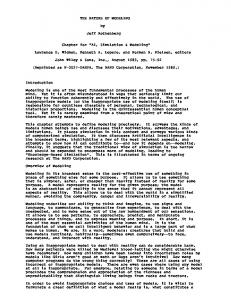
Statistical Modeling and Simulation of Threshold Variation under Dopant Fluctuations and Line-Edge Roughness Yun Ye1, Frank Liu2, Sani Nassif2, Yu Cao1 1
Department of Electrical Engineering, Arizona State University, Tempe, AZ 85287 2
IBM Austin Research Laboratory, Austin, TX 78758
ABSTRACT The threshold voltage (Vth) of a nanoscale transistor is severely affected by random dopant fluctuations and line-edge roughness. The analysis of these effects usually requires atomistic simulations that are too expensive in computation for statistical circuit design. In this work, we develop an efficient SPICE simulation method and statistical transistor model that accurately predict threshold variation as a function of dopant fluctuations and gate length change caused by sub-wavelength lithography and the gate etching process. By understanding the physical principles of atomistic simulations, we (a) identify the appropriate method to divide a non-uniform gate into slices in order to map those fluctuations into the device model; (b) extract the variation of Vth from the strong-inversion region instead of the leakage current, benefiting from the linearity of the saturation current with respect to Vth; and (c) propose a compact model of Vth variation that is scalable with gate size and the amount of dopant and gate length fluctuations. The proposed SPICE simulation method is fully validated against atomistic simulation results. Given the post-lithography gate geometry, this approach correctly models the variation of device output current in all operating regions. Based on the new results, we further project the amount of Vth variation at advanced technology nodes, helping shed light on the challenges of future robust circuit design.
Keywords: Threshold Variation, Random Dopant Fluctuations, Line-Edge Roughness, Non-Rectangular Gate, Atomistic Simulations, SPICE Simulation, Predictive Modeling. 1. INTRODUCTION The aggressive scaling of CMOS technology has inevitably lead to a drastic increase in process variations, such as random dopant fluctuations (RDF) and line-edge roughness (LER) [1][2], Fig. 1 illustrates these variations in the structure of a scaled transistor. These variations interact with each other, profoundly impacting all aspects of circuit performance, especially in the design of SRAM cells which are extremely sensitive to Vth mismatch [3][4]. We traditionally rely on TCAD simulation and compact models to quantify these random variations in circuit analysis, but such methods become incorrect as the minimum feature size of a transistor is approaching the characteristic length of these atom-level effects. Instead, 3D Monte-Carlo atomistic simulations become necessary in order to achieve adequate accuracy. For example, [5] and [6] demonstrated the need for and accuracy of atomistic simulations in the prediction of transistor variations under RDF and LER. However atomistic simulation is not efficient for statistical circuit analysis, such as the optimization of SRAM cells, since it is too computationally expensive to incorporate in traditional circuit analysis and statistical optimization. To alleviate this problem, we need a methodology that enables the compact modeling and SPICE simulation of these random variations with sufficient efficiency, accuracy, and scalability in transistor topology. This modeling and simulation methodology should keep the physicality of atomistic simulation, correctly represent the statistical characteristics, and capture the interaction between RDF and LER in the prediction 45 40 30
th
Line-edge roughness (LER)
σV (mV)
L
Random dopant fluctuations (RDF)
Figure 1. Primary variation sources in a nanoscale device.
With LER: σL = 3nm
35 With LER: σL = 1.5nm
25 20 15 10
Without LER: σL = 0nm
5 100
1000
Transistor Width W (nm) Figure 2. LER increases the variation of Vth, in addition to RDF. Results are predicted from our SPICE simulation method using 65nm PTM [11].
of threshold voltage changes. In this work, we develop such a methodology based on the understanding of the underlying physics, particularly the principles of atomistic simulations and short-channel device physics. RDF is mainly a random effect; but LER is induced by both sub-wavelength lithography and the etching process. Lithography usually has a low spatial frequency and causes the so-called non-rectangular gate (NRG) effect [7][8]. Both RDF and LER change the output current of a transistor by modifying the threshold voltage [9][10]; they further interact with each other, resulting in a significant increase in leakage current [8], and leading to additional Vth variation. Using our newly developed simulation method, we illustrate in Fig. 2 that in addition to the well-known relationship between Vth variation and gate width W [9], LER further exacerbates the deviation of Vth (σVth). Thus increase in the standard deviation of Vth is more pronounced when the transistor width is small, which is the typical condition in SRAM design. To handle these random effects and predict Vth variation from a given gate geometry, we propose to split a non-uniform device into slices, which have an appropriate slice width (d) that is larger than the correlation length of RDF in the leakage region, but small enough to track the spatial frequency of NRG. Each slice is then modeled as a sub-transistor with correct assignment of narrow-width and short-channel effect, as shown in Fig. 3 [8]. Such a representation maps a nonuniform transistor into an array of transistors which can easily be implemented in SPICE. It well captures the statistical characteristics of a transistor under RDF and NRG with sufficient simulation efficiency. Since we choose the slice width to be larger than the atomistic correlation length of RDF, the concept of Vth in a compact device model, which is a statistical average of channel doping, is no longer suitable, particularly in the sub-threshold region [10]. We overcome this problem by extracting Vth from the strong-inversion region. Note that the pronounced velocity saturation effect causes the output current to be a linear function to Vth in the strong-inversion region [11]. Therefore, it provides a correct mathematical basis to partition the channel dopant under RDF, and then linearly superpose them together to monitor the overall change in Vth. Combining this approach with the Equivalent Gate Length (EGL) model that describes the nominal device behavior under non-rectangular gate effect [8], we are able to predict the amount of Vth variation under any given transistor characteristics (e.g., non-rectangular gate, narrow-width effect, etc.). We systematically validate the proposed method with available atomistic simulation results under various conditions, including different amount of LER variations and various transistor sizes. This paper is organized as follows: Section 2 presents the theoretical background from atomistic simulation and device physics, identifying the appropriate slice width and transistor operating region for gate slicing and Vth extraction, respectively. As verified with atomistic simulations, the new SPICE simulation method is shown to accurately predict the variability of saturation current (Ion), leakage (Ioff), and Vth. Based on this method, we further investigate the interaction of RDF, LER, and NRG on Vth variation in Section 3 and show that while the high spatial-frequency component of LER only affects the mean value of Ioff, NRG has a significant impact on both the average and the distribution of the leakage and Vth. We propose a compact model to directly calculate σVth from RDF and LER (Eq. (6)). Finally, we project the trend of Vth variation under RDF and LER toward future technology generations.
2. SIMULATION METHODOLOGY In this section, we present the theoretical background and the flow of the proposed method. The practicality and limitations of gate slicing are well understood from the physical fundamentals. Based on appropriate slice width (d) to split a non-uniform gate, we exploit the linearity of saturation current on Vth change to assign Vth variation due to RDF and LER to each gate slice, and then extract the equivalent threshold variation from the summation of all these slices (Fig. 3). The approach incorporates other effects due to non-uniform gate through the integration of EGL and narrow-width effect models. We comprehensively verify the predicted change of Ion, Ioff, and Vth under various RDF and LER conditions, as compared to 3D atomistic simulation results from [4][5].
2.1 The Fundamentals of Gate Slicing To model a non-rectangular gate in the SPICE environment, a rudimental method is to partition the non-uniform edge into many slices, such that each slice can be approximated into a regular transistor with a uniform gate length. We can then apply the nominal device model 3.5
d
Figure 3. The flow to divide a non-uniform gate into slices. Each slice has a unique Vthi and Li due to RDF and LER.
σL of LER (nm)
3.0
Limited by RDF
Limited by NRG
2.5 2.0
LF LER (NRG)
1.5 1.0 0.5 0.0
HF LER 1
Si data [7] 10
100
Gate Slice Width d (nm)
Figure 4. The appropriate slice width under both effects of RDF and LER [5][7].
to each SPICE for the prediction of I-V characteristics. The final performance of the transistor under NRG is calculated from the summation of currents from all the slices [8][12][13]. This procedure is illustrated in Fig. 3. As long as the current in each slice maintains the direction of source-to-drain, i.e., there is no significant distortion of the electrical field along the channel direction, this method can provide an accurate prediction on the change of I-V under NRG [8][13]. On the other hand, there are two fundamental limitations on the slice width (d) in this approach, especially when we consider the effect of random dopant fluctuations, which requires atomistic simulation to provide sufficient accuracy: 1. Upper bound of d: the spatial frequency of LER. The primary factors to cause LER include sub-wavelength lithography and the etching process. These different factors lead to different spatial frequency and amplitude of the distortion of gate length. Fig. 4 illustrates the silicon data of gate length change under LER [7]. The data clearly shows that two regions of LER have distinct spatial frequency: the high-frequency region (HF) that has a characteristic length smaller than 5nm and a low-frequency one (LF) has a characteristic length larger than 10nm [7]. While the HF component is usually caused by the property of the photo-resist and the etching condition, the LF component is mainly due to sub-wavelength lithography, i.e., NRG, which can be well predicted from layout by lithography tools [8]. The exact values of their characteristic lengths depend on the fabrication technology. When we split a non-uniform gate under LER, the width of each slice needs to be smaller than the characteristic length in order to track the change in gate lengths with adequate accuracy. For instance, to model a typical NRG gate, the slice width should be smaller than 20nm, as shown in the right side of Fig. 4 [7][8]. This phenomenon defines the upper bound of d during the slicing. 2. Lower bound of d: random dopant fluctuations. Due to the random position of dopants in the channel, Vth exhibits an increasing amount of variations with continuous scaling of transistor size [5]. For a relatively long channel device, this behavior is well recorded in the Pelgrom’s model [9]. However, as the channel length is approaching the length scale of the fluctuation, such atom-level randomness can no longer be represented by Vth model in the weak-inversion region, which is usually modeled by averaging the potential in the channel. Such an approach hardly tracks the atomistic change [5]. In order to apply the slicing approach with compact Vth-based device model, the slice width must be larger than the correlation length of random channel potential near the threshold. Such length is typically around several nanometers, depending on the doping concentration [5]. The left side of Fig. 4 shows this lower bound of d during the slicing. If d is smaller than the correlation length, then the partitioning of a NRG gate into many slices is not a correct model for the statistical device behavior under RDF, particularly for the weak-inversion current [5]. Considering these two limits, Fig. 4 illustrates the appropriate region of d where the slicing approach is applicable. Only when d satisfies both limits, the partition of a single NRG transistor is meaningful in physics to prediction the current in all regions. Note that the lower region, which is limited by RDF, usually overlaps with that of the HF component of LER. Therefore, the slicing method may work well for RDF and NRG, but not RDF and HF LER. Since the distribution of gate length under LER approximately follows the Gaussian function [7][8], we use the correlation length of NRG (Wc) as the slice width [14], and follow the normal distribution to generate the length for each slice in the experiments [12][15].
2.2 Saturation Current (Ion)-Based Method A non-rectangular gate shape with σL due to LER and σVth due to RDF
Gate slicing at appropriate slice width 400 140
PTM 65nm
Ion
300
130
250
120
200
110
150
Ioff
100
100
50 90
0 -150
-100
-50
0
50
ΔVth (mv)
100
Ioff (nA)
Ion (μA)
Equivalent Gate Length model for nominal IV characteristics
350
Assignment of Vth to each slice depending on its W, L, and σVth
Extraction of Vth variation from Ion
150
Figure 5. The linear and exponential dependence of Ion and Ioff on Vth change, respectively.
Statistical NRG transistor model by integrating new σVth and EGL models Figure 6. The flow to generate a single device model for statistical analysis of a NRG gate.
After appropriately slicing the gate with a non-rectangular shape, we can describe the characteristic of each slice using compact device model. The summation of all the slices provides the behavior of the original NRG gate. For the nominal condition, each slice has different
Vth from the deterministic effects of narrow-width and DIBL. They lead to the increase in the leakage current and the reduction in the effective gate length. The changes of Ion and Ioff under these effects are well captured through the Equivalent Gate Length (EGL) model [8], i.e., a smaller Lmin for Ioff and a larger Lmax for Ion. In this work, we follow the same modeling approach to formulate the nominal transistor model. However, the situation becomes much more complicated when we incorporate statistical variation due to random dopant fluctuation into each slice. Since the slice width is longer than the correlation length of RDF in the weak-inversion, the concept of Vth is no longer applicable to the leakage current in order to extract Vth variation of the entire NRG transistor [5]. In fact, since Ioff is an exponential function of Vth (Fig. 5), which is very non-linear, the mean and distribution of Vth can not be extracted from the statistical analysis of the summation of Ioff from each slice:
⎛ ⎛ mean of Vth ⎞ Vth ⎞ ⎟⎟ ≠ exp⎜⎜ − ⎟ mean of exp⎜⎜ − n kT q ⎟⎠ ⎝ n kT q ⎠ ⎝
(1)
To overcome this barrier and still maintain the correctness in physics, we leverage the linearity of Ion to study the statistics of Vth. For a short-channel device, Ion has a linear dependence on Vth, due to strong velocity saturation [11]. This behavior is illustrated in Fig. 5 for PTM 65nm technology. This trend becomes even stronger for scaled CMOS devices [11]. As a result, the limitation that fails the statistical Vth extraction from Ioff (Eq. (1)) is removed. The strong linearity of Ion provides a well-behaved basis to study Vth variation under RDF in all cases of NRG. Therefore, we propose to use an Ion-based method to extract Vth variation, embed it into the nominal device model, and then predict Ioff change. Fig. 6 summarizes this flow that supports the development of a single device model for statistical analysis under RDF and NRG. Given the shape of a NRG gate, we first divide it into slices with a suitable width, following the guidance in Fig. 4. Then, the model of EGL is produced for the nominal case under NRG [8]. To investigate the interaction of LER and RDF on Vth variation, we assign Vth to each slice as a statistical variable. While its mean value is determined by the width and length of the slice (i.e., narrow-width and DIBL effect [8]), its standard deviation is also dependent on the size of the slice [6][9][10]:
σV ∝ th
1
(2)
WL
The exact value of σVth due to RDF is technology dependent [2]. From the summation of Ion, we finally extract the variation of the threshold voltage of the entire transistor under NRG and RDF. Since the length of each slice is different under LER, such non-linear relation between σVth and L (Eq. (2)) leads to an increase in Vth variation of the entire transistor, as demonstrated in Fig. 1. The outcome from this procedure is a single device model with EGL and a new σVth, which supports efficient statistical performance analysis for any given NRG and RDF.
2.3 Validation with Atomistic Simulations We implement this method into the SPICE environment and validate its prediction with available 3D Monte-Carlo atomistic simulation results. Fig. 7 compares the prediction of Ion and Ioff variations under random dopant fluctuations [5]. It indicates that under normally distributed RDF, the variation of Ion follows the Gaussian distribution due to its linear dependence on Vth. Meanwhile, the variation of Ioff follows the log-normal distribution because of the exponential dependence of Ioff on Vth. Both mean and sigma of Ion and Ioff are well predicted from the Ion-based extraction method. Fig. 7b further shows that if we directly sum the leakage current from every slice to estimate Vth variation, it results in a significant error, as implied in Eq. (1). 25 20
30 Atomistic simulations SPICE method
25
PDF
PDF
10
15 10
5
16
Mis-prediction from Ioffbased method
20
15
0
Atomistic simulations SPICE method
5
18
20
22
24
26
Ion (μA) (a) Prediction of Ion variation
28
30
0
-10
-9
-8
Log10(Ioff) (b) Prediction of Ioff variation
Figure 7. Validation of Ion and Ioff variations under RDF [5].
-7
-6
Atomistic simulations SPICE method
20
W=50nm
L=30nm
10
th
σV (mV)
15
L=50nm
5 0 0
1
2
3
σL (nm)
Figure 8. Validation of σVth under NRG [5]. In addition to the verification of the Ion-based method under RDF, Fig. 8 evaluates the prediction of σVth under different conditions of gate length variations due to LER, assuming a uniform channel doping concentration (i.e., no RDF) [5]. Two devices are studied, with both gate width at 50nm, and gate length at 30nm and 50nm, respectively. The correlation length of the NRG effect (Wc) is 20nm [5]. For the low-frequency component of LER (NRG), the increase of σL results in a larger amount of threshold variation, due to the interaction between σVth and L, as shown in Eq. (2). This interaction is more pronounced when gate length is shorter, in which case the threshold voltage of each slice is more strongly coupled with L through DIBL effect [8]. As shown in Fig. 8, for a gate with the width of 50nm and the physical length of 30nm, which is typical for a SRAM transistor at the 65nm node, threshold variations can be more than 20mV, purely due to the NRG effect. Meanwhile, the nominal leakage current may increase by more than 15x due to NRG at the same condition [8]. Combining the information together, such effect will be a dominant factor to impact the leakage and circuit stability at the worst case corner. Therefore, it is crucial to incorporate accurate and efficient modeling capability into optimization, in order to mitigate impact of NRG with minimum overhead. Our proposed approach captures this complicated dependence very well, as compared to time-consuming atomistic simulations. It is also ready to be integrated with circuit design tools. While NRG has a pronounced effect on Vth variation, the high-frequency component of LER only has a marginal interaction with Vth variation [5][10]. Since its spatial frequency is quite high, its impact is averaged out across the slice [5]. Instead, it mainly affects the mean value of Ioff, which has been well modeled in the EGL model [8]. Finally Fig. 9 verifies the prediction of threshold variation in the presence of both RDF and NRG. The variation of Vth is evaluated through the distribution of Ioff, which is very sensitive to Vth change due to its exponential dependence. Three sets of experiments are carried out: NRG only with σL at 2nm, RDF with a rectangular gate (i.e., no NRG), and RDF with the NRG shape. Again, gate width is 50nm. Since Vth depends on L through the DIBL effect [8][11]:
⎛ L⎞ (3) Vth = Vth 0 − Vds exp⎜ − ⎟ ⎝ l' ⎠ where Vth0 is a function of channel doping, the change of Vth due to L and RDF can be approximated as: ⎛ L ⎞ ΔL ΔVth = ΔVth 0 + Vds exp⎜ − ⎟ ⋅ ⎝ l' ⎠ l'
(4)
Therefore, the total variation of Vth follows the relationship below, as long as σL and RDF are independent and not excessive: (5)
σ total 2 = σ RDF 2 + σ NRG 2
where σRDF, σNRG, σtotal are Vth variations due to RDF only, NRG only, and the total amount, respectively. The contributions of NRG and RDF are independent to the statistics of Vth. The relationship is well verified with atomistic simulations, as shown in Fig. 9. 0.5
SPICE simulations Model
NRG+RDF
RDF+LER
0.2
RDF only
0.1
LER only (σL =2nm)
20
RDF only
th
0.3
σV (mV)
10 off
(I )
0.4
σlog
30
Atomistic simulations SPICE method
10
NRG only σL =2nm
0.0 20
40
60
80
100
L (nm)
Figure 9. Validation of σVth under both RDF and NRG [4][5].
100
1000
Gate Width W (nm)
Figure 10. Validation of predictive modeling with SPICE results.
Fig. 9 indicates that when L is large, RDF is the dominant factor in threshold variation. As gate length decreases, the importance of NRG rapidly increases in the calculation of Vth variation. Again, the main reason is the strong DIBL effect, which is an exponential function of L, as shown in Eq. 3. Overall, our Ion-based simulation method provides excellent predictions of Vth variation under all situations, as compared to 3D Monte-Carlo atomistic simulations. It significantly enhances the simulation efficiency, with fully compatibility to circuit simulators.
3. PREDICTIVE MODELING Based on the underlying physical mechanisms, we have successfully developed a SPICE simulation method from gate slicing to the extraction of Vth variation in the strong inversion region. In this section, we further propose a compact model that directly predicts Vth variation from RDF and NRG. This model updates traditional Pelgrom’s model with the additional consideration of NRG effect. Using this model, we extrapolate the variation of Vth towards future technology nodes, helping shed light on robust circuit design with scaled CMOS technology.
3.1 Modeling of Threshold Variation For traditional long-channel device, Vth mismatch is mainly induced by random effects, such as the dopant fluctuation. This consideration is the basis for the well known Pelgrom’s model and other Vth variation models, in which σVth is inversely proportional to the square root of the transistor size [2][6][9]. This fact is also shown in Fig. 9, in which the σVth due to RDF is a straight-line in log scale with respect to L. However, as shown in Figs. 1 and 9, the impact of NRG on Vth variation becomes pronounced with further scaling of L, and can no longer be ignored in the calculation of threshold mismatch. These two effects superpose each other in the statistical property of Vth, as shown in Fig. 9 and Eq. (5). As developed in [6][9][10], random dopant fluctuations induce the deviation of Vth as a linear function of (WL)-0.5. For a larger transistor, the random distribution of dopants is averaged out in the modeling of Vth. Akin to this effect, the random distribution of gate length under NRG also leads to a linear function of W-0.5, since the longer gate width is, the more the length distortion is average out. On the other hand, due to the DIBL effect, NRG induced Vth variation has an exponential dependence on L (Eq. (4)). Therefore, we can improve Eq. (5) with the following formula:
σ total 2 =
C1 C2 W 2 + ⋅ c ⋅σ L WL exp(L l ') W
(6)
where Wc is the correlation length of NRG, and C1, C2 and l’ are technology dependent coefficients. The first term describes conventional Pelgrom’s model. The second term is designated to the variation due to NRG. The exponential dependence on L is demonstrated in Fig. 9, with Fig. 10 further verifies Eq. (6) at different gate width. Our model accurately captures the superposition of these two statistical components, as well as the inverse square root dependence on W. As compared to the consideration of both NRF and RDF, traditional RDF only model significantly underestimates the total amount of Vth variation, as shown in Fig. 10. Note that due to the exponential dependence on L of the second term in Eq. (6), the impact of NRG diminishes at long gate length. Yet the second term rapidly affects threshold variation for a device with short gate length and width. For instance, at W=50nm, it has a comparable influence as that of RDF. Therefore, its role can not be neglected, particularly when we design the circuits with minimum size transistors in scaled technologies.
3.2 Projection to Future Technology Nodes After extensive verification with atomistic simulations, the proposed simulation method and compact model offers a solid and convenient tool to explore threshold variation under NRG and RDF effects. As shown in Fig. 9 and 10, such approach has the right sensitivity to the transistor definition, as well as the amount of variations. In this section, we extrapolate these models for future technology generations, with the goal to generate early stage insights to future robust design under increased variations. Continuous scaling exacerbates both RDF and NRG effects. With the scaling of transistor size, the total number of dopants in the channel significant reduces [1]. Consequently, it becomes more challenging to precisely control the position of dopants and as a consequence RDF will be more significant. For line-edge roughness, although the etching process may improve in the future, the situation
Table 1. Projection of threshold variation NRG parameters Wc (nm) 20
50
σVth (mV)
σL (nm)
65nm
45nm
32nm
22nm
0
19.9
23.8
28.1
45.8 71.2
1
21.6
27.8
39.0
2
26.3
39.2
69.4
0
19.9
23.8
28.1
45.8
1
23.8
33.3
51.7
98.6
2
33.3
55.2
105.2
of the low-frequency component, NRG, is not optimistic. Since it is difficult to reduce the wavelength in the photo-lithograph process, the distortion in gate length is expected to increase [12], even though lithography recipes and layout techniques, such as regular layout fabrics, may help improve the situation [12][16]. Using the new Vth variation model (Eq. (6)), we project the amount of threshold variation, under possible scenario of RDF and NRG. The nominal model file is adopted from PTM [11]. Table 1 summarizes the results for various NRG parameters of Wc and σL. Even under the same amount of NRG, the variation of the threshold variations keeps increasing due to the aggressive scaling of the feature size, as well as the increase of short-channel effects. As the trend goes, future design will suffer a dramatic amount of random Vth variation, leading to severe degradation in circuit matching property, memory stability, and the leakage control. While the improvement of process technology will continue, it but may be limited in the future, innovative circuit design and optimization techniques are critical to overcome these barriers.
4. Conclusion Random variation in the threshold voltage is prominent in scaled CMOS technology and can severely affect circuit stability as well as performance distribution. In addition to the well known random dopant fluctuation effect, line-edge roughness, particularly non-rectangular gate, is emerging as a new contributor to Vth variation. Instead of 3D Monte-Carlo atomistic simulations, we propose an efficient simulation method in standard SPICE environment that accurately captures the impact of RDF and NRG on Vth variation. The development of the new method is based on the physical understanding of the atomistic simulations as well as the device physics. In our method, a nonuniform gate is first divided into appropriate slices; then threshold variation is assigned and extracted from the strong-inversion region, with the benefit from the linear dependence of Ion on Vth. The method significantly alleviates the computation cost, provides sufficient fidelity to atomistic simulations and scalability to process and design conditions. Based on this method, we further incorporate the impact of NRG into traditional Pelgrom’s model, identifying the exponential dependence on gate length. With the continuous scaling towards the 22nm node, the effect of RDF and NRG on Vth variations becomes even more critical for future robust design exploration. Our method and compact model provides a physical and efficient tool for statistical circuit performance analysis and optimization.
REFERENCES [1] International Technology Roadmap for Semiconductors, 2006. [2] K. Bernstein et al., “High-performance CMOS variability in the 65-nm regime and beyond,” IBM J. Res. & Dev., vol. 50, no. 4/5, pp. 433-449, Jul./Sep., 2006. [3] Y. Nakagome, M. Horiguchi, T. Kawahara, and K. Itoh, “Review and future prospects of low-power RAM circuits,” IBM J. Res. & Dev., vol. 47, no. 5/6, pp. 525-552, Sep./Nov., 2006. [4] B. Cheng, S. Roy, G. Roy, F. Adamu-Lema, A. Asenov, “Impact of intrinsic parameter fluctuations in decanano MOSFETs on yield and functionality of SRAM cells,” Elsevier Solid-State Electronics, vol. 49, pp. 740-746, 2005. [5] A. Asenov, A. R. Brown, J. H. Davies, S. Kaya, G. Slavcheva, “Simulation of intrinsic parameter fluctuations in decananometer and nanometer-scale MOSFETs,” IEEE TED, vol. 50, no. 9, pp. 1837-1852, Sep. 2003. [6] D. J. Frank, Y. Taur, M. Ieong, and H.-S. P. Wong, “Monte Carlo modeling of threshold variation due to dopant fluctuations,” Symp. VLSI Circuits, pp. 171-172, 1999. [7] J. A. Croon et al., “Line edge roughness: Characterization, modeling and impact on device behavior,” IEDM, pp. 307-310, 2002. [8] R. Singhal, A. Balijepalli, A. Subramaniam, F. Liu, S. Nassif, Y. Cao, “Modeling and analysis of non-rectangular gate for postlithography circuit simulation,” DAC, pp. 823-828, 2007. [9] J. J. M. Pelgrom, A. C. J. Duinmaijer, A. P. G. Welbers, “Matchign properties of MOS transistors,” IEEE JSSC, vol. 24, no. 5, pp. 1433-1440, Oct. 1989. [10] K. Takeuchi, “Channel size dependence of dopant-induced threshold voltage fluctuation,” Symp. VLSI Technology, pp. 72-73, 1998. [11] W. Zhao, Y. Cao, “New generation of predictive technology model for sub-45nm design exploration,” IEEE TED, vol. 53, no. 11, pp. 2816-2823, Nov. 2006. (Available at http://www.eas.asu.edu/~ptm) [12] A. Subramaniam, R. Singal, Y. Cao, “Design rule optimization of regular layout for leakage reduction in nanoscale design,” to be published at ASP-DAC, 2008. [13] P. Gupta, A. Kahng, Y. Kim, S. Shah, D. Sylvester, “Modeling of non-uniform device geometries for post-lithography circuit analysis”, SPIE, vol. 6156, 2006. [14] J. Wu, J. Chen, K. Liu, “Transistor width dependence of LER degradation to CMOS device characteristics,” SISPAD, pp. 95-98, 2002. [15] S.-D. Kim, H. Wada, J. C. S. Woo, “TCAD-based statistical analysis and modeling of gate line-edge roughness effect on nanoscale MOS transistor performance and scaling.” IEEE TSM, vol. 17, no. 2, pp. 192- 200, May, 2004. [16] T. Jhaveri et al., “Maximization of layout printability/manufacturability by extreme layout regularity,” J. Micro/Nanolitho., MEMS and MOEMS, vol. 6, no. 3, 031011, Jul.-Sep. 2007.