efficiently decouple lines with both inductive and capacitive coupling. We generalize the RLC decoupling problem based on transmission line theory and a ...
Switch-Factor Based Loop RLC Modeling for Efficient Timing Analysis Yu Cao1, Xiao-dong Yang2, Xuejue Huang3, Dennis Sylvester4 1
2
3
EECS Department, UC Berkeley, USA; Sun Microsystems, USA; Rambus Inc., USA; 4 EECS Department, Univ. of Michigan, Ann Arbor, USA Therefore, it is desirable to develop a similar methodology that can efficiently reduce a general RLC network into equivalent decoupled RLC nets while capturing the effective loop RLC characteristics. Furthermore, this single line model should be sensitive to both layout structure and the switching pattern of neighboring nets. In particular, the latter issue significantly affects the current return path and leads to large delay uncertainties [6]. In RC line models, such a decoupling can be realized by applying a switch-factor to the coupling capacitance. Depending on the switching behavior of the neighboring nets (i.e., in-phase, out-phase, or quiet), the switch-factor is commonly bounded by (0, 2), or more accurately by (-1, 3) [5, 7]. In this work, we begin by generalizing the switch-factor decoupling approach to a multiple RLC line condition based on transmission line theory, to model the effect of neighbors switching on the loop characteristics. Due to the complexity of inductive coupling and the fact that it leads to opposite-polarity noise as capacitive coupling under the same conditions [1], we show that a Boolean estimation of switch-factor is not applicable in the general RLC case. Considering both inductive and capacitive noise induced by neighbors switching, we propose a more physical methodology to estimate the switchfactor and apply that to solve for loop RLC parameters directly from partial RLC parasitics and the switching pattern. Compared with the previous table-lookup approach for loop RLC modeling [1], this new methodology is more physical and convenient for delay and delay-bound prediction in global routing, clock structure optimization, and other inductance-aware interconnect analysis. This paper is organized as follows. First, the general RLC decoupling methodology is derived from general transmission line analysis in Section 2. Section 3 further presents the calculation of switch-factor in multiple RLC line case. Section 4 applies this new methodology to two design cases: multiple-bit global data-bus and a well-shielded clock structure. Section 5 concludes the proposed modeling approach.
ABSTRACT Timing uncertainty caused by inductive and capacitive coupling is one of the major bottlenecks in timing analysis. In this paper, we propose an effective loop RLC modeling technique to efficiently decouple lines with both inductive and capacitive coupling. We generalize the RLC decoupling problem based on transmission line theory and a switch-factor, which is the voltage ratio between two nets. This switch-factor is also known as the
Miller factor and is widely used to model capacitive coupling. The proposed modeling technique can be directly applied to partial RLC netlists extracted using existing parasitic extraction tools without advance knowledge of the return path. The new model accurately captures the impact of neighboring switching activity when it significantly affects the size of current return loop. As demonstrated in our experiments, the new model accurately predicts both upper and lower delay bounds as a function of neighboring switching patterns. Therefore, this approach can be easily implemented into existing timing analysis flows such as max-timing and min-timing analysis. Finally, we apply the new modeling approach to a range of activities across the design process including timing optimization, static timing analysis, high frequency clock design, and data-bus wire planning.
Keywords RLC model, loop inductance, switch-factor, current return loop, static timing analysis, slew rate, data-bus, and clock.
1. INTRODUCTION With high switching frequencies, fast signal transition time and low resistivity copper technology in modern VLSI designs, on-chip interconnects often exhibit transmission line behavior. For long global wires, a distributed RLC model must be used for correct performance analysis, particularly in high-speed global buses and the clock distribution network. Due to the slow decay of inductive coupling with increasing line spacing and the uncertainty of the current return loop in onchip interconnect structures, the full L matrix must be extracted in contrast to capacitance extraction that only considers the nearest neighbors [1]. The sparsity of a modified nodal analysis (MNA) matrix is therefore lost due to the dense partial inductance matrix, causing computational effort to increase tremendously. In the past ten years, many researchers have attempted to reduce the analysis complexity such as local truncation or the use of a K or susceptance matrix [2-4]. However, there is no technique that is simple, practical, efficient, and accurate for timing analysis, where couplings are the major bottleneck in the runtime of the analysis process. The switch-factor (or Miller factor) is a simple and widely-used method to decouple nets in the capacitive domain and efficiently identify either max- or min-timing violations [5]. Permission to make digital or hard copies of all or part of this work for personal or classroom use is granted without fee provided that copies are not made or distributed for profit or commercial advantage and that copies bear this notice and the full citation on the first page. To copy otherwise, to republish, to post on servers or to redistribute to lists, requires prior specific permission and/or a fee. ICCAD’03, November 11-13, 2003, San Jose, California, USA. Copyright 2003 ACM 1-58113-762-1/03/0011 ...$5.00.
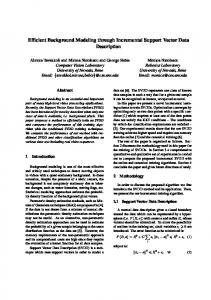
2. TRANSMISSION LINE ANALYSIS Fig. 1 illustrates the layout configurations of multiple parallel lines in a global metallization layer. The lines in the underlying orthogonal layer only contribute to metal-to-ground capacitance, but not inductance. After the line dimensions are defined (Fig. 1a and b), partial RLC parasitics can be extracted using either field solvers (e.g., RaphaelTM) or closed-form analytical models [8, 9]. For each line, the driver is modeled as a linear resistor (i.e., Thevenin model) and loading capacitance is added at the far-end of the line. In the case of power and ground lines that are often inserted among signal lines as shield wires, the ends are shorted to ground (Fig. 1b). The goal in this work is to decouple the target line from others and create an equivalent single line model for efficient and accurate timing analysis (Fig. 1c). Definitions of line parameters are given in Table 1.
848
w
s
TABLE I. LINE PARAMETER DEFINITIONS
Full RLC Parameters per Unit Length*
t h
(a) Power/Ground Target Line
cli length
Vink
rdri
rdrk
rloop
lloop
r
and
0 0
0
rj
0
0
L L L L v C = 0 − cci ,i −1 0 0 0 0
r
mutual inductance between ith and jth lines
cgi
ith line-to-ground capacitance
ccij
coupling capacitance between ith and jth lines
rdri
ith line linear driver resistance
cli
ith line loading capacitance
tr
input signal rise time
trout
output signal rise time
0 L , 0 v L = L L 0 L O
0 L
rloopi
ith line loop resistance
lloopi
ith line loop inductance
cloopi
ith line loop ground capacitance switch-factor between ith and jth lines ( =Vi/Vj )
V V c gi + 1 − i −1 cci −1,i + 1 − i +1 cci+1,i Vi Vi Vi ∂2 ⋅ + 2 ∑ l sk + lmki V ∂t i V V c gk + 1 − k −1 cck −1,k + 1 − k +1 cck +1,k k V V k k Vk +1 Vk −1 cck +1,k Vk cck −1,k + 1 − ⋅ c gk + 1 − Vk Vk
L
L
Lsi
Lmij
Lmji L
Lsj L
0 0
c gi + cci ,i −1 + cci ,i +1 L
− cci ,i +1 L
0
L
(2)
Therefore, if we define:
where R , L , and C are the resistance, inductance, and v capacitance matrices, respectively; V is the voltage vector. They are defined as: 0 ri
lmij
V V ∂ 2Vk ∂ = rk c gk + 1 − k −1 cck −1,k + 1 − k +1 cck +1,k Vk Vk Vk ∂x 2 ∂t
Since the line is represented by distributed RLC segments, general transmission line theory is applicable to describe the switching behavior. The voltage equation of multiple RLC lines is expressed by the following: v v v v v ∂V v v ∂ 2V ∂ 2V (1) + LC = RC ∂t 2 ∂t ∂x 2
M O v Vi , v 0 V = R= V 0 j M 0
ith line self inductance
*Corresponding capital letters represent total values, assuming all lines have equal length; for the target line, i = k;
Figure 1. Multiple line configurations and loop RLC model. (a) Cross-sectional view of line dimensions (b) Multiple line structure (c) Equivalent single line model for target line
v
lsi
Sij
ctk
cloop
(c)
v
ith line resistance
Loop RLC Model Parameters per Unit Length*
(b)
Vink
ri
Switch-factor S ij =
L , L L L
Vi Vj
rloopk = rk
(3) (4)
c loopk = c gk + (1 − S k −1, k ) c c ( k −1), k + (1 − S k +1, k ) c ck , ( k +1) (5)
c lloopk = lsk + ∑ loopi ⋅ Sik ⋅ lmik i cloopk
0 0 . 0 L L
(6)
then the differential equation for Vk (Eqn. (2)) can be converted to:
∂ 2V k ∂ ∂2 (l loopk c loopk )V k (7) = ( r c ) V + loopk loopk k ∂x 2 ∂t ∂t 2 Considering Eqn. (7) captures exactly the same response of a single RLC line (with loop rlc) to input voltage Vk, we conclude that the transformations in Eqns. (3-5) provide an equivalent loop RLC model for the target line. The above solution for loop RLC provides a physical means of decoupling RLC lines: the loop RLC has line resistance unchanged; loop capacitance (Cloop) is computed using the same concept as the switch-factor in RC decoupling. Note that if all ls and lm equal to 0, the line condition is reduced to RC and the
Note that for C , since capacitive coupling decays very quickly as space increases, only the nearest neighbors need to be considered. v For L , all elements must be included because inductive coupling is a long-range effect. For the target line (i = k as in Table 1), the corresponding equation for Vk can be expressed based on Eqn. (1):
849
and C should be the total loop values). Note that for a line with pronounced inductive effects, trin/2