Invited Talk, 3rd Asia Pacific Conference on HDL (APCHDL-96), Jan 8-10, Bangalore, India.
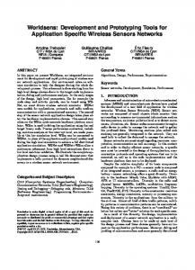
Synthesis for Prototyping of Application Specific Processors Adam Postula*, David Abramson, Paul Logothetis† Abstract This paper presents our experience with the development of Application Specific Processors (ASP) for simulation and optimization problems. The focus is on the design methodology that allows rapid development of application specific processors. As a design case we describe and analyse the design process applied to the development of a specialised processor for simulation of sintering in metallurgical research. 1. Introduction Application Specific Processors [1], [2], [3], [4], [5] had been around for years before a general computer became enough powerful to tackle complex computational problems. Differential equation solvers used in tracking systems are excellent examples of highly specialised computing machines, not necessarily digital. Those machines could perform like supercomputers (at that time) for the application they were tailored to. Unfortunately they were very costly to build and finally got replaced by more flexible and cheaper general sequential computers. Despite the power of modern computers many computational tasks in science and engineering are so time consuming that the concept of a specialised co-processor for solving a problem or a class of problems is still attractive. The recent surge in Field Programmable Gate Array technology [10],[11] made it possible to think of application specific architectures that can be reprogrammed for different kind of problems. This way the performance of application tailored hardware can be complemented with the flexibility of a programmable solution. Supercomputer-like performance can be achieved at a fraction of cost, at least in theory. Fig. 1 below shows an Application Specific Processor (hardware accelerator) connected to the host computer. host computer
ASP reprogrammable accelerator
Program development
Accelerator compilation
ACCELERATOR CODE
Accelerator down-loading
Accelerator execution
Quick process, done every time the program is executed
Slow process, done once while preparing the program
Fig 1. Basic configuration of a computer system with reprogrammable accelerator
There are a number of issues that must be solved before this approach can gain wide acceptance. We concentrate in this presentation on the design methodology that allows rapid development of application specific processors. * Department
of Electrical and Computer Engineering, University of Queensland, St. Lucia Campus, Brisbane, Australia. email:
[email protected] † Faculty of Science and Technology, School of Computer and Information Technology, Griffith University, Brisbane, Australia, email:
[email protected], email:
[email protected]
1
2. Development methodology An application specific processor system as depicted in Fig. 1 should not impose additional requirements on the operator when using programs that have been developed to run on the ASP. Loading a program and executing it can be as easy as on a general purpose computer. Unfortunately, programming such architectures is not simple. Software expertise must be complemented with detailed knowledge of hardware design to efficiently implement algorithms in hardware. In general, the development process is a hardware/software co-design and it can result in more hardware design than software development, depending on the algorithm to be implemented. It is essential to use hardware design tools that allow team members with different level of hardware design knowledge to easily communicate and understand the design requirements. Simulation and synthesis tools based on hardware description languages such as VHDL are best suited for this purpose[7], [8]. As our project focuses on the development of ASP for optimization algorithms we do not experience all the problems typical in hardware/software co-design. Fig 2 below presents the ASP design flow based on simulation and synthesis that we apply. algorithm specification
sequential implementation
partitioning
software module
hardware module simulation synthesis
profiling and refinement verification implementation
Fig 2. Design flow in the development of Application Specific Processors for optimization problems
The essential process in our design flow is the careful profiling of an algorithm that is usually available as a sequential implementation. This profiling gives us information that can be used to improve the sequential implementation and more importantly to make architectural decisions in the hardware development. Once the algorithm is optimised as the sequential implementation partitioning into the software and hardware components is considered. We strive to implement as much as possible in hardware since this gives the best speed-up. The software module is usually limited to providing a user interface and to maintaining larger data structures on the mass storage devices of the host processor. Development of hardware is done in a typical VHDL simulation and synthesis environment. The Mentor Graphics Design Architect is used for VHDL simulation and synthesis, NeoCAD tools are used for mapping the design onto XILINX FPGAs. An APTIX system is used to provide programmable connectivity between FPGAs [12]. Our hardware prototyping platform is made of an APTIX board supporting up to 4 programmable interconnection matrices (FPICs) and 16 XILINX 4010 FPGAs. Custom designed static
2
memory modules can be inserted into the sockets of FPGAs providing the necessary off-chip memory. 3. The Design Case The ASP implementation of the sintering simulation algorithm is a very interesting design case since it illustrates many of the architectural decisions based on the analysis of the sequential algorithm. Sintering is the metallurgical process in which an object is formed by heating a metal powder to a temperature below its melting point [9]. The simulation of sintering is very important for better prediction of the sintering results and control of process parameters. Simulation on the atomic level provides the best insight into the mechanisms of sintering but is computationaly very costly. A highly optimised sequential algorithm presented in Fig 3, implemented in Fortran and executed on Sparc 5 required about 3 days of CPU time to complete the simulation.. WHILE not finished DO read address of hole choose random neighbour read hole and neighbour IF neighbour is atom THEN retrieve neighbours of hole retrieve neighbours of atom calculate deltaN // difference in number of atoms calculate value of probability function P(deltaN) choose random number R(0-1) IF R < P THEN write swapped hole and atom update hole address END IF END IF increment hole array counter END WHILE Fig 3. The Pseudo-code of the sintering simulation algorithm
As it can be seen from the code above the algorithm is of Monte Carlo type. The simulated system is a very much scaled down version of the real sintering of three copper wires. The total number of elements - atoms and holes is about 2 million. The characteristic feature of the problem is a very small fraction of elements (holes) that are moved at one Monte Carlo step. The data representation is very simple and consists only of three bits for each element. Operations on data are also very simple and restricted to comparisons and simple additions. The most complicated operation in the sequential algorithm seems to be the generation of random numbers. Profiling the simulation runs provided invaluable information used in making the architectural trade-offs. The results of the profile showed that the ratio of movable holes to all the holes processed in the simulation was about 0.02 and the ratio of holes that actually moved to all the processed holes was 0.0016. Clearly the implementation should be optimised to check the holes as quickly as possible while moving a hole can take much more time without noticeable degradation of simulation performance.
3
We investigated two different architectural options for a sequential implementation. The first was a very simple “scanning” architecture in which all the elements of the system were checked for possibility of movement. A nice feature of this architecture was the ease of parallelisation of hole movement computations. However since the number of moveable elements (holes) is very small, the scanning architecture proved to be too slow, even when parallelised. The second “holes only” architecture shown in Fig 4a stems directly from the optimised sequential algorithm as presented in Fig.3.. HOLE ARRAY
BANK 1
UPDATE HOLE & TAG
BANK 2
do not move
COUNTER BANK 0
READ HOLE ADDR
NEXT HOLE INDEX
ADDRESS GENERATOR
...
GEN ADDRESS
ne
ig
ou
r=
move
RANDOM NUMBER
hb
ho
le
MAIN MEMORY
READ HOLE & NEIGHB
CALCULATE MOVE
REGISTERS
neighbour = atom READ HOLE & NEIGHBs
READ ATOM NEIGHBs
CALCULATE MOVE READ ATOM NEIGHBs
(b)
(a) read hole address choose random neighbour generate address increment counter choose random move read hole & neighbour read hole neighbours read atom neighbours read atom neighbours decide / calculate move write atom & neighbour cycle
1
2
3
4
5
6
7
8
9
10
11
(c) % of processed holes
100%
0.5 - 50%
0.25 - 2%
Fig 4. Architecture (a), state diagram (b) and timing (c) of “holes only” sintering processor The hole array memory is small as the number of holes is only about 1% of atoms. A simple counter increments the array index to the next hole to be processed. The random number generator rand is a module running autonomously and delivering a random number twice in processing each cell. The address generator calculates addresses of cells to be fetched from the cell memory. Since there are three memory banks the address generator must produce nonconsecutive addresses and that makes its logic complicated. The main cell memory stores the whole map of elements and is organised as three way interleaved memory banks. A set of registers regs is used to hold the data fetched from the memory and keep it stable during computation of the move which is done by the calculate move module. As it is seen from the timing diagram in Fig 4c checking each hole for movability is done in
4
4 cycles. Moving a hole is done in the subsequent 7 cycles but this happens only for a small fraction of holes. The simulation performance would be much increased if checking could be done in a shorter time. This has been achieved by pipelining the architecture. Pipelining increased the time necessary to move a hole but dramatically decreased the checking time to just one cycle. Another trade-off which was required was in computation of the sintering process parameters - rugosity and porosity. These parameters can be computed on a host computer as their values are needed only every several thousand regular Monte Carlo steps. This requires dumping the ASP memory to the host processor. On the other hand to compute porosity a number of holes in the system can be counted by simply incrementing the porosity counter whenever a properly tagged hole is read from the main memory. A rugosity counter can be incremented whenever the hole tagged as having an atomic neighbour is found. Thus, the computation of the process parameters in the ASP imposes very little additional hardware and results in decreased communication with the host computer. Simulation and synthesis from VHDL descriptions has been used throughout the design process. Since the AutoLogic synthesis system does not allow behavioural synthesis the design has been partitioned into blocks matching those in Fig. 4 and simulated and synthesised on the RTL level. The final mapping to FPGAs and APTIX is under way. Table 2 summarises the estimated performance of the two architectures for both FPGA and gate array technology. Table 1: Technology
Architecture
Cycle Time
Total Cycles
MCS/sec
Speedup
SS5
Fortran - holes only
--
--
57
1.0
Xilinx 4010
Scanning - pipelined
50 ns
4.69 x 10¹¹ 85
1.5
Holes only
100 ns
1.96 x 10¹⁰ 1183
20.8
Holes only - pipelined
100 ns
6.12 x 10⁹
3268
57.3
Scanning - pipelined
30 ns
4.69 x 10¹¹ 142
2.5
Holes only
50 ns
1.96 x 10¹⁰ 2040
35.8
Holes only - pipelined
50 ns
6.12 x 10⁹
Gate Array
6536
114.7
The cycle times are technology and architecture dependent. For the “holes only” architectures, address generation is the most time consuming operation, since it involves a table look-up and three parallel 20-bit additions. Hence the cycle time is determined by the speed of the address generator. For the scanning architectures the address generator is a simple counter. Table 1 assumes that the chosen memory has a cycle time which is not longer than the machine cycle time. 4. Conclusions and further work We have discussed the use of simulation and synthesis in the design of Application Specific Processors for acceleration of optimization and simulation problems. The design case presented in detail proves that very substantial speed-ups can be achieved in a fairly simple architectures for some classes of problems. There is an open question if High Level Synthesis can be successfully applied to automatic generation of FPGA based ASPs with computational performance 5
better than general purpose computers. As demonstrated in this paper, the RTL level synthesis of a pipelined architecture and rather careful design of the memory system has resulted in the estimated speed-up of about 50 times.Further work will focus on applying behavioural synthesis to the sintering and other algorithms and trying to achieve speed-ups comparable to those reported in Table 1. If successful, this can pave the way for automatic program compilation for ASP architectures. 5. Acknowledgments The authors would like to acknowledge the contribution of our colleagues at the University of Queensland, namely Professor Kevin Burrage, Dr. Graham Schaffer and Dr. Ivan Podolsky. This project is supported by the Australian Research Council References: 1. R.W. Hartenstein, Custom Computing Machines, Copernicus CP 94:0536 BenefitDMM’95 2. R.W. Hartenstein, J.Becker, R.Kress,H.Reinig,K.Schmidt, A Two-level Hardware/ Software Co-design Framework for Automatic Accelerator Generation, Copernicus CP94:0536 Benefit-DMM’95 3. Abramson, D.A., "A Very High Speed Architecture to Support Simulated Annealing ", IEEE Computer, May 1992. 4. D. Abramson, "High Performance Application Specific Architectures", Proceedings of 26th Hawaii International Conference on System Sciences, Kauai, Hawaii, Jan 1993. 5. R.Razdan, M.D.Smith, A High-Performance Microarchitecture with Hardware-Programmable Functional Units, MICRO-27 -11/94 San Jose, USA. 6. R.Venkateswaran, P.Mazumder, Coprocessor Design for Multilayer Surface-Mounted PCB Routing, IEEE Trans. on VLSI, Vol.1, No.1, March 1993. 7. Axel Jantsch, Peeter Ellervee, Johnny Öberg, and Ahmed Hemani, “A Case Study on Hardware/Software Partitioning”, Proceedings of IEEE Workshop on FPGAs for Custom Computing Machines, Napa, CA, April 1994. 8. Axel Jantsch, Peeter Ellervee, Johnny Öberg, Ahmed Hemani, and Hannu Tenhunen, “Hardware-Software Partitioning and Minimizing Memory Interface Traffic”, Proceedings of EURO-DAC ‘94, Grenoble, France, September 1994. 9. T. Sercombe, “A Monte Carlo Simulation of Sintered Microstructures”, Bachelor of Engineering Thesis, Department of Mining and Metallurgical Engineering, The University of Queensland, 1994. 10. D. Bursky, Advanced 100-kgate FPGA Family Takes On Gate Arrays, Electronic Design, May1, 1995. 11. D.Bursky, FPGA Routing Enhancements Boost the Usability Of Complex Logic, Electronic Design, May1, 1995. 12. XILINX and APTIX data books
6