APPLIED PHYSICS LETTERS
VOLUME 83, NUMBER 15
13 OCTOBER 2003
Terahertz imaging with nanometer resolution Hou-Tong Chen and Roland Kerstinga) Department of Physics, Rensselaer Polytechnic Institute, Troy, New York 12180
Gyu Cheon Cho IMRA America, 1044 Woodridge Avenue, Ann Arbor, Michigan 48105
共Received 28 May 2003; accepted 15 August 2003兲 We report on the application of scanning near-field optical microscopy for terahertz imaging. We demonstrate a spatial resolution of 150 nm for 2.0 THz pulses. Our experiments show the feasibility of submicron THz microscopy for imaging of biologic tissues on the cell level or for the investigation of individual submicron semiconductor devices. © 2003 American Institute of Physics. 关DOI: 10.1063/1.1616668兴
The first demonstrations of terahertz 共THz兲 imaging have stimulated many suggestions for applications, ranging from biomedical imaging to the inspection of semiconductor devices.1,2 It soon became clear that for many applications a microscopic resolution would be required. Biomedical THz imaging of the inner cell will demand submicron resolution since the cell itself can be smaller than 10 m. Similarly, the inspection of individual semiconductor devices would require nanometer spatial resolution. Such resolution has been out of range for a long time since Rayleigh’s criterion restricts resolutions in far-field microscopy to the wavelength’s scale, which can be several hundred micrometers for THz radiation. Far-field imaging techniques with resolutions close to the diffraction limit have been demonstrated on biological tissues and semiconductors.1,3 However, subwavelength resolutions require near-field techniques. Resolutions down to 7 m were achieved using metallic subwavelength apertures4,5 or optically gated apertures.6,7 Further improvements are mostly restricted by the strong signal attenuation due to the apertures, which leads to a decrease of the field strength with the third power of the aperture’s diameter.8 An alternative concept can be adapted from scanning near-field optical microscopy 共SNOM兲 and was recently demonstrated for the mid-infrared9 and the microwave regions,10 where resolutions as small as 10⫺6 were achieved. In these works, the resolving aperture was substituted with a sharp tip and scattering of the incident radiation was measured. In this letter, we describe the application of this apertureless SNOM technique for THz imaging. We achieved a spatial resolution of 150 nm. Few-cycle THz pulses were generated by femtosecond laser excitation of n-doped InAs with 70 fs laser pulses of 780 nm wavelength and 8 nJ pulse energy. Their center frequency is 2.0 THz, which corresponds to a wavelength of 150 m. A more detailed description of the spectroscopic configuration, as well as typical THz pulse shapes, can be found in Refs. 11 and 12. As shown in Fig. 1, the THz pulses are focused onto the structure under investigation to a spot size of about 500 m. The angle of incidence is 70° and the electric field is p-polarized. Spatial resolution is achieved by a sharp metallic tip, which is placed above the structure. The a兲
Electronic mail:
[email protected]
incident THz pulses induce a dipole moment in the tip– surface system, leading to scattering and absorption of part of the THz radiation. The remaining transmitted signal is detected either by electro-optic sampling13 or by a 4 K bolometer. Electro-optic sampling allows us to map the electric field of the reflected THz pulse in time-domain with a bandwidth of 2.5 THz. Alternatively, we used for detection the bolometer, which has a bandwidth of 10 THz. However, in this case, only the power of the transmitted radiation can be detected. In order to determine the spatial resolution, we fabricated metallic stripes on semi-insulating silicon. These gold structures have periodicities between 10 and 40 m and a thickness of 2 m. The spacings between the metallic lines are nonconductive, which leads to transmission properties as described in Ref. 11. Images of the stripes were recorded by moving the structures with respect to needle and the focus of the THz pulses. In our SNOM technique, the spatial resolution is achieved by the dipole moment that is induced by the THz radiation in the tip and in the underneath region below the sample surface. The most commonly used model for the tip– surface polarizability approximates the imaging tip as a sphere of radius R, which has a distance z to the surface. In this model, the polarizability of the tip and the effective po-
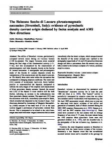
FIG. 1. Schematic of the experimental technique. The THz beam is focused to the diffraction limit onto the surface of the sample. Part of the incident radiation is scattered and absorbed by the tip-surface system. The transmitted THz radiation is detected either by electro-optic sampling or with a bolometer.
0003-6951/2003/83(15)/3009/3/$20.00 3009 © 2003 American Institute of Physics Downloaded 27 Oct 2003 to 131.215.237.113. Redistribution subject to AIP license or copyright, see http://ojps.aip.org/aplo/aplcr.jsp
3010
Appl. Phys. Lett., Vol. 83, No. 15, 13 October 2003
Chen, Kersting, and Cho
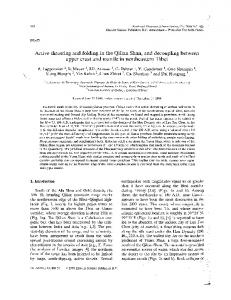
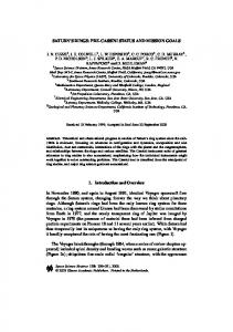
FIG. 2. Line scan across metallic stripes, which have a spacing of 10 m. The profile is reproduced by THz electro-optic imaging. FIG. 3. Terahertz image of semi-insulating silicon with metallic stripes of nominally 10 m width.
larizability of the tip–surface system are given by:9,14
␣ tip⫽4 R 3
⑀ t ⫺1 , ⑀ t ⫹2
␣ eff⫽
␣ tip关 1⫹ 共 ⑀ s ⫺1 兲 / 共 ⑀ s ⫹1 兲兴 1⫺
␣ tip 关共 ⑀ s ⫺1 兲 / ⑀ s ⫹1 兲 ] 16 共 R⫹z 兲
,
3
共1兲
where ⑀ t and ⑀ s are the dielectric constants of the tip and of the surface, respectively. Applying Mie theory leads to scattering and absorption cross sections of C sca⫽
83 3
4
兩 ␣ eff兩 2 ,
C abs⫽
2 Im兵 ␣ eff其 .
共2兲
As pointed out in Ref. 14, the absorption cross section exceeds the scattering cross section by orders of magnitude. Furthermore, the scattering efficiency strongly depends on the radius of the tip used. We expect a dependence on R 3 for the reduction of the THz field strength due to absorption and scattering using material parameters of the tip–surface system for 2.0 THz.15 Even more important is that the scattering efficiencies are extremely small. Using a tip radius of R⫽1 m, we calculated relative changes of the THz field, which are smaller than 10⫺4 . Figure 2 shows a THz line scan across metallic stripes with a nominal linewidth of 10 m. The data were recorded using the electro-optic sampling technique and a tungsten needle with 1 m tip radius. For reference, we first recorded the profile of the gold lines by measuring a small probecurrent through the tungsten tip in contact mode 共upper part of Fig. 2兲. During the following THz measurement the tip is held at a constant height of about 200 nm above the sample. The lower part of the figure shows that the periodic profile is reproduced by the THz measurements. The amplitude of the modulation signal was 0.25 nA, which corresponds to 0.2% of the incident THz signal. Higher signal intensities of up to 0.6% can be achieved when scanning closer to the surface. We deduced spatial resolutions 共10% to 90%兲 as small as 4 m, of which a significant part results from the tip radius of 1 m. Measurements of the scattered signal were performed in time-domain for tip positions above the gold lines and between them. Except for a difference in the overall ampli-
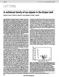
tude, no significant dispersive differences were observed. This is reasonable because neither gold nor silicon have strong dielectric features in the spectral range covered by our THz pulses. We therefore limit the following discussion to the spatial resolution, which can be achieved with the scanning-tip method. Figure 3 shows a two-dimensional scanning image of metallic stripes having a width of 10 m. The data were recorded by electro-optic sampling of the THz pulse. The image consists of 60⫻20 data points and was measured with an integration time-constant of 300 ms. This allows for an acquisition time of less than 10 min. The metallic stripes can be clearly resolved. The deduced resolution is 3 m, which corresponds to about /50. In fact, submicron resolutions can be achieved with smaller tip sizes. Figure 4 shows a line scan across the edge of a grating line, which was recorded with a tip of about 100 nm radius. The upper part illustrates the profile of the step
FIG. 4. Line scan across the edge of a stripe. A 10% to 90% resolution of 150 nm was achieved. Downloaded 27 Oct 2003 to 131.215.237.113. Redistribution subject to AIP license or copyright, see http://ojps.aip.org/aplo/aplcr.jsp
Appl. Phys. Lett., Vol. 83, No. 15, 13 October 2003
and the lower part shows the detected THz signal. The profile of the step as given by the current through the needle is reproduced by the THz data with a 10% to 90% resolution of 150 nm. Again the signal intensity is about 0.4% of the incident THz signal. We observed a similar relative signal intensity of about 0.3% in experiments where a bolometer was used for time-integrated detection. Remarkably, we did not observe a reduction of the signal intensity by a factor of 10⫺3 when reducing the tip size from 1 m to 100 nm, as it would be expected for a spherical scatterer. Furthermore, we achieved signal intensities of about 0.5%, either for the modulated field amplitude or for the power of the modulated THz signal,16 which exceed the theoretical values by two orders of magnitude. These results indicate that the model of a spherical scatterer needs to be refined.14 In fact, the scatterer does not only consist of the spherical tip, but also of the upper part of the needle, which has antenna-like properties that lead to a highly confined field below the tip.17,18 Our preliminary model calculations have shown field enhancements of up to three orders of magnitude and a field energy below the needle, that is nearly independent on the tip diameter. These findings may explain the strong signal intensities that we observed, which will be discussed in a forthcoming work. The implication of our experimental findings is that even higher spatial resolutions can be realized by using nanometer-sized tips without suffering extreme signal losses. In conclusion, we have demonstrated the application of scanning near-field microscopy techniques for THz imaging. A spatial resolution of 150 nm has been achieved, which corresponds to about /1000. These submicron resolutions may allow THz imaging of the interior of biologic cells.
Chen, Kersting, and Cho
3011
Other applications may arise in the field of submicron semiconductor device inspection and far-infrared quantum optics on individual quantum dots. This research was supported by an award from Research Corporation and by Semiconductor Research Corporation. The authors thank I. Wilke and X.-C. Zhang for stimulating discussions and S. Kraatz for technical assistance. B. B. Hu and M. C. Nuss, Opt. Lett. 20, 1716 共1995兲. See Reviews in Sensing with Terahertz Radiation, edited by D. Mittelman 共Springer, Berlin, 2002兲. 3 P. Y. Han, G. C. Cho, and X.-C. Zhang, Opt. Lett. 25, 242 共2000兲. 4 S. Hunsche, M. Koch, I. Brener, and M. C. Nuss, Opt. Commun. 150, 22 共1998兲. 5 O. Mitrofanov, M. Lee, J. W. P. Hsu, I. Brener, R. Harel, J. F. Federici, J. D. Wynn, L. N. Pfeifer, and K. W. West, IEEE J. Sel. Top. Quantum Electron. 7, 600 共2001兲. 6 Q. Chen, Z. Jiang, G. X. Xu, and X.-C. Zhang, Opt. Lett. 25, 1122 共2000兲. 7 N. C. J. van der Valk and P. C. M. Planken, Appl. Phys. Lett. 81, 1558 共2002兲. 8 H. A. Bethe, Phys. Rev. 66, 163 共1944兲. 9 B. Knoll and F. Keilmann, Nature 共London兲 399, 134 共1999兲. 10 B. Knoll, F. Keilmann, A. Kramer, and R. Guckenberger, Appl. Phys. Lett. 70, 2667 共1997兲. 11 A. Filin, M. Stowe, and R. Kersting, Opt. Lett. 26, 2008 共2001兲. 12 R. Ascazubi, O. C. Akin, T. Zaman, R. Kersting, and G. Strasser, Appl. Phys. Lett. 81, 4344 共2002兲. 13 Q. Wu, M. Litz, and X.-C. Zhang, Appl. Phys. Lett. 68, 2924 共1996兲. 14 B. Knoll and F. Keilmann, Opt. Commun. 182, 321 共2000兲. 15 F. Zenhausern, Y. Martin, and H. K. Wickramasinghe, Science 269, 1083 共1995兲. 16 The relative modulation signals for field and power detection differ only by a factor of two because of the small scattering efficiencies. 17 J. R. H. Cory, A. C. Boccara, and A. Lahrech, Microwave Opt. Technol. Lett. 18, 120 共1998兲. 18 A. Bouhelier, M. Beversluis, A. Hartschuh, and L. Novotny, Phys. Rev. Lett. 90, 013903 共2003兲. 1 2
Downloaded 27 Oct 2003 to 131.215.237.113. Redistribution subject to AIP license or copyright, see http://ojps.aip.org/aplo/aplcr.jsp