236
IEEE TRANSACTIONS ON VERY LARGE SCALE INTEGRATION (VLSI) SYSTEMS, VOL. 20, NO. 2, FEBRUARY 2012
Testable Path Selection and Grouping for Faster Than At-Speed Testing Xiang Fu, Huawei Li, Senior Member, IEEE, and Xiaowei Li, Senior Member, IEEE
Abstract—Faster than at-speed testing provides an efficient way for testing of small delay defects (SDDs). It requires test patterns to be delicately classified into groups according to the delay of sensitized paths. Each group of patterns is managed to be applied at certain frequency. In this paper, we propose to generate tests for faster than at-speed testing based on path delay fault (PDF) model and single path sensitization criterion. An effective testable path selection and grouping method is introduced, which could quickly and accurately identify paths whose delay falls into a given delay span. Several techniques are used to improve the efficiency of the testable path selection procedure. Experimental results on ISCAS’89 benchmark circuits show that the proposed method could achieve high transition fault coverage and high test quality of SDDs with low CPU time. Index Terms—Faster than at-speed testing, small delay defects (SDDs), testable path selection.
I. INTRODUCTION S the dimension size of devices continues to shrink, the performance of devices becomes more and more vulnerable to delay variations. Process variation, crosstalk, power supply noise, and resistive opens and shorts cause plenty of small delay variations [1]. For the delay uncertainty caused by process variation, crosstalk and power supply noise, increasing the design margin will help relieve the problem. But the resistive shorts and opens in interconnects and vias not only increase the propagation delay but also impact the reliability and lifetime of fabricated chips. For example, a resistive open defect at a metal wire may become real open because of the electronic migration effect, and result in permanent damage to the chip. As a result, this kind of defects, which is also called as small delay defects (SDDs), should be effectively tested if high reliability is the first consideration [2]. To achieve the best test quality of SDDs, a transition should be justified and propagated along a longest path through each fault site during test generation. It is well known that the tendency of sensitizing short paths in transition fault (TF) test generation fail to detect SDDs. The current research works on SDD testing are mainly based on the TF model and have tried to involve timing
A
Manuscript received January 14, 2010; revised June 21, 2010; accepted November 23, 2010. Date of publication January 13, 2011; date of current version January 18, 2012. This paper was supported in part by the National Natural Science Foundation of China under Grant 60776031, Grant 60633060, and Grant 60921002 and in part by the National Basic Research Program of China (973) under Grant 2011CB302501 and Grant 2011CB302503. The authors are with the Key Laboratory of Computer System and Architecture, Institute of Computing Technology, Chinese Academy of Sciences, Beijing 100190, China (e-mail:
[email protected];
[email protected];
[email protected]). Digital Object Identifier 10.1109/TVLSI.2010.2099243
information in TF test generation to solve the above problem [3]–[7]. However, the runtime of timing-aware automatic test pattern generation (ATPG) may be 20 times higher than that of a traditional ATPG [8]. Furthermore, due to poor testability of longest paths, it is nearly impossible for ATPG procedures to find a longest testable path set to cover all the fault sites. In [8], a test pattern selection scheme for SDD testing is proposed. The patterns are selected from the existing N-detect patterns of transition faults. Pattern selection techniques can be applicable and efficient, but the test quality depends on the original N-detect test set. Another promising approach for detecting SDDs is faster than at-speed testing [9]–[12]. By increasing the test clock frequency, the SDDs will be more likely to be detected, since higher frequency will lower the slack of the target fault site. Faster than at-speed delay testing can be applied to the circuit under test (CUT) using two categories of methods. The first one controls the on-chip phase-locked loop (PLL) [13] to generate high-speed clock pulses. Such a technique is widely used in modern chips and is supported by many commercial tools. However, the maximum frequency is constrained by the PLL used in the chip. The cost of changing frequency is also high, because the PLL needs a great deal of time to sample the reference clock. The second method uses an on-chip programmable capture generator (PCG) [14] to generate system clock-independent high-frequency capture cycles with low hardware overhead. The configure information for the PCG can be embedded in test patterns and supports the three main test frameworks, that is, launch on shift (LOS), launch on capture (LOC), and enhanced scan (ES). Test pattern grouping is an important issue in faster than at-speed testing. Existing techniques mainly focus on reducing the delay variations of the selected pattern set [9], [10]. A delay test might sensitize multiple paths. Test frequency could be determined by the delay of the longest sensitized path [9], [10], or by the delay of a shorter sensitized path under test (PUT) [11]. In the first situation, the test could only guarantee the test quality of the fault sites on the longest sensitized path and the sensitized paths which have slacks close to that of the longest sensitized path. From this point of view, it is better to use a path oriented fault model in faster than at-speed testing. In the second situation, the output flip-flop of longer sensitized paths must be masked to avoid false timing failure. Scan flip-flop masking is highly undesirable in delay testing, and should be effectively avoided [12]. The method proposed in [12] also considered the power supply noise effect. In this paper, we propose a testable path selection and grouping method for faster than at-speed testing based on the
1063-8210/$26.00 © 2011 IEEE
FU et al.: TESTABLE PATH SELECTION AND GROUPING FOR FASTER THAN AT-SPEED TESTING
path delay fault (PDF) model and single path sensitization criterion. It deterministically and efficiently targets paths with lengths belonging to (or close to) a given path length span and lets shorter paths have higher priority to be selected. Several techniques are presented to reduce the CPU time of the testable path selection procedure. The proposed method has the following contributions. 1) Using the PDF model, tests can be generated targeting the available test frequencies and grouped according to the delay of the PUTs. Instead of struggling on the poor testability of long paths, we now have the choice of selecting paths which have shorter delay and perhaps better testability to cover timing edges (or TFs). Furthermore, shorter paths are less susceptible to random process variations than longer paths are, and they could detect smaller defect size in the presence of process variation [2]. Since faster than at-speed testing makes the shorter PUT timing critical, the required test quality of SDDs can be guaranteed. 2) By using the single path sensitization criterion, the generated test patterns can be applied with less scan flip-flop masking, and the test results are guaranteed without causing test invalid problems in delay testing. These patterns also have less switching activities, and hence are easier to be used to control power dissipation under high test frequencies. Finally, quantitative metrics, which are derived from the statistical delay quality model (SDQM), are proposed to evaluate the test quality of the generated tests, as well as possible overtesting under faster than at-speed testing. Experimental results show that the proposed method could achieve high TF coverage and high test quality of SDDs with low CPU time. The remainder of this paper is organized as follows. In Section II, the motivation of this paper is explained. In Section III, we present a method to find paths whose delay falls into the given path length span. In Section IV, we describe the proposed path selection and grouping method. Test quality evaluation methods for faster than at-speed testing is introduced in Section V. Experimental results on ISCAS’89 benchmark circuits are shown in Section VI. Finally, we conclude the work in Section VII. II. MOTIVATION Here, the path sensitization criteria and the corresponding path testability are discussed first. Then, a case study on benchmark circuit S38584 is made to reveal the relations between testability and path length. Finally, we discuss false positive and false negative problems in faster than at-speed testing. A. Path Sensitization Criteria for Path Delay Test A delay test consists of two vectors, . The first vector V1 initializes the circuit to a stable state, while the second vector V2 launches a transition and propagates it through a path to an output so that the targeted delay defect could be detected. A path is referred to a combinational path that starts from a primary input (PI) or the output of a flip-flop (called pseudoprimary input, or PPI), and ends at a primary output (PO) or the input of a flip-flop (called pseudoprimary output, or PPO). For
237
each combinational path in a circuit, there are two PDFs corresponding to rising and falling transitions on the start (or end) point of the path. Gates that are on the PUT are called on-path gates. Lines that are on the PUT are called on-inputs. Lines that are not on the PUT but are inputs of the on-path gates are called side-inputs. In order to generate a test for a PDF, each side-input of each on-path gates should be assigned to appropriate noncontrolling value according to side-input constraints in the path sensitization criterion. A multi-input gate has two kinds of noncontrolling values: a static noncontrolling value and a to-non. There are mainly four controlling transition under classes of path sensitization criteria employed in path delay test generation: single path sensitization, robust test, nonrobust test, and functional sensitization [15]. Among them, robust and nonrobust sensitization criteria are most commonly used in ATPG. A two-vector test is a robust path delay test if it guarantees the detection of the target path delay fault regardless of the delays at all other circuit lines. Path sensitization criterion of robust test generation is as follows [16]. 1) To propagate a to-controlling transition at an on-input of should imply a static nonconan on-path gate, trolling value at each side input of the gate. 2) To propagate a to-noncontrolling transition at an on-input of an on-path gate, only V2 should imply a noncontrolling value at each side-input of the gate. In other words, should imply either a static noncontrolling value or a to-noncontrolling transition at each side-input of the gate. Nonrobust sensitization criterion only requires V2 to imply a noncontrolling value at each side-input of an on-path gate, no matter what kind of transition is propagated through the gate. It is looser than the robust criterion, but it can’t guarantee to detect the delay defect of the PUT if there are other delay defects in the circuit. Functional sensitization criterion is even looser than nonrobust sensitization criterion, and is not cared about in this paper. to The single path sensitization criterion requires imply a static noncontrolling value at each side-input when either of the transitions is propagated through an on-path gate. It is tighter than the robust sensitization criterion, while only one transition can be propagated to the output of the PUT. A single-path sensitization test can guarantee, if a delay fault is detected, the delay defect is exactly on the PUT, but a robust test cannot. Obviously, the tighter the path sensitization criterion is, the harder the test is to be found. Previous research works showed that, a large percentage of the paths in benchmark circuits are robustly untestable, or even nonrobustly untestable, not to mention single-path sensitizable. B. Testability Analysis on Path Length Critical path selection is important for delay testing considering SDDs. Since a path may have poor testability that no test can be generated to propagate a transition along the path, testability is a must consideration in path selection. Delay test generation is to find a two-vector test that sensitizes a path, satisfying the constraints of all the side-inputs of the on-path gates. Apparently, the larger the number of on-path gates (also called
238
IEEE TRANSACTIONS ON VERY LARGE SCALE INTEGRATION (VLSI) SYSTEMS, VOL. 20, NO. 2, FEBRUARY 2012
Fig. 2. A test example for transition fault model.
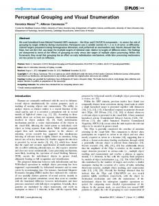
Fig. 1. Testable PDFs and testable PDF ratio of S38584.
gate level of the path) is, the harder the path is to be sensitized. A case study on benchmark circuit S38584 is made to reveal this phenomenon. In S38584, there are 1 080 723 combinational paths, and the corresponding PDF number is 2 161 446. We enumerate the millions of the PDFs. For each PDF, its path length is recorded first. Then an ATPG procedure is called to justify whether it is testable. Here path length is the sum of on-path gate delays, while interconnect delay is ignored. Note that, the propagation delay of rising transition and falling transition (i.e., logic timing edges) for a gate are different, but we don’t take this difference into account for simplicity. The max delay of the circuit is evenly partitioned into 20 path length spans. Paths whose delay falls into the same span are grouped together. For each group, we record the number of total PDFs and the number of testable PDFs. In this experiment, both nonrobust and robust path sensitization criterion are utilized. The testable PDF number and the total PDF number of each group are shown Fig. 1(a). The testable PDF ratio, which is the ratio of the testable PDF number to the total PDF number of each path length group, is shown in Fig. 1(b). As we can see, for the short paths (group 1–5), over 80% of the total PDFs are testable. As the path delay gets larger, the testable PDF ratio decreases sharply (group 6–9). The testable path ratio remains a stable low level (under 20%) for the long paths (group 10–20). S38584 is a circuit with a high maximum gate level. Long paths of such circuits have poor testability. Note even when interconnect delay dominates the circuit delay, it is reasonable that paths with larger delay tend to have higher gate level, thus lower testability. As a result, it will be fruitless to look for testable paths from the long path set. Selecting testable paths among the shorter paths is a possible solution.
For each testable path, the logic timing edges on this path are called covered by its test. If a logic timing edge is not on any of the testable paths, it is regarded as uncovered. The logic timing edge coverage is then the ratio of number of the covered edges by the testable paths to the total number of logic timing edges in the CUT. For S38584, the logic timing edge coverages of all the nonrobust testable paths and robust testable paths can then be obtained as 95.18% and 90.28% respectively. It should be noted that, for robust and single path sensitization test patterns, if a logic timing edge can be covered by a testable path, the corresponding TF of the logic timing edge can also be covered. But it is not true for nonrobust test patterns. Since a nonrobust test pattern needn’t control the value of the first vector V1 in a delay test, the test pattern may be invalid for a TF on the path under test, which is also figured out in [17]. As we can see, using tighter path sensitization criterion in path delay testing won’t lower the logic timing edge coverage too much. So it is expected that even if single path sensitization criterion is utilized, it won’t cause too much logic timing edge coverage lose either. In the later parts of this paper, we attempt to use the PDF test generation and single path sensitization criterion to achieve good TF coverage. The experimental result meets this expectation well. The reason why single path sensitization criterion is selected in this work instead of robust or other path sensitization criteria, will be discussed in the next subsection. C. False Positive/Negative in Faster Than At-Speed Testing In faster than at-speed testing, both false positive and false negative can occur in the test results. Test power will also become more serious than that in at-speed testing. In this subsection, we will show that, if fault models and fault sensitization criteria are not properly considered, undesirable problems will be occurred during faster than at-speed testing. The most commonly used delay testing fault models are TF model and PDF model. Due to the limited number of faults and high fault coverage, TF model gains much more favor than PDF model. For a TF, the ATPG procedures are likely to propagate the fault effect at the fault site to multiple PO/PPOs in order to increase the chance of finding a test. As a result, a TF test may sensitize multiple paths, as shown in Fig. 2. In faster than at-speed testing, the test clock cycle for the test in Fig. 2 could be determined by the delay of the longer sensitized path ( in Fig. 2). In this situation, though the slow-to-rise TFs on the shorter path could be covered by this test pattern, the test quality of the TFs on the shorter path can’t be guaranteed. The test clock cycle also could be determined by the delay of the shorter sensitized path ( in Fig. 2). In
FU et al.: TESTABLE PATH SELECTION AND GROUPING FOR FASTER THAN AT-SPEED TESTING
Fig. 3. A test example of a robust testable PDF.
this situation, the test clock will sample the value in the static hazard area of the longer path, and the corresponding scan flip-flop should be masked to avoid false positive (i.e., the test mistakenly indicates a timing failure). Such masking will cause lose of fault coverage and/or increase of pattern count, which are undesirable. As a result, only the TFs on the shorter path could be covered by the test. Since TF tests have to be analyzed to get the sensitized paths for a proper test frequency, PDF could be a more straightforward fault model to be targeted in faster than at-speeding testing. Therefore, we adopt PDF model, and expect that the generated tests could be grouped according to the delay of the PUTs. Considering the cumulative delay of a path, it is natural for a PDF test to detect SDDs if a long path is targeted for test generation. In faster than at-speed testing, the target paths needn’t to be long paths, but paths with small slacks in particular faster than at-speed test frequencies. Hence, short paths with high testability could be considered to improve fault coverage. Using short paths as PUTs causes new test invalid problems. For robust PDF sensitization criterion, if a short path is the PUT, the generated test may also be a robust test for a longer path which shares the same PI/PPI and PO/PPO with the PUT. For example, the test in Fig. 3 is a robust test for PUT FF2-G1-G5-G4-FF6. At the mean time, the generated test is also a robust test for PDF FF2-G1-G2-G3-G4-FF6. Since the two sensitized path share the same PPO, it won’t involve scan flip-flop masking problems. However, because of the longer delay of PDF FF2-G1-G2-G3-G4-FF6, this test, if applied in a fast test frequency according to the length of the PUT FF2-G1-G5-G4-FF6 ( in Fig. 3), may always fail and report SDDs detected even there is no SDD on the short path. Obviously, such false positive problems will cause yield loss. For single path sensitization, only one path is sensitized for the targeted PI/PPI and PO/PPO pair of the PUT. So this problem will not appear when using single path sensitization. For nonrobust test patterns, it is well known that test invalidity can occur due to delay faults on side paths. The situation of test invalidity becomes extremely worse if short paths are the target paths. Fig. 4 is an example of an invalid nonrobust test. Suppose the PUT is FF2-G1-G5-G4-FF6. If there are large size of TF faults both on the PUT and on the side path G2-G3, the falling transition at the on-path input of gate G4 arrives no later than the rising transition at the side-input, the output of G4 will be static ’0’, resulting the mask of both fault effects. This is a typical test quality problem that may result in false negative. Single path sensitization criterion will also overcome the false negative problems. Since the side-inputs of on-paths gate need to be assigned to static noncontrolling values, only one path is
239
Fig. 4. A test example of nonrobust test failure.
tested, and the longest sensitized path for the sampled PO/PPO is the very PUT. So there are no other paths sensitized to the same PO/PPO to invalid the test. Scan flip-flop masking should be used to avoid false positive when the transitions on the on-inputs and the side-inputs are propagated through longer paths whose delay exceeds the test clock cycle. Since single-path sensitization criterion requires the side-inputs to be assigned to static noncontrolling values, it will cause the least false positive problems in comparison with TF model and PDF model using other path sensitization criteria. During ATPG, constraints could be introduced to prevent the transitions on the on-inputs from propagating through longer paths whose delay exceeds the test clock cycle. In this way, scan flip-flop masking problems can be avoided. On the other side, the test patterns generated by single path sensitization criterion will cause less switching activities. As a result, the test power, which is a serious problem in faster than at-speed testing, is less than TF model and PDF model using other path sensitization criteria. However, very low switching activities may result in under-testing. In this case, pattern merge and X-filling methods can be introduced to adjust the switching activities to a proper level. Based on the above analysis, we adopt PDF model and single-path sensitization criterion for faster than at-speed testing and try to achieve high SDD detecting quality by selecting and grouping shorter testable paths. To deal with the numerous path-delay faults, a testable path-selection algorithm which is linear to the complexity of the CUT is proposed. The patterns for PDFs can be easily grouped for faster than at-speed testing because single-path sensitization criterion is utilized. High TF coverage could be achieved by the shorter paths which have higher testability, so that faster than at-speed testing for selected shorter paths can gain good test quality of SDDs. III. FINDING PATHS WITH CERTAIN DELAY Here, an efficient path-selection method is introduced, which could find out a set of paths to cover the timing edges as many as possible. The proposed method adopts block-based static timing analysis (STA), and the efficiency of block-based STA is inherited. Using the static timing information, paths belong to (or close to) certain length spans could be effectively targeted. For a given timing edge (arc), the latest arrival time, minimum required time, earliest arrival time, and maximum required time (Definitions 1–4) of the edge can be calculated by one pass forward traverse and one pass back traverse of the whole circuit. Definition 1: The signal latest arrival time of an edge is defined as the longest subpath delay starting from any PI(PPI) to . the edge (excluding the edge), and denoted as
240
IEEE TRANSACTIONS ON VERY LARGE SCALE INTEGRATION (VLSI) SYSTEMS, VOL. 20, NO. 2, FEBRUARY 2012
Fig. 5. Slack analysis of a timing edge.
Definition 2: The signal minimum required time of an edge is defined as the longest path delay of the whole circuit minus the longest subpath delay starting from the edge (including the . edge) to any PO(PPO), and denoted as Definition 3: The signal earliest arrival time of an edge is defined as the shortest delay starting from any PI(PPI) to the . edge (excluding the edge), and denoted as Definition 4: The signal maximum required time of an edge is defined as the longest path delay of the whole circuit minus the shortest delay starting from the edge (including the edge) to . any PO(PPO), and denoted as The slack of the longest path through the edge, which is also the minimum slack of all paths through the edge (denoted as ), and the slack of the shortest path through the edge, which is also the maximum slack of all paths through the edge (denoted as ) can be calculated, respectively, by
(1) (2) The slack of each path through the edge belongs to a span form to . For a certain edge, to select paths belong to a certain path group whose delay falls into a given length span, is equal to select paths whose slack falls into a given slack threshold span. is given, three If a slack threshold span conditions should be considered to search a path whose slack belongs to (or close to) the slack threshold span as illustrated in Fig. 5. In condition 1, of the edge is smaller than , which means all paths through this edge are longer paths against the slack threshold span. In condition 2, is larger than , which means all paths through this edge are shorter paths. In condition 3, the slack span of the edge has an overlap with the slack threshold span, shown in black. Only through edges satisfying condition 3, does there exist paths whose delay falls into the target path length span implied by the slack threshold span. As we know, a PDF is constructed by a series of TFs. To construct a PDF, firstly an uncovered TF whose timing information
Fig. 6. Process of path growing. (a) The ith slack threshold span. (b) The new path stem (NS) after a fan-in edge is chosen. (c) Slack span of NS after a fan-in edge is chosen.
satisfies condition 3 is treated as a seed in the proposed path selection method. A path stem grows up from the seed TF by selecting edges from its fan-in edges and fan-out edges. If a fan-in edge is chosen, the chosen fan-in edge is called head of the new path stem. If a fan-out edge is chosen, the chosen fan-out edge is called tail of the new path stem. The timing information of chosen edges also needs to satisfy condition 3. Similarly, we can and of a path stem, which are the minget imum slack and the maximum slack of all the paths which conand of a path stem tain the path stem. The . constitute its slack span, denoted as There are several types of timing edges (arcs) in block-based STA, for example, inverting sense (NOR, NAND, NOT), noninverting sense (OR, AND, BUFF), nonunate sense (XOR, XNOR) and tri-state enable. In the process of path growing, the transition direction also has to change according to the type of chosen timing edge. If a nonunate sense (or tri-state) gate is encountered, the transition direction is determined by the value assigned to the side-input (or enable port) of the gate. During ATPG, the side-input (or enable port) of a nonunate sense (or tri-state) gate on the PUT should be assigned to a static value to sensitize the PUT. In order to achieve high TF coverage with a minimum testable PDF set, it is better to choose an uncovered TF whose transition direction is consistent to the current transition direction. The process of path growing is illustrated in Fig. 6. As shown in Fig. 6(a), the maximum delay of the circuit (de) is divided into even spans. is set to 20 for noted as demonstration. Thus, the ith path-length span is . These spans are transferred to slack threshold spans
FU et al.: TESTABLE PATH SELECTION AND GROUPING FOR FASTER THAN AT-SPEED TESTING
241
to which the selected paths ought to belong. In the process of path growing, the slack span of the current path stem , is initially as(denoted as CS), signed as the slack span of the seed TF. The slack span of selected subpath is narrowed down as the path stem grows up. After a fanin edge is chosen, it becomes the head of the new path stem (denoted as NS), as shown in Fig. 6(b). The value of NS is decreased by , and the value is increased by , as shown in Fig. 6(c). Hence, the slack span of . and NS becomes can be calculated by (3) (4) where
is the delay of the chosen fan-in edge , and are the signal earand liest and latest arrival time of , are the signal earliest and latest arrival time of the head edge of CS. is chosen and becomes the tail of When a fan-out edge value of NS is decreased by , and the NS, the value is increased by . Hence, the slack span of . and NS becomes can be calculated by (5) (6) where is the delay of the tail edge of CS, and are the signal maximum and minimum required and are the signal maxtime of , imum and minimum required time of the tail edge of CS. During the phase of path growing, if an edge with multiple fan-ins (or fan-outs) is encountered, the path-selection procedure needs to judge which fan-in (or fan-out) edge should be selected. In the judgment procedure, a greedy strategy is and be the slack deviation of CS (as shown adopted. Let in Fig. 6(c)), which are calculated by (7) (8) If is larger than , it’s reasonable to choose an edge with from the fan-in (or fan-out) candidate edges. The the largest chosen candidate edge has to satisfy a constraint (9) In constraint (9), is the value of NS. As a result, constraint (9) guarantees the slack span of NS still has an overlap with the given slack threshold span. However, there may be no fan-in (or fan-out) edge that satisfies constraint (9). The slacks of all paths through the edge are a series of discrete values. Even the slack span of the path stem overlap with the given slack threshold span, there may be no path through the edge with a slack falling into the given slack threshold span. As a result, it is inevitable for the path-selection
Fig. 7. Proposed testable PDF selection flow.
procedure to select paths which have a slack out of the given slack threshold span. In this situation, the selected path is discarded for simplicity. is smaller than , it’s reasonable to choose a candidate If from the fan-in (or fan-out) edges. The edge with the largest chosen candidate edge has to satisfy a constraint (10) This fan-in edge and fan-out edge-selection mechanism will and . The competition will set up a competition between make the slack of the final selected path belong to (or be close to) the slack threshold span. IV. PATH SELECTION AND GROPING STRATEGIES A. Testable Path-Selection Flow After a path with certain length is identified, a combinational ATPG procedure is performed to justify whether the path is testable. The proposed testable PDF selection flow is displayed in Fig. 7. In the proposed flow, the slack threshold spans are used to guide the path-selection procedure in an arranged order according to the path-selection strategy discussed later in Section IV-C. The objective is to find testable paths to cover all of the TFs, with slacks as small as possible under faster than at-speed test frequencies. Since an identified PDF with certain length might be untestable, it is reasonable to attempt multiple times for one seed TF to produce PDFs in order to increase the chance of finding a testable PDF. In the proposed method, each uncovered TF is used as a seed TF for no more than times. The value of is a quantitative measurement of the effort spent in -th slack threshold span. If paths have already been attempted and none of them is testable, the next uncovered TF is selected as a seed. If a testable PDF is found, all on-path TFs are marked as covered since we use single sensitization criterion. The path-selection procedure stops when all of the slack
242
IEEE TRANSACTIONS ON VERY LARGE SCALE INTEGRATION (VLSI) SYSTEMS, VOL. 20, NO. 2, FEBRUARY 2012
threshold spans are processed or all of the TFs are covered by selected testable paths. A bitmap which traces the exercised paths is established during ATPG. The size of the bitmap is the number of the PDFs in the circuit. A PDF is said to be exercised when it is justified to be testable or proved to be untestable. As we know, a PDF is justified to be untestable so long as a subpath of the PDF is justified to be untestable. The information of the untestable subpath can be utilized. Since the subpath is untestable, any PDF that contains the subpath can be proved to be untestable, and the corresponding bit in the bitmap can be set as exercised. Since the PDFs, which share the same subpath, have consecutive path identifiers, the bitmap is always a sparse matrix. So optimization can be made to reduce memory cost. This strategy could reduce the number of calls of the ATPG procedure significantly. Testable paths selected for the same slack threshold span will be tested at the same test frequency associated with the span. A simple pattern merge procedure is developed to merge the patterns which will be applied at the same frequency. It sorts these patterns first in the descending order of the number of X-bits in each pattern. Every time a new pattern is generated, a pattern merge procedure is called traversing the ordered pattern list to justify whether the new pattern is consistent with the existing patterns in the list. If it is consistent with one of the existing pattern, merge the two patterns into a new pattern (while the old existing pattern is deleted), and then insert the merged pattern into the ordered pattern list according to the number of X-bits in it. B. Test Frequency Determination and Path Grouping In faster than at-speed testing, the test frequency of each pattern is constrained by two factors. The first one is the maximum and possible frequencies that can be used in faster than at-speed testing. The second one is the delay of the sensitized paths. Since PDF model and single path sensitization criterion is adopted in this paper, we expect the testable paths to be grouped according to the delay of PUTs. One can first decide the set of different test frequencies to be used in path grouping based on the maximum and possible frequencies that could be obtained. As has mentioned, an on-chip PLL or an on-chip PCG could provide such test frequencies to reduce test cost of using an external ATE. The possibility of providing a number of faster than at-speed capture clock cycles using on-chip PCG has been proved in both [14] and [18]. In [18], an on-chip PCG was proposed to generate high test frequency with low hardware cost. It uses two buffer chains to control the interval between the launch and capture clock edges, and demonstrates the minimum cycle of the generated test clock could be 15.45 ps, which is the delay of a buffer in a 0.18- m technology library. Next, based on available test frequencies, the slack threshold spans can be determined and then used for path selection. Suppose a customer application could provide test frequencies, and the test clock of the xth frequency is calculated by (11)
Fig. 8. Relationship between test period and the slack threshold spans.
TABLE I
k VALUE OF THE iTH SLACK THRESHOLD SPAN
is the clock period of at-speed testing, which can where be determined by the delay of the longest path in the CUT. As described above, after the path-selection procedure is performed, groups of testable paths with slack values belonging to the corresponding slack threshold spans are obtained. A slack threshold spans simple grouping strategy is to get . In the proposed method, is set to directly, i.e., times of m, i.e., . Every slack threshold spans are grouped into a test frequency group. Paths belonging to slack threshold spans of the same test frequency group are tested at one test frequency. As illustrated in Fig. 8, the th (from left to right) slack threshold in the slack threshold spans (denoted as slack threshold period_x), is the span of the total slack threshold spans. C. Path-Selection Strategy The value configured to each slack threshold span will influence the efficiency of the proposed method. For the long paths which have poor testability, most of them are untestable. As a result, most of the effort spent in mining testable paths from the long paths may be in vain. Based on this analysis, it is better to spend less effort on the long paths (corresponding to slack threshold spans with large in Fig. 8) and more effort on the short paths (corresponding to slack threshold spans with small in Fig. 8). On the other hand, in order to increase test quality of the generated patterns, it’s better to spend more effort on the slack threshold spans whose corresponding path delays are close to their applied test clock periods (corresponding to slack threshold spans with small in Fig. 8). So we configure the value of the th (where ) slack threshold span as listed in Table I. Here, is set to 20, is set to 5, and is set to 4 for demonstration. The order that the slack threshold spans are used also has an influence on the test quality of the final generated patterns. In the proposed flow, if a path is found to be testable, all on-path TFs will be marked as covered and no longer used as seed TF. In this paper, a high-test-quality first strategy is introduced. In high-test-quality first strategy, slack threshold spans whose corresponding path delays are close to the test clock cycle (corresponding to small as illustrated in Table I) have higher pri-
FU et al.: TESTABLE PATH SELECTION AND GROUPING FOR FASTER THAN AT-SPEED TESTING
243
TABLE II DELAY INFORMATION OF BASIC GATES
Fig. 9. Relationship between T
and T
.
ority to be used. The slack threshold spans are used in the order as the arrows shows. For example, the first slack threshold span belonging to the first frequency group has the highest priority , and the second slack threshold span belonging to the 2nd frequency group has the second highest . This strategy makes the genpriority erated patterns have higher test quality by a preference to paths with smaller slacks against their test frequency. V. TEST QUALITY EVALUATION Faster than at-speed testing mainly targets SDDs such as resistive shorts and opens. Such defects cannot be tolerant by increasing the design margin. Research work in [2] analyzes the SDD detection issues in the presence of process variations. In [2], a detectable defect is defined as a resistive interconnect defect that has at least 50% probability of detection. The delay of a path is assumed to obey Gauss distribution. Suppose the standard deviation of the delay of a path without defects is , the . smallest detectable delay defect size on is In this paper, we adopt the conception of the smallest detectable defect in [2] to determine the minimum size of small delay defects required to be tested. Based on it, quantitative metrics are derived from the statistical delay quality model (SDQM) [4] to evaluate the test quality of the generated tests for faster than at-speed testing. . For Let the distribution function of defect size is a single path sensitizable path , its slack under the corresponding test clock is , which is the minimum defect size that can be detected by testing . The minimum defect size on that should be detected, , is set to . The relations and the defect size distribution function between are shown in Fig. 9. value may be larger than value, as For a path , its show in Fig. 9(a). If the defect size of an SDD on is smaller , the SDD is an undetectable defect (also known as than timing redundant defect). If the defect size belongs to the span , it means that a detectable SDD escapes the cor, the SDD responding test. If the defect size is larger than can be detected by testing . In this situation, for a fault site on , the probability that a detectable defect escapes the corresponding test is calculated by
(12) A fault site may be covered by multiple testable paths, i.e., . The probability that it escapes all of the tests
is the minimum value of the fault site on the paths. So, we propose the bounded statistical delay quality level (bSDQL) of the fault site, which is calculated by (13) The difference of the bSDQL metric from the SDQL metric than defined in [4] is that bSDQL uses a much smaller is set to the that used in SDQL. When calculating SDQL, slack of the longest path through the fault site under at-speed is set to of the testing. When calculating bSDQL, delay variable of the PUT . On one hand, the shorter the PUT is. So the bSDQL of a test set can be much is, the smaller larger than its SDQL. On the other hand, for a certain test freand a quency, testing a longer path will induce a larger , resulting in a smaller bSDQL value or a higher smaller test quality. This further supports the proposed path selection strategy demonstrated in Table I. is the slack of under the In faster than at-speed testing, applied test frequency (which is usually faster than the at-speed , therefore, may be smaller than [as shown frequency). in Fig. 9(b)]. In this situation, it may result in the rejection of good circuits because of the detection of timing-redundant SDDs. This situation can be treated as the overtesting issues of faster than at-speed testing. For a fault site on , the probability of overtesting can be calculated by
(14) Similarly, due to a fault site may be covered by multiple testable paths , the probability of overtesting value of of the fault site is the maximum the fault site on the paths. The bounded statistical delay overtesting level (bSDOL) of the fault site can be calculated by (15) The bSDQL and bSDOL value of a pattern set is the sum of the bSDQL and bSDOL values of all the covered fault sites respectively. VI. EXPERIMENTAL RESULTS The proposed path-selection strategy has been implemented in Visual C++ and run on Windows XP at a 1.8-GHz processor with 2-GB memory. In the experiments of this paper, the propagation delay of each type of basic logic gates is educed from the approximate normalized delay value of a 0.18- m library, and is listed in Table II.
244
IEEE TRANSACTIONS ON VERY LARGE SCALE INTEGRATION (VLSI) SYSTEMS, VOL. 20, NO. 2, FEBRUARY 2012
TABLE III EXPERIMENTAL RESULTS OF TESTABLE PATH SELECTION AND GROUPING (1X OF K VALUES IN TABLE I)
The standard deviation of each type of gates is listed in the third column of Table II. The gi in Table II means the number of inputs of the gate. The interconnection delay is ignored. Although the propagation delay of a rising transition is different from that of a falling transition in practice, this paper doesn’t take the difference into account for simplicity. The proposed path selection procedure is performed on ISCAS’89 benchmark circuits. A combinational ATPG procedure is used to justify whether the selected path is single path sensitizable. To evaluate the test quality of generated test sets, we use the same delay defect distribution as given in [4], while an expois assumed, as shown in nential distribution of
ppm
–
TABLE IV COMPARISON WITH TIMING-AWARE ATPG FOR AT-SPEED TESTING
(16)
The sum of the distribution is set to 0.001 parts per million (ppm). For a path , its value is calculated by (17)
where is the standard deviation of each on-path gate of . Assuming there are five available test frequencies for each CUT, while the lowest test frequency is the at-speed frequency. The proposed path-selection strategy described in Section IV-C is set to 5, is set to values is adopted, i.e., is set to 20, in Table I. The experimental results are listed in Table III. In Table III, the circuit name is listed in the first column. The total number of PDFs, the total number of TFs and the number of selected testable PDFs are listed in columns 2–4, respectively. The TF coverage of the selected single path sensitizable PDFs is listed in column 5. The max delay of each circuit is listed in and of the testable paths are column 6. The average listed in columns 7 and 8, respectively. The bSDQL values are listed in column 9. The number of covered edges which have nonzero bSDQL values is listed in column 10. An edge has a nonzero bSDQL value means SDDs on the edge may escape from the corresponding test. The bSDOL values are listed in
column 11. The number of covered edges which have nonzero bSDOL values is listed in column 12. An edge has a nonzero bSDOL value means the edge may suffer from overtesting. The CPU time of the proposed method is listed in the last column. As we can see, the proposed method could achieve a high TF for coverage in acceptable CPU time. Since the average faster than at-speed testing is much smaller than that obtained using slacks of longest paths through edges for at-speed testing, the bSDQL values of the proposed method are very larger in comparison with the SDQL values obtained in [5], which proposed a timing-aware ATPG method to increase the test quality on SDDs for at-speed testing. However, it does not indicate a decrease of test quality of SDDs in comparison with at-speed testing. In fact, if we use the original definition of SDQL [4] where is set to the slack of the longest path through the fault site under at-speed testing (the SDQL value of a fault site is is less than ) and use the same unit delay set to 0 when model as that used in [5], the average SDQL value achieved by our method is only 10% of that obtained in [5], while the average fault coverage of TFs in [5] for these circuits is 0.96% higher than that of the proposed method. This comparison is given in Table IV. Because a combinational ATPG is used in this paper
FU et al.: TESTABLE PATH SELECTION AND GROUPING FOR FASTER THAN AT-SPEED TESTING
245
TABLE V EXPERIMENTAL RESULTS OF TESTABLE PATH SELECTION AND GROUPING (4X OF K VALUES IN TABLE I)
Fig. 10. Number of testable paths selected by the ith slack threshold span.
to generate path delay tests for enhanced scan circuits, while a sequential ATPG is adopted in [5] to generate launch-on-capture TF delay tests, the TF coverage of the proposed method is higher than what it is in [5] for some circuits. In order to evaluate the efficiency of the proposed method under different efforts spent in each slack threshold span. We
use 4 times of the values in Table I to run the high-test-quality first strategy. The experimental results are listed in Table V. Increasing the effort spent in each slack threshold span will find more testable paths, and achieve higher TF coverage. On average, the TF coverage is increased by 1.67%. The average values of 4 effort tends to be larger than that of 1 effort,
246
IEEE TRANSACTIONS ON VERY LARGE SCALE INTEGRATION (VLSI) SYSTEMS, VOL. 20, NO. 2, FEBRUARY 2012
TABLE VI SWITCHING ACTIVITIES OF THE GENERATED TEST
and the average values of 4 efforts tends to be smaller than those of 1 effort. The number of defective edges that have chance to escape the corresponding test in 4 effort tends to be smaller than that of in 1 effort. The number of good edges that have chance to suffer from overtesting tends to be larger than that of in 1 effort. This means that increasing the search effort will find more testable paths with smaller slacks under the corresponding test frequencies. Anyway, the results indicate the defect level of the generated tests in faster than at-speed testing is very low, and the average number of good parts which are rejected in one million by the testing is less than 1/5 (1.2486 : 8.0605 for 1 effort, or 1.3672 : 7.9661 for 4 effort) of the defect level on average. The number of testable paths selected by the th slack threshold span is shown in Fig. 10. Since long paths usually have poor testability, there are only a few long paths that are found to be testable, so the number of long testable paths belonging to the th slack threshold span with smaller is not displayed in Fig. 10. The high TF coverage is mainly achieved by short testable paths. It demonstrates that the proposed method could find more testable paths with length close to the test clock periods (corresponding to slack threshold spans 16, 12, 8, 4, 0) when more efforts are spent. Using single-path sensitization criterion may cause very low switching activities, which may result in under-testing. So, we calculated the switching activities of the generated patterns using the zero delay model. The experimental results are listed in Table VI. In columns 2–4, the average switching activities, peak switching activities and average switching DFF number of TF patterns which are processed by a low power X-filling method proposed in [19] are listed. The original TF pattern sets in [19] are generated by Synopsys TetraMax without filling the X-bits. The number of patterns and X-ratio of the original pattern set in [19] are listed in columns 5 and 6. The switching activities of the proposed method using 1 effort are listed in columns 7–10. The X-bits are filled by static 0 values to reduce scan flip-flop masking required in faster than at-speed testing. Note that since patterns are generated targeting testing of selected deterministic paths, masking of PO/PPOs on untargeted paths is simply based on whether the transition arrival time on the PO/PPO under the test is later than the clock period. We calculate the TF coverage only based on the selected testable
paths, so masking of PO/PPOs on untargeted paths will not decrease the fault coverage or increase the pattern count. The pattern count and the X-ratio before filling are listed in columns 11 and 12. The total number of PO/PPOs and the average number of PO/PPOs need to be masked per pattern are listed in columns 13 and 14. PO/PPO mask ratio, which is the ratio of the average masked PO/PPO number to the total PO/PPO number, is listed in the last column of Table VI. Since the pattern merge procedure does not take the test power into consideration, the generated patterns may have higher peak switching activities. For most of the circuits, the average switching activities is smaller than the method proposed in [19]. During ATPG, one can use more complicated pattern merge and X-filling method to adjust the switching activities to avoid under-testing under given power constraints. On average, 1.35% of the PO/PPOs need to be masked because the arrival times of the transitions at those PO/PPOs exceed the corresponding test clock cycle. This ratio can also be reduced by using more sophisticated pattern merge and X-filling methods. The pattern count of our method is about 5.5 times (846 : 153 in Table VI) that of the compressed TF ATPG patterns, which should be considered as an overhead of the proposed method. VII. CONCLUSION We have presented a path selection and grouping method to find different length groups of testable paths for testing at different faster than at-speed frequencies. Unlike the previous works, single path sensitization criterion is adopted in this paper to exactly grouping the paths under test. Since single path sensitization patterns will cause less switching activities in circuits under test, so it is less vulnerable to power supply noise and crosstalk effect. A high-test-quality first path-selection strategy is proposed to find more testable paths with smaller slacks under the corresponding test frequency. Quantitative metrics are proposed to evaluate the test quality of the generated tests (bSDQL), as well as possible overtesting under faster than at-speed testing (bSDOL). Experimental results show that the proposed method could achieve high TF coverage with low CPU time. The proposed method cannot eliminate PO/PPO masking problems, but the average PO/PPOs need to be masked is only 1.35%. More sophisticated pattern merge and X-filling method can be utilized to reduce the number of PO/PPOs to be masked.
FU et al.: TESTABLE PATH SELECTION AND GROUPING FOR FASTER THAN AT-SPEED TESTING
ACKNOWLEDGMENT The authors would like to thank the reviewers for their detailed comments that helped improve the experiments of this work. REFERENCES [1] N. Ahmed, M. Tehranipoor, and V. Jayaram, “Timing-based delay test for screening small delay defects,” in Proc. Design Autom. Conf. (DAC), 2006, pp. 320–325. [2] R. Tayade, S. Sundereswaran, and J. Abraham, “Small-delay defect detection in the presence of process variations,” in Proc. Int. Symp. Quality Electron. Design (ISQED), 2007, pp. 711–716. [3] W. Qiu, J. Wang, D. M. H. Walker, D. Reddy, X. Lu, Z. Li, W. Shi, and H. Balichandran, “K longest paths per gate (KLPG) test generation for scan-based sequential circuits,” in Proc. Int. Test Conf. (ITC), 2004, pp. 223–231. [4] Y. Sato, S. Hamada, T. Maeda, A. Takatori, Y. Nozuyama, and S. Kajihara, “Invisible delay quality-SDQL model lights up what could not be seen,” in Proc. Int. Test Conf. (ITC), 2005, paper 47.1. [5] S. Kajihara, S. Morishima, A. Takuma, X. Wen, T. Maeda, S. Hamada, and Y. Sato, “A framework of high-quality transition fault ATPG for scan circuits,” in Proc. Int. Test Conf. (ITC), 2006, paper 2.1. [6] Y. Shao, I. Pomeranz, and S. M. Reddy, “On generating high quality tests for transition faults,” in Proc. Asian Test Symp. (ATS), 2002, pp. 1–8. [7] X. Lin, K. Tsai, C. Wang, M. Kassab, J. Rajski, T. Kobayashi, R. Klingenberg, Y. Sato, S. Hamada, and T. Aikyo, “Timing-aware ATPG for high quality at-speed testing of small delay defects,” in Proc. Asian Test Symp. (ATS), 2006, pp. 139–146. [8] M. Yilmaz, K. Chakrabarty, and M. Tehranipoor, “Test-pattern grading and pattern selection for small-delay defects,” in Proc. VLSI Test Symp. (VTS), 2008, pp. 233–239. [9] B. N. Lee, L. C. Wang, and M. S. Abadir, “Reducing pattern delay variations for screening frequency dependent defects,” in Proc. VLSI Test Symp. (VTS), 2005, pp. 153–160. [10] R. Putman and R. Gawde, “Enhanced timing-based transition delay testing for small delay defects,” in Proc. VLSI Test Symp. (VTS), 2006, pp. 336–342. [11] B. Kruseman, A. Majhi, G. Gronthoud, and S. Eichenberger, “On hazard-free patterns for fine-delay fault testing,” in Proc. Int. Test Conf. (ITC), Oct. 2004, pp. 213–222. [12] N. Ahmed and M. Tehranipoor, “A novel faster-than-at-speed transition-delay test method considering IR-drop effects,” IEEE Trans. Comput.-Aided Design (CAD) Integr. Circuits Syst., vol. 28, no. 10, pp. 1573–1582, Oct. 2009. [13] T. McLaurin and F. Fredrick, “The testability features of the mcf5407 containing the 4th generation coldfire microprocessor core,” in Proc. Int. Test Conf. (ITC), 2000, pp. 151–159. [14] R. Tayade and J. A. Abraham, “On-chip programmable capture for accurate path delay test and characterization,” in Proc. Int. Test Conf. (ITC), 2008, paper 6.2. [15] K. T. Cheng and H.-C. Chen, “Classification and identification of nonrobust untestable path delay faults,” IEEE Trans. Comput.-Aided Design Integr. Circuits Syst., vol. 15, no. 8, pp. 845–853, Aug. 1996. [16] H. Li, P. Shen, and X. Li, “Robust test generation for precise crosstalkinduced path delay fault,” in Proc. VLSI Test Symp. (VTS), 2006, pp. 300–305. [17] S. Hamada, T. Maeda, A. Takatori, Y. Noduyama, and Y. Sato, “Recognition of sensitized longest paths in transition delay test,” in Proc. Int. Test Conf. (ITC), 2006. [18] S. Pei, H. Li, and X. Li, “A novel on-chip clock generation scheme for faster-than-at-Speed delay testing,” in Proc. Design Autom. Test Europe (DATE), Mar. 2010, pp. 1353–1356.
247
[19] J. Li, Q. Xu, Y. Hu, and X. Li, “X-filling for simultaneous shift- and capture-power reduction in at-speed scan-based testing,” IEEE Trans. Very Large Scale Integr. (VLSI) Syst., vol. 18, no. 7, pp. 1081–1092, Jul. 2009.
Xiang Fu received the B.S. degree from Hua Zhong University of Science and technology, Wuhan, China, in 2005, and the Ph.D. degree from the Institute of Computing Technology, Chinese Academy of Sciences, Beijing, China, in 2010. His research interests include design for testability and high-quality delay testing.
Huawei Li (M’00–SM’09) received the B.S degree in computer science from Xiangtan University, Xiangtan, China, in 1996, and the M.S. and Ph.D. degrees from the Institute of Computing Technology (ICT), Chinese Academy of Sciences, Beijing, China, in 1999 and 2001, respectively. She is currently a Professor with the Institute of Computing Technology, Chinese Academy of Sciences, Beijing, China. Her research interests include VLSI/SoC design verification and test generation, delay test, and dependable computing. Prof. Li serves as Secretary General of CCF (China Computer Federation) Technical Committee on Fault Tolerant Computing since 2008. She also served as program chairs of IEEE Asian Test Symposium (ATS) 2007 and IEEE Workshop on RTL and High Level Testing (WRTLT) 2003.
Xiaowei Li (M’00–SM’04) received the B.Eng. and M.Eng. degrees in computer science from Hefei University of Technology, Hefei, China, in 1985 and 1988, respectively, and the Ph.D. degree in computer science from the Institute of Computing Technology, Chinese Academy of Sciences, Beijing, China, in 1991. From 1991 to 2000, he was an Assistant Professor and an Associate Professor (since 1993) with the Department of Computer Science, Peking University, Beijing, China. He joined the Institute of Computing Technology, Chinese Academy of Sciences (CAS), Beijing, China, as a Professor in 2000. He is now the Deputy Director of the Key Laboratory of Computer System and Architecture, CAS. He has coauthored over 150 papers in academic journals and international conferences and hold 21 patents and 29 software copyrights. He served as Chair of CCF (China Computer Federation) Technical Committee on Fault Tolerant Computing since 2008. His research interests include VLSI Testing, design for testability, design verification, software testing, dependable computing, and wireless sensor networks. Dr. Li has served as IEEE Asian Pacific Regional TTTC (Test Technology Technical Council) Vice Chair since 2004. He served as the Steering Committee Vice-chair of IEEE Asian Test Symposium (ATS) since 2007; he also served as the Steering Committee Chair of IEEE Workshop on RTL and High Level Testing (WRTLT). In addition, he serves on the Technical Program Committee of several IEEE and ACM conferences, including VTS, DATE, ASPDAC, PRDC, etc. He also serves as a member of varios editorial boards.