Aug 11, 2004 - emerged as an important design parameter in VLSI design and is given ... low-power techniques can improve the robustness of CMOS circuits. ... digital signal processing systems a multiplier significantly contributes to the ...
The Design of a Low Power Asynchronous Multiplier Yijun Liu, Steve Furber The Advanced Processor Technologies Group The Department of Computer Science The University of Manchester Manchester M13 9PL, UK {yijun.liu,sfurber}@cs.man.ac.uk
ABSTRACT In this paper we investigate the statistics of multiplier operands and identify two characteristics of their distribution that have important consequences for the design of low power multipliers: most inputs are positive, and most inputs have a small number of significant bits. These characteristics are exploited in the design of a multiplier that employs three techniques to minimize power consumption: asynchronous control, a radix-2 algorithm, and split registers. The power savings resulting from the use of these techniques are 55%, 23% and 12% respectively when compared to a synchronous multiplier using a radix-4 modified Booth’s algorithm with unified registers. The results are derived from HSPICE simulations using input vectors from benchmark programs. A high-level software model is also used to compare the numbers of transitions in the various models.
Categories and Subject Descriptors B.2 [Arithmetic and Logic Structures]: General; B.6 [Logic Design]: Design Styles—Combinational logic; B.7 [Integrated Circuits]: Types and Design Styles—Algorithms implemented in hardware
General Terms Algorithms, Design
Keywords Asynchronous logic, low power, multiplier, Booth’s algorithm, benchmark
1.
INTRODUCTION
With the development of deep sub-micron CMOS technologies and the increase in complexity of VLSI chips, the market for portable applications, digital signal processors and ASIC implementations has focused significant effort on the design of low-power systems. Power consumption has
Permission to make digital or hard copies of all or part of this work for personal or classroom use is granted without fee provided that copies are not made or distributed for profit or commercial advantage and that copies bear this notice and the full citation on the first page. To copy otherwise, to republish, to post on servers or to redistribute to lists, requires prior specific permission and/or a fee. ISLPED’04, August 9–11, 2004, Newport Beach, California, USA. Copyright 2004 ACM 1-58113-929-2/04/0008 ...$5.00.
emerged as an important design parameter in VLSI design and is given comparable weight to or, for some applications, more weight than performance and silicon area considerations. Low-power circuits have many advantages over those that do not employ power-saving strategies. Firstly, for portable applications such as personal communications, personal multimedia players and personal digital assistants, low-power circuits allow the use of lighter batteries and/or prolong the battery life. Secondly, low-power techniques decrease the costs of cooling and packaging. Thirdly, circuit reliability deteriorates with increased heat dissipation, so low-power techniques can improve the robustness of CMOS circuits. As an essential logic component in microprocessors and digital signal processing systems a multiplier significantly contributes to the overall system power consumption. In this paper we present a multiplier that uses several novel techniques to minimize its power consumption. The multiplier was developed for the next generation of Amulet microprocessor which will extend the series of asynchronous ARMcompatible microprocessors from the University of Manchester [1]. However, the techniques employed are more widely applicable. Dynamic power dissipation is the dominant factor in the total power consumption of a CMOS circuit and typically contributes over 80% of the total system power [2]. Dynamic power dissipation results from the charging and discharging of the wire and transistor capacitive loads. The dynamic power dissipation of a CMOS circuit is described by the following equation [3]: 1 2 ×N ×f (1) × CL × Vdd 2 Where CL is the total capacitance in the circuit, Vdd is the supply voltage, N is the weighted mean number of transitions per node per clock cycle and f is the clock frequency. Consequently, reduced power can be achieved by decreasing one or more of these four factors. The supply voltage of a CMOS circuit is decided by the characteristics of the CMOS technology used to fabricate the circuit, so we will ignore techniques based on reducing Vdd . Reducing the clock frequency reduces power and performance in proportion, so has no impact on power-efficiency. The two other techniques, which will be discussed in this paper, are: Pdynamic =
• Minimize the physical capacitance; • Minimize the switching activity. The remainder of the paper is organized as follows: in
2.
INPUT VECTOR CHARACTERISTICS
Most published work on power efficient multipliers uses randomly-generated vectors to test the power dissipation of the designs (for example [4] and [5]). However, in practice multiplier operands are far from random, so these results are not representative of the performance with typical data. The best way to test the power consumption of a multiplier is to base the test operands on real applications. As this is difficult to do during the design period an alternative is to use benchmark vectors [6]. In order to investigate the statistics of typical multiplier operands we employ four benchmark programs. These are: go (an internationally-ranked go-playing program), ijpeg (a standard JPEG image compression/decompression program), compress (a file compression program) and vortex (an objectoriented database). We took a total of 33 million multiplication vectors from these four benchmarks and found that the distribution of inputs was unbalanced in two respects: • The distribution of positive and negative operands is highly imbalanced. Table 1 shows the statistical results. As we can see from the table, the great majority of inputs are positive. Table 1: Positive vs negative operand distributions Benchmark go ijpeg compress vortex % positive 87.6% 97.8% 100% 100% % negative 12.4% 2.2% 0% 0%
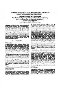
• The ‘Significant Bit Count’ (SBC) is the number of least-significant bits at the bottom of a binary number ignoring all of the most-significant bits which constitute a series of ‘1’s or ‘0’s. These most-significant bits represent only the sign of the number in 2’s complement format. For example: the SBC of 0x00006380 is 15 and the SBC of -5 (0xFFFFFFB) is 3. Figure 1 shows the statistics of the SBC distributions for the benchmark programs. As we can see, the SBC distribution is not balanced. Most inputs have a low SBC of between 0 and 16 bits. These two imbalances in the operand distributions are very important for the design of a low-power multiplier. In the following sections we will introduce a low-power multiplier designed to exploit these unbalanced distributions.
3.
MULTIPLIER ARCHITECTURE
Many different kinds of multipliers have been proposed with very different hardware requirements, throughput and
45
40 ijpeg go compress vortex
35
30
Percentage occurence
Section 2 four benchmark programs are used to investigate the statistics of multiplier input vectors. Section 3 presents the pipelined iterative architecture of the new multiplier. Section 4 compares the power dissipations of Booth’s and radix-2 multipliers and presents a sign-changing algorithm. Section 5 describes the asynchronous control circuit of the new multiplier. Section 6 solves the problem of large registers by splitting the registers into several smaller segments. Section 7 compares the experimental results from four different multipliers. Section 8 concludes and summarizes the low power techniques used in the new multiplier.
25
20
15
10
5
0
0
5
10
15 20 Significant bit count
25
30
Figure 1: SBC distributions for the benchmarks power dissipation. These include: serial multipliers, sequential multipliers, array multipliers and tree multipliers [7]. Serial multipliers and sequential multipliers are rarely used in today’s high-performance CMOS circuits because of their poor throughput, although they are quite power-efficient. Array multipliers and tree multipliers are two of the most popular kinds of multiplier. The basic principles of array and tree multipliers are: • Generate partial products; • Add all the partial products together through several rows of carry-save adder (CSAs) using, for example, 32 (full) adders or 4-2 adders [8], finally obtaining one partial sum and one partial carry; • Send the partial sum and partial carry to a multi-bit carry-propagate adder to get the final result. Array multipliers and tree multipliers are fast but expensive in terms of hardware and power consumption. Iterative structures [8] allow a trade-off between performance and hardware requirement. Pipelining is usually used in iterative systems to improve their performance. The multiplier we propose here, using a pipelined iterative architecture, is illustrated in Figure 2. The design uses a 2-stage pipeline: the first stage is an 8-2 adder tree; the second stage is a 4-2 tree and a 62×2-bit shift register containing the partial sum and carry which it feeds back to the 4-2 adder tree. In this multiplier both first and second adder trees are efficiently reused in every cycle through an iterative algorithm. With a 40 × 2-bit pipelined register row, these two CSA rows operate in parallel, thus improving the multiplier’s throughput by a factor of two. The multiplier calculates 8 partial products in one cycle and completes a 32 × 32-bit multiplication in 4 cycles.
4. RADIX-2 ALGORITHM High-radix algorithms are often used to speed up multipliers by reducing the number of partial products. The most commonly-used high-radix algorithm is the modified Booth’s algorithm [11]. The modified Booth’s algorithm scans the multiplier two bits (instead of one) at a time, so reducing the number of partial products by a factor of two. It has been suggested that Booth’s tree multipliers are
Partial products
8−2 adder tree
Pipeline register2
Pipeline register1
4−2 adder tree
Iterative register1
Iterative register2
Result register
Shift register
Figure 2: A pipelined iterative architecture
less-power efficient than non-Booth tree multipliers [4][5]. However, no explanation was given for this conclusion. Why is the Booth’s algorithm not power-efficient even though it reduces the number of partial products and CSAs? We have identified one reason as follows: With the modified Booth’s algorithm, partial products have a 50% probability to be −1× or −2× the multiplicand. These inverting operations introduce many transitions into the adder tree. For example, if the multiplicand M D is 1, −M D and −2 × M D switch all of the bits up to the most-significant bit, causing 32 transitions in each operation. Based on the statistics presented in Section 2, we know that most operands are small positive numbers. Booth’s algorithm causes a lot of switching activity even for a small multiplication such as 1 × 1, so it is not a good algorithm for use in low-power multipliers. A second reason for questioning its use is that, because of the long wires and high fan-in required in their implementation, the Booth’s encoder and partial-product generator consume a lot of power themselves and generate glitches which propagate through the whole multiplier. Race-free encoding schemes have been proposed to ameliorate this problem [9]. Consequently we consider that Booth’s algorithm should not be used in a low-power multiplier. Although the Booth’s encoder and partial-product generator reduce the number of partial products by a factor of 2, the same result can be achieved by adding another row of 4-2 adders to the adder tree. As shown in Figure 3, two Booth’s select MUXes can be replaced by a 4-2 adder and four AND gates (or 2-1 MUXes). Multiplicand
MUX
MUX
MUX
4−2 adder
MUX
control wires
=
4−2 adder
4−2 adder
4−2 adder
Figure 3: Two kinds of 8-2 adder trees
We can compare the speed and area requirements of these two circuits. Let us take the race-free encoding [9] as an example. A race-free partial-product generator requires 24 transistors. A compact 4-2 adder using double passtransistor logic (DTL) requires 44 transistors [10]. The 2-1 MUX requires 3 transistors. It appears that the non-Booth’s circuit is slightly bigger than the race-free encoding circuit (44 + 3 × 4 > 24 × 2). However, the race-free encoding circuit has four control wires — N EG, ×1, ×2, Z — spreading through the whole partial product generator. If we take the wires into account, the non-Booth’s circuit is smaller than the race-free encoding circuit. Even if we compare the nonBooth’s circuit with a small Booth’s encoding circuit [9], the non-Booth’s circuit incurs less than 5% hardware overhead. In our investigations the non-Booth’s encoding circuit was 18% faster than the Booth’s encoding circuit because the long control wires put heavy loads on their drivers and make the Booth’s encoding circuit slow. The regular structure of the non-Booth’s encoding reduces the possibility of glitches which is good for power-efficiency. We also found that the race-free encoding scheme is only race-free in an ideal situation. Because of the high fan-in, it is hard in practice to ensure that signals arrive at the same time. We developed a software model to compare the switching activities of non-Booth’s and Booth’s tree multipliers. We used the model to calculate the numbers of transitions in 4-2 adders with 10000 positive input numbers of different SBCs. The results are shown in Table 2. Table 2: Numbers of transitions in Booth’s and non-Booth’s multipliers SBC 8 16 24 32 Non-Booth’s 140978 634928 1362437 2221972 Booth’s 490987 1243814 1874260 2511356 Ratio 1/3.50 1/1.96 1/1.38 1/1.13
We can see from Table 2 that, even for random operands, non-Booth’s multipliers are somewhat more power-efficient than Booth’s multipliers. However, with inputs having a small SBC non-Booth’s multipliers are significantly better.
4.1 Sign-changing Algorithm The results in Table 2 are based on the assumption of positive inputs. Although most inputs are positive for the four benchmark programs introduced in Section 2, some applications may have a higher incidence of negative numbers. The low-power advantage of non-Booth’s multipliers will be more convincing if the power-efficiency can be maintained for negative inputs. To achieve this goal we need an algorithm which can change both multiplicands and multipliers to positive if they are negative. We propose a sign-changing algorithm to achieve this objective. The sign-changing algorithm for 32-bit multipliers is based on the following functions: a×b = a×b+a+b+1
(2)
a×b = a×b+b−1
(3)
a×b = a×b+a−1
(4)
We can test the sign of an input by checking its most significant bits (bit 31). If both multiplicand and multiplier
are negative we use Equation (2): invert both multiplicand and multiplier and send them to a non-Booth’s multiplier. For array or tree multipliers, we need another row of 4-2 adders to add a and b. We then get the partial sum and the partial carry. We use a carry-propagate adder to add the partial sum and carry with a carry in of 1. If only one of the operands is negative we use Equation (3) or (4): we invert the negative operand and send it and the positive operand to a non-Booth’s multiplier. We use the additional row of 4-2 adders to add the positive operand and 0xFFFFFFFF (the least significant 32 bits of ‘-1’). However, we are left with the problem of adding 0xFFFFFFFF00000000 (the most significant 32 bits of ‘-1’). We could, of course, have a long 4-2 adder row consisting 64 adders to do this, but this would need a lot of hardware and consume a lot of power. Instead, we distribute the 1s in 0xFFFFFFFF00000000 across the significant bits of the 32 partial products. Figure 4 illustrates the principle.
+
x x x x x x 1 1 1 1
x x x x 0
x x x x x x 0 0 0
=
+
1 x x x x 1 x x x x 1 x x x x 1 x x x x
Figure 4: Distributing the higher-order 1s Using the sign-changing algorithm, the non-Booth’s multiplier retains its low-power advantage for negative operands. However, we need another row of 4-2 adders to add the two extra numbers. Fortunately, for our pipelined iterative architecture we can avoid this overhead by putting these two extra numbers in Iterative Register1 and Iterative Register2 in Figure 2 at the start of the multiplication. For positive inputs we set the Iterative Registers to zero. In the first cycle of multiplication, 4-2 adder row2 just propagates the two partial products from the Pipeline Registers to the Iterative Registers. For negative inputs, the first cycle is used in 4-2 adder row2 to add the two partial products to the two extra numbers. The implementation of the sign-changing algorithm in our pipelined iterative architecture needs only two rows of inverters and MUXes, which represents a very small hardware overhead.
5.
operands they take a short computation time and consume little energy whereas for complex operands they take a long computation time and consume more energy. In Section 2 we presented the unbalanced SBC distributions displayed by the four benchmark programs. An asynchronous multiplier can fully exploit this characteristic to minimize power consumption. The basic principle of out design is as follows: the multiplier takes 4 cycles to finish a multiplication through a pipelined iterative architecture. We divide the 32 bits of a multiplier into 4 groups, 8 bits for each group. So if Bit31 − Bit24 are all 0s or 1s, one cycle of multiplication can be sped up. Similarly, two or three cycles can be sped up if the next one or two groups of eight bits are all the same as the top group. The multiplication cycles can be separated into two kinds — normal cycles and early termination cycles. In normal cycles the multiplier operates as usual, but during early termination cycles the 4-2 compressors are idle and the Iterative Registers simply shift the output to the proper position. This is called an ‘early termination’ algorithm. With the early termination algorithm we can not only save power but also increase the throughput of the multiplier. The asynchronous latch controller used in the multiplier is shown in Figure 5. The latch controller is constructed from two C-elements [13]. It is normally closed, which means that the latch opens only when a new stable value is available on its inputs, preventing unwanted glitches from propagating to the next pipeline stage. Normally-closed latch controllers are good for low power [14]. The latch controller is also fully-decoupled [15], and we can use normal levelsensitive latches to construct an asynchronous pipeline with 100% occupancy. Clocked logic requires edge-triggered registers to construct pipelines with 100% occupancy. As is well known, level-sensitive latches present half the capacitive load of edge-triggered registers to clock signals. In the new multiplier, the Pipeline Registers are level-sensitive latches and the Iterative Registers are edge-triggered registers. The multiplier is a 2-stage pipeline, so its control circuit includes two latch controllers, controlling the Pipeline Registers and the Iterative Registers respectively.
Ain
ASYNCHRONOUS CONTROL
It is often argued by advocates that asynchronous logic offers a more flexible power-management strategy than clocked logic because an asynchronous system only performs processing ‘on demand’ [12]. With asynchronous latch controllers, we can readily close the datapath circuits as soon as they have finished performing their logic functions. This kind of fine-grain control may stop unnecessary switching activity, thus saving power. For clocked circuits, arithmetic functions always have a fixed operation time independent of their inputs. For example, a synchronous multiplier will finish a multiplication in a fixed number of clock cycles even for a simple multiplication such as 1 × 1. Otherwise, it is very difficult for the circuit to achieve pipelined operation. An asynchronous logic block, on the other hand, co-operates with other asynchronous blocks by sending ‘request’ and ‘acknowledgement’ signals, thus avoiding this kind of difficulty. It is in the nature of asynchronous circuits to achieve input-dependent computation, which means that for simple
Aout C
C
Rout
Rin Lt
Figure 5: A normally-closed latch controller To understand fully why the new multiplier consumes less power than its synchronous counterpart, analyzing the operation of the pipeline is very important. Figure 6 illustrates the different pipeline operations of the asynchronous multiplier and a synchronous multiplier under the conditions of (a) 4 normal cycles and (b) 1 normal cycle. Without early termination as shown in Figure 6(a), the synchronous multiplier has some unnecessary switching activity in the first and last cycles: In the first cycle, only pipeline stage1 needs to do useful work, while stage2 should be idle and wait for the data from stage1. In the last cycle, pipeline stage1 has finished its work, and only stage2 needs to calculate the fi-
nal result. However, because in the synchronous multiplier both pipeline register and shift register are connected to the global clock signal, both stages operate simultaneously, thus causing some unnecessary switching activity. With 3 early termination cycles, the synchronous multiplier wastes even more energy in unnecessary activity as shown in Figure 6(b). In conclusion, asynchronous design has a more flexible power-management strategy and will stop activity in some or all of the system whenever its operation is unneeded. It is difficult for synchronous logic to achieve this goal because all the subsystems are driven by the same clock signal. The power in very carefully designed asynchronous circuits is dissipated along the lines of “pay as you go” or “on demand”. The power dissipation only depends on how much work needs to be done.
������ ������ ���� ��� ���� � ��
� � � �
0�/0�/ 0�/0�/ 0/0/ 0/�0�/ 0/ ������ ������ ���� ������ ������ ���� ��� ����� �� �� � ����� ����� ��� ��� ��� �� �� �� �� �� � � �� �� �� �� � � ������ ������ ����
����� ����� ��� ����� )�**)�)�**�) )**)
���� ���� �� �� '�(('�'�((�' '(('
Necessary activity
�� ������������ ����� Stage1 �� Stage2
������ ������ ���� -�..-�- -�..�-.�- -..-.Stage2 .� -�. -�. -. Shift register
2�12�12�1 2�12�12�1 212121 21�21�2�12�1 2121
The proposed multiplier
!�"�! !�"�! !"! "�"�" %�&&%�%�&&�% %&&%
,�,�,�+ ,�,�,�+ ,,,+ ,+�+#��+$ ,�++�#�+$ ,++#+$ $�# $�# $#
4�34�3 4�34�3 == 9�::9�:�9 9�::�9:�9 =ABBABA 9�: 9�: 9: A�B A�B A�B AB
?@� @�?@�@�?? @� @?@@?? ??@� ?C� @?�C�D @� @?CD CD� DC�D�CC�D DD� CC� D DCDCCD
8� 8� 8887 8� 8� 8� 8� 787� 78� 877 7 � � 7 E7� � E FFE7� E7E� EF FF� EF EFFE7EFEF F� F� E�
A synchronous multiplier
(a) Without early termination
(b) 3 early termination cycles
Figure 6: The pipeline operations in the two multipliers
6.
Pass0 Clock
B31−B16
B15−B8
B7−B0
Figure 7: 32-bit split register organization have not seen it applied before to the design of latch- or register-based multipliers.
7. EXPERIMENTAL RESULTS
��������������� ��������������� ��� ��� ��� �� ������ ������ ������ ���� ������ ���� ���� ���� Early termination cycles
Shift register
Stage1
Unnecessary activity
Pass1
SPLIT REGISTERS
In our design we use the PowerPC603 master-slave register [16] in our Iterative Registers. Although the PowerPC register is very power-efficient, and we use small levelsensitive latches for the Pipeline Registers, we still find that the registers and their drivers consume about 58% of the total power. This is because large registers (we have about 200 register bits) put a heavy load on the control wires. The long wires themselves constitute a large capacitance. If we can decrease the capacitance of the registers and wires we can greatly improve the power-efficiency of the multiplier. Because of the unbalanced SBC distribution, in most cases the top 16 bits of Pipeline Register and Iterative Register stay 0 and we do not need to clock them. Therefore we split the registers into 3 groups. The first group is Bit32 − Bit16 , the second group is Bit15 − Bit8 and the third group is Bit7 − Bit0 . The circuit is shown in Figure 7. We use two control wires — P ass0 and P ass1 — to control how many bits should be clocked. Because we already have a cycle detector to detect how many normal cycles a multiplication needs, the only overhead incurred for splitting the registers is 2 MUXes. Testing the split registers by simulating the schematic we found a 12% energy saving. Because the schematic-based simulation does not include wire capacitance we think it likely that in a real circuit splitting the registers will offer a greater power saving. The split-register technique is similar to a technique used previously in a low power register bank [17]. However, we
Four different multipliers were implemented for comparison. They are: a synchronous non-Booth’s multiplier with unified registers (SNN), an asynchronous Booth’s multiplier with unified registers (ABN), an asynchronous non-Booth’s multiplier with unified registers (ANN) and an asynchronous non-Booth’s multiplier with split registers (ANS). The various implementations were simulated using HSPICE, with netlists exported from Cadence Composer-Schematic. A Verilog test harness was constructed to present the input stimuli and to check that the outputs were correct. The multipliers were analyzed under the conditions of a 1.8 volt supply and 27 ◦ C temperature on a 0.18 micron CMOS technology. The input vectors were 1000 pairs of numbers taken randomly from the 4 benchmarks introduced in Section 2. We controled the throughput at 100 million multiplications per second. The results are shown in Table 3. Table 3: Power comparisons among 4 multipliers Multipliers SNN ABN ANN ANS Power (mW) 16.17 9.56 7.35 6.47 Ratio 2.2 1.3 1 0.88
As can be seen from Table 3, the asynchronous multipliers consume less than half the power of their synchronous counterparts. Non-Booth’s multipliers save 23% of the power of those using the modified Booth’s algorithm, and split registers save another 12% of the power. The ANS multiplier completes a multiplication requiring 4 normal cycles in 6.5 ns, resulting in a throughput of 150 million multiplications per second. However, this is the worst case. It completes a multiplication requiring 3 normal cycles in 6.0 ns, a multiplication requiring 2 normal cycles in 5.2 ns, and a multiplication requiring 1 normal cycle in 4.3 ns. Based on the unbalanced SBC distribution, ANS has an average throughput of more than 200 million multiplications per second.
8. CONCLUSION Four benchmark programs were analyzed in order to find the statistics of typical multiplication operands. It was found that the distributions are imbalanced in two ways that are very important for low-power multiplier design: positive operands greatly out-number negative operands, and
the number of significant bits is typically small (fewer than 16). A new design for a low-power multiplier was presented based upon the above observations. The new multiplier uses an area-efficient pipelined iterative architecture. It employs asynchronous control and an early-termination scheme, and has a very flexible way to control the datapath. The new multiplier dissipates power ‘on demand’ — for those small operands, it consumes less power; for large operands, it consumes more power. Our experiments show that asynchronous control reduces the multiplier’s power consumption by more than half. A non-Booth’s algorithm avoids the inverting operations that are necessary in multipliers using the modified Booth’s algorithm, thereby avoiding a lot of signal transitions. A sign-changing algorithm is used to ensure that the nonBooth’s multiplier retains its low-power advantage for negative operands. Compared to a Booth’s multiplier, the nonBooth’s multiplier has a 23% reduced power dissipation. Split registers help the multiplier to save a further 12% of its power dissipation. The total switching capacitance is decreased by splitting a large register into several small segments. In most cases, only a small part of the register is driven by the clock signal on each cycle, thus saving power. The new asynchronous multiplier demonstrates the lowpower advantage of asynchronous logic resulting from its fine-grain control. Although the multiplier is an iterative asynchronous multiplier, the non-Booth’s algorithm used here is equally suited to synchronous multipliers, including array and tree multipliers. The split datapath scheme is also valid for any register- or latch-based multiplier with an unbalanced distribution of input operands.
9.
REFERENCES
[1] S. B. Furber, D. A. Edwards and J. D. Garside. AMULET3: a 100 MIPS Asynchronous Embedded Processor. ICCD’00, 17-20th September 2000. [2] D. Soudris, C. Piguet and C. Goutis (eds). Designing CMOS Circuits for Low Power. Kluwer academic publishers, 2002. [3] A. P. Chandrakasan and R. W. Brodersen. Low Power Digital CMOS Design. Kluwer academic publishers, 1995. [4] T. Callaway and E. Swartzlander. The Power Consumption of CMOS Adders and Multipliers, in Low-Power CMOS Design, A. Chandrakasan and R. Brodersen (eds), IEEE Press, 1998.
[5] L. Bisdounis, D. Gouvetas and O. Koufopavlou. Circuit Techniques for Reducing Power Consumption in Adders and Multipliers, in [2]. [6] J. Hennessy and D. A. Patterson. Computer Architecture — A Quantitative Approach, Third Edition. Morgan Kaufmann Publishers, 2003. [7] Amos. R. Omondi. Computer Arithmatic Systems: Algorithms, Architecture and Implementation. Prentice Hall, 1994. [8] M. Santoro. SPIM: a pipelined 64 × 64-bit iterative multiplier, IEEE Journal of Solid-State Circuits, 1989. [9] R. Fried. Minimizing Energy Dissipation in High-Speed Multipliers, Proc. of International Symposium on Low Power Electronics and Design, 1997. [10] J. Liu, Arithmetic and Control Components for an Asynchronous System, PhD thesis, The University of Manchester, 1997. [11] A. D. Booth, A Signed Binary Multiplication Technique, Quart. Journ. Mech. and Applied Math., vol. 4, part 2, pp. 236 240, 1951. [12] S. B. Furber, A. Efthymiou, J.D. Garside, M.J.G. Lewis, D.W. Lloyd and S. Temple, Power Management in the AMULET Microprocessors, IEEE Design and Test of Computers Journal special issue pp. 42-52 (Ed. E. Macii), March-April 2001. [13] J. Sparsø, S. Furber (eds). Principles of Asynchronous Circuit Design: A systems perspective. Kluwer Academic Publishers, 2001. [14] M. Lewis, J.D. Garside, L.E.M. Brackenbury. Reconfigurable Latch Controllers for Low Power Asynchronous Circuits. Proceedings of Async99, April 1999. [15] S.B. Furber and P. Day, Four-Phase Micropipeline Latch Control Circuits, IEEE Transactions on VLSI Systems, vol. 4 no. 2, June 1996 pp. 247-253. [16] V. Stojanovic and V.G. Oklobdzija. Comparative analysis of master-slave latches and flip-flops for high-performance and low-power systems. IEEE Journal of Solid-State Circuits, April 1999. [17] V. Zyuban and P. Kogge, Split Register File Architectures for Inherently Low Power Microprocessor, Power Driven Microarchitecture Workshop at ISC98, June 1998.