APPLIED PHYSICS LETTERS
VOLUME 76, NUMBER 24
12 JUNE 2000
Low-energy electron beam focusing in self-organized porous alumina vacuum windows T. Doll,a) J. Vuckovic, M. Hochberg, and A. Scherer California Institute of Technology, Pasadena, California 91125
共Received 14 February 2000; accepted for publication 20 April 2000兲 Micromachined, micron-thick porous alumina membranes with closed pore endings show high electron transparency above an energy of 5 keV. This is due to the channeling of electrons along the negatively charged insulating pores after surmounting the thin entrance layer. We also find a sharp hightransparency energy window at energies as low as 2 keV which may be the result of a local maximum of channeling, as predicted by simulations, and positive charge up of the entrance layer causing electron electrostatic focusing. Applications for these membranes range from atmospheric electron spectroscopy to self-assembled, nanoscale, large-area electron collimators. © 2000 American Institute of Physics. 关S0003-6951共00兲04824-5兴
Electron transparent vacuum windows are used in many applications employing an electron beam striking an object that requires an atmospheric or liquid environment, such as living cells inspected with an atmospheric scanning electron microscope. The window is necessary to keep the electron sources in vacuum. Recently, the development of atmospheric electron x-ray spectroscopy 共AEXS兲1 systems for in situ material analysis has begun, making use of the same concept. In the future, one might even think of miniaturizing these systems towards Micro-AEXS. Besides the main issue of mechanical stability, a high transparency at low electron energies is of interest. Design of the membranes is done utilizing a heuristic concept, refined by modeling the interaction of electrons with the material in the structure of choice. We approximate the relation of transmissivity T of a layer of given thickness d and such material properties as atomic number Z and density by T 共 E 兲 ⬀ Z 1/2E ⫺1 f 共 d 兲
共1兲
with f (d) being almost linear up to very high energies.2 This would favor light-element-low-density membranes such as polymers 共see Ref. 3 for an overview兲 or BN, but these materials require a rigid supporting grid4 or have technological difficulties.5 Therefore development has focused on micromachined Si3N4 membranes.6 However, the major drawback of this approach is that a 200 nm minimum thickness1 is required for mechanically stable vacuum windows with 1 mm2 dimensions. In this work we combine a much thinner window layer with the idea of a self-assembled supporting grid by utilizing porous alumina. Although the material does not represent an improvement in terms of transmissivity 共1兲, porous alumina offers very thin membrane sections for efficient electron transmission. Made by anodic oxidation, it consists of a close-packed,7 hexagonal array of parallel pores perpendicular to the surface. The pores diameters can be varied between 40 and 400 nm with processing voltage and have closed a兲
Electronic mail:
[email protected]
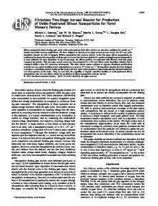
endings in the shape of ‘‘domes’’ with a thickness in similar range, which we will use as an electron entrance. The mechanical stability for vacuum window applications, provided by the pore honeycomb, as well as some general electron transparency has already been shown.8 Figure 1 gives a high resolution scanning electron microscopy 共SEM兲 micrograph of the dome pore endings in cross section. The inset is a proposed model of electron transport by channeling which is expected from charging of the inner pore walls. This study characterizes the electron transparency of porous alumina membranes. We find a significant low energy transmissivity due to channeling in insulating pores. In parallel, we perform a Monte Carlo simulation using the ‘‘single electron’’ approximation9–11 that determines the path of electrons by considering elastic scattering events only. For the high energy range (⬎10 keV) we use Rutherford’s cross section and Bethe’s rule of energy loss, whereas for the lower energy range (⬍10 keV) modifications of both of these were applied.12,13 The membranes were fabricated by anodization of pure aluminum sheets in oxalic acid at 40 V and 0 °C. The open pore side was mechanically polished to remove the starting layer and to achieve desired membrane thickness of either 4 or 10 m. The aluminum was then electrochemically re-
FIG. 1. Cross section of alumina pores with dome pore endings. Inset: Electrons traveling along the charged pores.
0003-6951/2000/76(24)/3635/3/$17.00 3635 © 2000 American Institute of Physics Downloaded 18 Dec 2005 to 131.215.240.9. Redistribution subject to AIP license or copyright, see http://apl.aip.org/apl/copyright.jsp
3636
Doll et al.
Appl. Phys. Lett., Vol. 76, No. 24, 12 June 2000
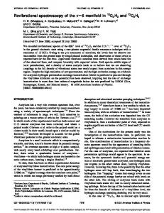
FIG. 2. Electron transmissivity measurement within SEM utilizing Faraday cup.
moved in defined areas, leaving freestanding alumina windows in mechanically stabilizing Al frames. The membranes had 97⫾6 nm interpore spacing in hexagonal array, an average wall thickness of 46⫾5 nm, and a pore/alumina volume ratio of 31%. Over the entire membrane, the pores were randomly tilted by a few degrees from vertical direction within domains of several m size. Transmissivity measurements were setup in a SEM as depicted in Fig. 2. Half cut membranes were mounted on a SEM holder with the bare membrane freely suspended over half of a Faraday cup. This allowed either direct probe current measurements or through the alumina membrane and their ratio provided the electron transmissivity. Care was taken by insulating the membrane from the SEM holder and grounding the aluminum frame in order to avoid disturbing surface currents. Additionally, the SEM was operated without active secondary electron 共SE兲 detection 共SEOFF兲 since the high electric secondary electron attraction field from our Everhart–Thornley detector influenced the transmission measurements at low beam voltages. Mechanical calibration ensured working in the same 45⫻55- m-wide viewing field under SEOFF conditions. The overall variation of transmittance did not typically exceed 10% and stabilized within 90 s. Readings were taken after this for another 90–210 s. Between those measurements 30 min pauses were kept to completely discharge the membranes. Several 10 m and one 4 m samples were tested in both orientations—domes or open pores facing toward incident electrons. The electron energy ranged from 1 to 25 keV. Figure 3 depicts the transmissivity versus SEM beam energy for a 10-m-thick alumina membrane. As a first indicator for channeling we find that the pore ratio of 31% is
FIG. 4. Simulations of electron transmission. The low-energy curve is a convolution of the 共entrance兲 membrane response with an E ⫺1 deflection dependency yielding a peak close to the experimental data. Higher energies have a channeling with less energy dependence.
exceeded even for the tilted pores. The curves for both orientations lie close together except in the low energy range 共1–5 keV兲 where, in ‘‘domes-up,’’ a prominent peak at 2 keV is observed for all samples, which is superimposed onto an almost uniform 10% transmissivity. The peak is still present during SEON, which in all other low energy measurements lowered the transmitted current by a factor of approximately 0.6. Above 5 keV this SE deflection decreases remarkably. Starting from there, transmissivity increases and leads to a saturation voltage around 17 keV for the 4 m membranes. The curve of thick membranes is constantly increasing up to 25 keV. At this energy, the transmission was found to be in the range of 65%–75% for all samples. The simulations of electron scattering in Al2O3 structures of corresponding geometry are shown in Fig. 4. We added to a simple flat 45 nm entrance 共dome兲 membrane 共which alone yields too steep a transmissivity response兲 a pore structure underneath and modeled a redirection of electrons, which enter the pores, towards the pore axis. We neglected the total transmissivity contribution of those electrons that would start inside the pore walls, but they still may affect the subsequent parameters of electrostatic deflection. The latter, being indirectly proportional to the kinetic energy, was modeled by a threshold angle ␣, below which the electrons were set onto the channeling path. Accordingly, for the low energy range, ␣ E⭐50° keV improved the fit and also provided a first low-energy, high-transmissivity peak. It arises from the crossover of the E ⫺1 scattering in the dome membrane with the E favored channeling. However, the proportionality does not hold in the higher energy regime and has to be replaced by a fixed ␣ ⫽7°. In order to obtain channeling in general, we assume a negative charging of the pores that results from a net trapping of electrons inside the pore walls. It is reasonable that any initial charge distribution will deflect other electrons towards uncharged regions until an almost homogeneous distribution is achieved. A value for the necessary, minimum charge density will be one electron placed within a planar unit cell of the hexagonal pore array. For a homogeneous distribution we assume the same lattice constant S in the depth direction and thus approximate a charge density n e ⫽ 共 1/2)S 3 兲 ⫺1 ⫽1.3⫻1015 cm⫺3.
共2兲
FIG. 3. Electron transmissivity of a porous alumina membrane with 10 m For S⫽97 nm, a 10 m membrane thickness and a beam thickness given for both directions of incidence. Arrow: Low energy transcurrent density of 40 mA/m2, charging will be completed in mission maximum. Downloaded 18 Dec 2005 to 131.215.240.9. Redistribution subject to AIP license or copyright, see http://apl.aip.org/apl/copyright.jsp
Doll et al.
Appl. Phys. Lett., Vol. 76, No. 24, 12 June 2000
FIG. 5. Equipotential lines for positively charged domes and negative pore walls, being similar to an electrostatic lens that focuses incident electrons 共from left兲 towards the pore axis.
less than 100 ms. This explains our stable readings. Furthermore, a corresponding effective surface charge of
⫽ 共 /)S 兲 •d•e⫽2.1⫻10⫺3 As/m2
共3兲
situated inside a dielectric of i will cause a potential seen by the incident beam in the order of V Surf⫽ •a/ 共 4 0 共 1⫹ i 兲兲 ,
共4兲
where a is the average diameter of the area exposed to the electron beam. With Al2O3⬇6, the voltage necessary to start channeling is about 470 V, which is low compared to the incident electron energies. In the energy regime below 5 keV the plateau of 7%– 10% for both membrane orientations must be mainly related to SE since they are easily deflected under the high electric field of the SE detection unit. Their low energy makes them almost useless for atmospheric applications. The 2 keV peak, which has higher stability under this field can be related to higher energy electrons. As the peak is only observed in domes up, the domes must play a key role. A second, charge dependent effect may contribute to this increased transparency. Charging happens, when the total electron yield of SE 共␦兲 and backscattered electrons 共兲 differs from one, and, for insulators there exists a low incident energy range with ( ␦ ⫹ )⬎1, where a slight positive charge-up occurs. The upper limit for this, E2, has been calculated12 for alumina as 4 keV, the lower level E1 being a few hundred volts. Therefore we expect the alumina domes to be positively charged below 4 keV incident energy, where
3637
the peak occurs. If we now combine a positively charged entrance membrane in front of negatively charged pores, we obtain a resulting potential distribution that is similar to focusing electrostatic lenses, as shown in Fig. 5. The equipotential lines inside the pores will redirect those electrons surmounting the entrance membrane towards the pore axis, which adds a real focusing to the generally repulsive pore channeling. Moreover, in front of the domes we get an additional, convex potential distribution due to the dome curvature, so that the incident electrons undergo collimation even before hitting the membrane. In this case a self-enhancing charge concentration at the dome centers will occur. On the other hand, in the case of ‘‘pore openings up’’ the electrostatic lens effects are expected to be self-inhibited due to positive pore wall charging and this corresponds to our experimental observation. Our results may be useful for applications that need micromachined electron transparent windows in general, low energy electron filters, or, as the spacing of the pores can be made below 50 nm, as nanoscale fly’s eyes or condensers for electron optics. For the future, it seems to be possible to even manipulate the low energy transmission window by covering the alumina domes with materials of different E2 values. This research was funded by the German Humboldt Foundation, Caltech SURF and JPL DRDF program and also supported by the U.S. AFOSR, Contract No. AFS5XF49620-1-044.-SC. 1
J. Feldman, T. George, and J. Wilcox, NASA Tech. Brief, NPO-20463, 1998. 2 J. L. Goldstein, Scanning Electron Microscopy and X-Ray Microanalysis 共Plenum, New York, 1992兲. 3 Practical Methods in Electron Microscopy, edited by A. M. Glauert 共North-Holland, New York, 1981兲, p. 9. 4 E. F. Fullam, Rev. Sci. Instrum. 42, 245 共1972兲. 5 R. Levy, J. Vac. Sci. Technol. B 6, 154 共1988兲. 6 E. D. Green and G. S. Kino, J. Vac. Sci. Technol. B 9, 1557 共1991兲. 7 A. P. Li, F. Mu¨ller, A. Birner, K. Nielsch, and U. Go¨sele, J. Appl. Phys. 84, 6023 共1998兲. 8 T. Doll, M. Hochberg, D. Barsic, and A. Scherer, Sens. Actuators A 共in print兲. 9 R. Shimizu, Y. Kataoka, T. Ikuta, T. Koshikawa, and H. Hashimoto, J. Phys. D: Appl. Phys. 9, 101 共1976兲. 10 D. F. Kyser and K. Murata, IBM J. Res. Dev. 18, 352 共1974兲. 11 D. C. Joy, Monte Carlo Modeling for Electron Microscopy and Microanalysis 共Oxford University Press, London, 1995兲. 12 R. Browning, T. Eimori, E. P. Traut, B. Chui, and R. F. W. Pease, J. Vac. Sci. Technol. B 9, 3578 共1991兲. 13 G. Love, M. G. Cox, and V. D. Scott, J. Phys. D: Appl. Phys. 11, 7 共1978兲.
Downloaded 18 Dec 2005 to 131.215.240.9. Redistribution subject to AIP license or copyright, see http://apl.aip.org/apl/copyright.jsp