INTERNATIONAL JOURNAL OF DESIGN, ANALYSIS AND TOOLS FOR CIRCUITS AND SYSTEMS, VOL. 1, NO. 1, JUNE 2011
9
Dynamic Power Reduction of Stalls in Pipelined Architecture Processors Pejman Lotfi-Kamran, Ali-Asghar Salehpour, Amir-Mohammad Rahmani, Ali Afzali-Kusha, and Zainalabedin Navabi
Abstract—This paper proposes a technique for dynamic power reduction of pipelined processors. It is based on eliminating unnecessary transitions that are generated during the execution of NOP instructions. The approach includes the elimination of unnecessary changes in pipe register contents and the limitation of boundary movement of transitions caused by inevitable changes in pipe register contents due to insertion of a NOP into a pipelined processor. To assess its efficiency, the proposed technique is applied to MIPS, DLX, and PAYEH processors considering a number of benchmarks. The experimental results show that the techniques can lead to up to 10% reduction in the dynamic power consumption at a cost of negligible (almost zero) speed and (about 0.2%) area overheads. Index Terms—Dataflow architectures, low-power design, pipelined processors, stall.
I. I NTRODUCTION
P
OWER dissipation limits have emerged as a major constraint in the design of microprocessors where the speed has been traditionally the primary goal [1]. At the low end of the performance spectrum, namely in the category of handheld and portable devices or systems, power has always been the more critical design constraint compared to speed constraint [2]-[9]. In battery-powered applications, where the speed is less of a concern, relatively simple RISC (Reduced Instruction Set Computers) like pipelines are often used [10], [11]. Pipelined processors frequently insert NOP (No Operation Performed) instruction to the pipe to eliminate hazards and generate some delays for the proper execution of the instructions [13]. There are three types of hazards which are structural, data, and control [13]. The structural hazard may occur when there are not enough hardware resources for the execution of a combination of instructions. While in processors with simple architectures, this hazard is usually eliminated in the design phase, it occurs in architectures that use more than one functional unit for instruction level parallelism [13], [14]. A data hazard occurs when an instruction needs the result of its prior instruction that is still in the pipeline and its result is not ready. This occurs when there is not enough latency between these two instructions which are considered data dependent. A technique for preventing data hazard is to All authors are with the School of Electrical and Computer Engineering, University of Tehran, Iran. E-mail:
[email protected],
[email protected],
[email protected],
[email protected],
[email protected]. A.-M. Rahmani is also with Computer Systems Lab., Department of Information Technology, University of Turku, Turku, Finland. E-mail:
[email protected].
use a forwarding unit [13]. The forwarding unit detects the dependencies and forwards the required data from the running instruction to the dependent instructions. In some cases, it is impossible to forward the result because it may not be ready. In these situations, using a NOP instruction is inevitable [13], [14]. The last type of hazard is control hazard that occurs when a branch prediction is mistaken or in general, when the system has no mechanism for the branch prediction. There are two mechanisms for handling the control hazard. The first mechanism runs instructions after a branch and flushes the pipe after the misprediction. Generally, flush mechanisms are not cost effective. A better solution to handle the control hazard is to fill the pipe after the jump instruction with specific numbers of NOPs. This mechanism is called delayed jump mechanism and used widely in DSP processors [13], [14]. The NOP instruction does not contribute to any useful work. Therefore, the power consumed for its execution is wasted. Our study indicates that the percentage of dynamic power consumed by NOP instructions in a pipelined processor is considerable. There are many works that have targeted the power optimization of pipelined processors (see, e.g., [17], [26]). Among them, several solutions have been presented to reduce the number of NOP instructions [13]. Even with employing these techniques, still a large number of stalls would remain. Therefore, the power consumption of the processors may be reduced further by reducing the execution of the NOP instruction itself. The aim of this paper is to reduce the dynamic power consumption of a pipelined processor by eliminating the useless transitions that are generated in the pipeline when a NOP instruction passes through pipe stages1 . This is performed by modifying the architecture of RISC processors. The rest of the paper is organized as follows. Section 2 outlines the design of the baseline pipelined processor used in this work while Section 3 motivates the need for a technique for reducing he dynamic power consumption of a pipelined processor when a stall happens. In Section 4, our proposed technique for reducing the dynamic power consumed during a NOP execution is presented. The microarchitectural changes to the baseline pipelined processor for implementing the proposed technique is presented in Section 5. The results are discussed in Section 6 while the summary and conclusions are gven in the last section. 1 A Preliminary version of this work appeared in the Proc. of VLSI Symposium 2008 [15].
INTERNATIONAL JOURNAL OF DESIGN, ANALYSIS AND TOOLS FOR CIRCUITS AND SYSTEMS, VOL. 1, NO. 1, JUNE 2011
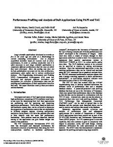
II. BASELINE P IPELINED P ROCESSOR Figure 1 shows the diagram of the microarchitecture of a conventional pipelined processor based on a 5-stage 32-bit Von Neumann MIPS I architecture [13]. While we restrict the discussion to a MIPS like processor architecture, the proposed approach may be applied to other types of architecture. The five stages include: Instruction extraction (FETCH), Instruction decoding (DECODE), Instruction Execution (EXECUTE), Memory access (MEMORY), and Update registers (WRITE BACK). Only two instructions can access the memory. The processor contains 32 registers. In the case of hazard, data hazards are resolved with a bypass unit while branch hazards are resolved by predicting the address results. Interruptions and exceptions are taken care of by a system coprocessor. Furthermore, this processor has 4-way instruction and 4-way data caches. If a hit happens, the data is immediately sent to the next stage while if a miss occurs, the processor should wait for the data to become ready. In the first stage, i.e., FETCH, the next instruction is read from the memory and is loaded into the FE/DE register at the end of this stage. In the second stage, i.e., DECODE, the instruction is decoded where the values of the registers which are needed for running this instruction are read from the register file. In addition, if an immediate value is used in an instruction, the immediate value is properly sign extended or zero filled. It is in this stage that the controlling signals for running the instruction are generated. These controlling signals include the signals for writing to memory and register file as well as the multiplexer selects and the ALU operation type. In the third stage, i.e., EXECUTE, the desired operation is performed on the extracted data in the previous stage. For the branch instruction, the result is computed and based on the computed results, the next value of PC (program counter) is determined. In the forth stage, i.e., MEMORY, depending on the instruction, the desired value is written into a memory location or the content of a memory location is read. In the last stage, i.e., WRITE BACK, based on the instruction, the computed value is written into the register file. In some situations, due to the dependency between the two successive instructions, the data needed for the second instruction should be produced by the first instruction. In these cases, when the second instruction is in the decode stage, the loaded data from the register file are not valid. However, it is possible that when the second instruction actually needs the data in the later stages of the pipeline, the first instruction has produced the data. Therefore, a forwarding unit is added to the pipeline. If a data field is not valid, the forwarding unit tries to forward the valid data from the subsequent stages. In some situations, the first instruction cannot produce the needed data of the second instruction even when this instruction needs the data. In these cases, the second instruction should run with at least a clock cycle delay. Therefore, in the DECODE stage, these cases are determined and a stall is inserted between the two instructions. When a stall is inserted into the pipe, the FETCH stage stops running (PC is not loaded with a new value) and the content of the controlling signals in the DECODE stage are deactivated for a NOP to be inserted
10
into the pipeline. The controlling signals can be divided into two parts which are critical and non-critical. The examples of the critical control signals which should be deactivated for the correct operation of NOP include writing to the memory or register files. The non-critical control signals are those signals that do not effect the correct execution of the NOP instruction, and hence, behave as ”do not care” signals. For the NOP insertion, only the critical control signals ought to be deactivated. III. M OTIVATION F OR O UR A PPROACH After the DECODE stage, the generated control signals are used to control the flow of data. In this stage, if the control unit determines that the current instruction depends on the former instructions and the forwarding cannot resolve the dependency, the control unit inserts a NOP instruction by deactivating the critical control signals of the current instruction including control signals for writing to memory and register file. The NOP instructions are inserted into the pipeline to eliminate hazards. These inserted NOP instructions contribute to the overall dynamic power of a pipelined processor by generating a number of unnecessary transitions. This is explained by an example in our baseline pipelined processor.
Fig. 2.
A simple MIPS program.
A simple program is shown in Figure 2. The first instruction is a LOAD instruction that reads a data from memory and the second instruction is an ADD instruction that uses the loaded data. Because of the dependency between these two instructions, after the LOAD instruction, a NOP instruction should be inserted into the pipeline. During the execution of the simple program of Figure 2, when the LOAD instruction is in the DECODE stage, the control signals and the required data corresponding to this instruction are generated/extracted. On the rising edge of the clock, the generated/extracted control/data are latched into the DE/EX pipeline register. In the next clock cycle, the ADD instruction is in the DECODE stage and the control unit determines that a NOP instruction should be inserted into the pipeline. Therefore, the critical control signals of the ADD instruction are deactivated and these deactivated critical control signals along with the other control signals and the required data of the ADD instruction (current instruction in the DECODE stage) are latched on the rising edge of the clock. Generally, the data parts of the current (i.e., ADD) and previous instruction (i.e., LOAD) are different. It means that data part of NOP is different from the former instruction (i.e., LOAD). Therefore, passing the NOP instruction in the pipe generates a number of transitions. In the third clock cycle, the ADD instruction should be passed to the pipeline. In this time, the control signals corresponding to ADD are generated and latched along with its required data. Since the data and non-critical control signals of NOP and ADD instructions are not the same, the number of transitions
INTERNATIONAL JOURNAL OF DESIGN, ANALYSIS AND TOOLS FOR CIRCUITS AND SYSTEMS, VOL. 1, NO. 1, JUNE 2011
Fig. 1.
11
Dataflow diagram of MIPS pipelined architecture [13].
induced during the passage of the ADD instruction in the pipeline stages is not negligible. This imposes some dynamic power consumption. The objective of this paper is to minimize these transitions. IV. T HE P ROPOSED T ECHNIQUES As discussed, the data part of an inserted NOP instruction is not the same as that of its preceding or subsequent instruction generating a number of transitions. In addition, passing the pending instruction after NOP produces more transitions. These transitions lead to wasting the power consumption which should be minimized. For the NOP instruction to generate as few transitions as possible, its data part should be the same as that of its preceding or subsequent instruction. Because of the unavailability of some of the data of the instruction passing the pipe after NOP, the data part of the instruction preceding NOP should be used as the data part of the NOP instruction. This way, as a NOP instruction passes through a pipe, relative to the previous cycle, the same operations are performed on the same data in all stages of the pipeline minimizing the number of transitions. In addition, the non-critical part of the control signals may be the same as those of the preceding instruction. The proposed idea may be implemented in the DECODE stage by modifying the architecture of the baseline processor as will be explained in Section 5. The technique decreases the number of unnecessary transitions generated when a NOP is inserted into the pipe. When the data part of the instruction before NOP is valid in the DECODE stage, the proposed technique guarantees no useless transitions is generated as a NOP instruction passes through the pipe. However, if parts of the data of the previous
instruction are not valid in the DECODE stage, for the correct execution of this instruction, valid data will be prepared by the forwarding unit. To minimize the number of transitions generated during the execution of NOP in this case, the same data should be prepared for the NOP instruction. If the valid data of the instruction preceding NOP are still in some pipe registers when the NOP instruction needs them, the forwarding unit prepares the data for the NOP as well. In these cases, a few transitions are generated during the execution of the NOP instruction. On the other hand, if the valid data are not available in any pipe registers when the NOP instruction needs them (because the processing of the instruction that generates those data has been finished and has gone out of the pipe), different data are loaded into some operators generating a number of useless transitions which may propagate to the last stage of the pipeline. Here, we propose a technique to prevent the propagation of these transitions to all the pipeline stages. For this purpose, the outputs of the NOP instruction should be the same as its preceding instruction in all the pipe stages to minimize useless transitions. Implementing this technique, the value which is loaded in each pipe register for NOP is the same as that of the previous instruction except for the critical control signals. Therefore, only the critical control signals of pipe registers should be loaded during the execution of NOP instructions. Using this approach, if the data of a NOP instruction are not valid (i.e., the NOP data differ from those of the instruction preceding it) and the valid data are not available in the pipe registers (forwarding unit cannot provide the valid data for the NOP), the change of data which leads to some transitions is inevitable. However, these transitions are propagated until they reach a pipe register where their propagation is stopped because writing into pipe registers has
INTERNATIONAL JOURNAL OF DESIGN, ANALYSIS AND TOOLS FOR CIRCUITS AND SYSTEMS, VOL. 1, NO. 1, JUNE 2011
Fig. 3.
12
Modified MIPS architecture based on the proposed tecniques.
been stopped. Therefore, transitions cannot propagate through the entire pipeline limits the propagation boundary. V. M ODIFICATION O F BASELINE A RCHITECTURE The techniques proposed in the previous section included the case where the data of the preceding instruction of NOP is known and the case where the data of the preceding instruction is not known. To implement the technique based on the first case, it is sufficient to add a load enable control signal to the data and non-critical control parts of DE/EX pipe register. This way, only the critical control signals (such as write to memory and register file signals) that should be loaded in each clock cycle are not controlled by the added load enable signal. When a NOP is decided to be inserted into the pipe, the controller should deactivate the load enable signal. For the second case, a load enable control signal is added to each pipe register after the DECODE stage. This control signal is only applied to data and non-critical control parts of the pipe registers. By deactivating the load enable of a pipe register when NOP results are written into it, only the critical control signals of that pipe register are changed and its other parts remain unchanged. The same as other control signals, these load enable signals are generated by the controller in the DECODE stage and are propagated through the pipe registers like other control signals to the desired destination (i.e., specific pipe register). Figure 3 illustrates the mechanism of propagating the load enable control signals in
the pipe registers. In the DECODE stage, if the controller detects that the current inststruction is dependent on the former instructions and hence a NOP should be inserted into the pipe, the load enable control signals of all upcoming stage registers (i.e., ID/EX, EX/MEM, MEM/WB) are activated. The load enable of ID/EX pipe register is directly fed into it while the load enables of EX/MEM, MEM/WB pipe registers (i.e., LN1 and LN2 respectively) are propagated through pipe registers to reach and fed into the desired pipe register. On the other hand, if the controller does not it necessary to insert a NOP into the pipe, all load enable control signals are deactivated in the DECODE stage. VI. R ESULTS A ND D ISCUSSION In this section, we discuss the power reduction, area overhead, and timing penalty of our proposed power reduction technique. The techniques have been implemented in three general processors: MIPS [13], DLX [13], and PAYEH [14]. MIPS is a 5 stage pipelined processor whose architecture is RISC with fixed-width of 32-bit instructions. The details of this processor can be found in reference [13]. DLX is a text book example of a RISC processor with a 5 stage pipeline using forwarding to avoid data hazards. The DLX processor uses a load-store architecture. All DLX instructions are 32-bit long. It has 32 32-bit registers [13]. PAYEH is a pipelined version of SAYEH [27] with a similar instruction set and has five pipe stages. SAYEH is a multi-cycle RISC processor
INTERNATIONAL JOURNAL OF DESIGN, ANALYSIS AND TOOLS FOR CIRCUITS AND SYSTEMS, VOL. 1, NO. 1, JUNE 2011
13
TABLE I C HARACTERISTICS O F O RIGINAL A ND M ODIFIED MIPS, DLX, AND PAYEH P IPELINED P ROCESSORS Area Characteristic
Frequency Characteristic
Processor
Original Area (µm2 )
Modified Area (µm2 )
Overhead (%)
Original Frequency (MHz)
Modified Frequency (MHz)
Overhead (%)
MIPS
199737.92
200215.89
0.24
50.76
50.76
≈0
DLX
106396.99
106577.86
0.17
80
80
≈0
PAYEH
919530.45
921185.60
0.18
129.33
129.33
≈0
TABLE II P OWER C ONSUMPTIONS OF O RIGINAL AND M ODIFIED MIPS P ROCESSORS F OR D IFFERENT B ENCHMARKS AND I NPUTS Benchmark
Factorial
Fibonacci
Power
Vector Addition
input n=10 n=20 n=30 n=40 n=50 n=10 n=20 n=30 n=40 n=50 n=10 n=20 n=30 n=40 n=50 n=10 n=20 n=30 n=40 n=50
ORG(mW) 502.47 504.98 506.56 506.7 508.07 465.61 471.79 482.33 490.77 503.1 503.79 505.3 505.79 507.11 506.26 515.43 520.23 519.24 521.77 523.63
MOD(mW) 453.43 455.95 457.47 458.77 460.72 427.85 431.97 443.79 446.85 459.18 471.75 473.87 473.98 472.73 475.78 483.58 488.65 483.46 490.72 491.11
IMP(%) 0.0976 0.0971 0.0969 0.0946 0.0932 0.0811 0.0844 0.0799 0.0895 0.0873 0.0636 0.0622 0.0629 0.0678 0.0602 0.0618 0.0607 0.0689 0.0595 0.0621
TABLE III P OWER C ONSUMPTIONS O F O RIGINAL AND M ODIFIED DLX P ROCESSORS FOR D IFFERENT B ENCHMARKS AND I NPUTS Benchmark
Factorial
Fibonacci
Power
Vector Addition
input n=10 n=20 n=30 n=40 n=50 n=10 n=20 n=30 n=40 n=50 n=10 n=20 n=30 n=40 n=50 n=10 n=20 n=30 n=40 n=50
ORG(mW) 600.45 603.45 605.34 605.51 607.14 561.06 568.507 581.2077 591.3779 606.2355 604.548 606.36 606.948 608.532 607.512 628.8246 634.6806 633.4728 636.5594 638.8286
MOD(mW) 564.00 567.24 569.75 564.82 568.71 523.75 529.9622 546.8583 552.9383 569.8007 571.2979 574.1623 574.2335 572.6895 575.0709 598.8297 603.2639 604.9032 604.0312 606.1206
IMP(%) 0.0607 0.06 0.0588 0.0672 0.0633 0.0665 0.0678 0.0591 0.065 0.0601 0.055 0.0531 0.0539 0.0589 0.0534 0.0477 0.0495 0.0451 0.0511 0.0512
TABLE IV P OWER C ONSUMPTIONS OF O RIGINAL AND M ODIFIED PAYEH P ROCESSORS F OR D IFFERENT B ENCHMARKS A ND I NPUTS Benchmark
Factorial
Fibonacci
Power
Vector Addition
input n=10 n=20 n=30 n=40 n=50 n=10 n=20 n=30 n=40 n=50 n=10 n=20 n=30 n=40 n=50 n=10 n=20 n=30 n=40 n=50
ORG(mW) 1065.236 1070.558 1073.907 1074.204 1077.108 963.8127 976.6053 998.4231 1015.894 1041.417 1027.732 1030.812 1031.812 1034.504 1032.77 1082.403 1092.483 1090.404 1095.717 1099.623
MOD(mW) 972.4543 975.278 978.2221 988.1603 981.5689 885.4547 897.4026 908.9644 936.5526 953.7297 949.5212 956.3874 951.6398 958.158 956.0356 1004.47 1007.816 1011.677 1018.688 1017.261
IMP(%) 0.0871 0.089 0.0891 0.0801 0.0887 0.0813 0.0811 0.0896 0.0781 0.0842 0.0761 0.0722 0.0777 0.0738 0.0743 0.072 0.0775 0.0722 0.0703 0.0749
with 16-bit data and 16-bit address buses. PAYEH architecture uses a forwarding unit. This forwarding unit can resolve all dependencies by forwarding the required data from the next pipe stages to the previous ones. The original and modified processors were synthesized by Synopsys D.C. using 130nm TSMC library. Table I shows the reported area and frequency of these processors. As expected, the proposed method does not have any adverse effect on the frequency of the processors. This is due to the fact that the method does not affect the critical paths. Table I also reveals that the hardware overhead of the proposed technique is negligible (< 0.3%). Four benchmark programs were used to measure the effectiveness of the proposed dynamic power reduction technique. The Factorial benchmark reads a number and calculates its factorial while Fibonacci benchmark reads a number and computes Fibonacci series up to the requested element. Power benchmark reads two numbers, a and b, and calculates a to power b (i.e., ab) and Vector Addition benchmark reads two vectors and calculates their addition element by element. These benchmark programs were applied to the original and modified synthesized processors. Every benchmark program was run five times, each time with a different input size. The input size determines the run-time complexity of the program. Input n = 10 (50) corresponds to the least (most) complex runtime.
INTERNATIONAL JOURNAL OF DESIGN, ANALYSIS AND TOOLS FOR CIRCUITS AND SYSTEMS, VOL. 1, NO. 1, JUNE 2011
As Table II indicates, for the MIPS processor, a maximum dynamic power reduction of 9.76% was achieved. The average power reduction of the proposed approach was about 7.66% for this processor. The table shows that as the complexity of a program increases, the dynamic power that is consumed by the processors also increases. Almost the same results were achieved for DLX and PAYEH processors. For the DLX processor, as Table III indicates, a maximum and average power reduction of 6.22% and 5.69%, respectively, were achieved. For the PAYEH processor, 8.86%, and 8.04%, respectively, were the percentages of the maximum and average power savings. VII. C ONCLUSION In this work, we proposed a method for minimizing unnecessary transitions that are generated when a NOP instruction is inserted into the pipe of a pipelined processor. The proposed approach consisted of two techniques. The first one focused on eliminating unnecessary changes in the pipe register contents while the second one restricted the propagation boundary of transitions caused by inevitable changes in the pipe register contents due to insertion of a NOP instruction. To determine the efficacy of the proposed technique, we applied some benchmarks to MIPS, DLX and PAYEH pipelined processors. While the hardware overhead and timing penalty of the proposed approach was negligible, the dynamic power reductions of up to 10% were achieved. R EFERENCES [1] “International Technology Roadmap for Semiconductor,” 2007. [2] V. Venkatachalam and M. Franz, “Power reduction techniques for microprocessor systems,” ACM Computing Surveys, vol. 37, no. 3, pp. 195–237, September 2005. [3] D. M. Brooks et al., “Power-aware microarchitecture: design and modeling challenges for next-generation microprocessors,” IEEE Micro, vol. 20, no. 6, pp. 26–44, November/December 2000. [4] R. Gonzalez and M. Horowitz, “Energy dissipation in general purpose microprocessors,” IEEE Journal of Solid-State Circuits, vol. 31, no. 9, pp. 1277–1284, September 1996. [5] M. Kandemir et al., “Register relabeling: A post-compilation technique for energy reduction,” in Proc. of Workshop on Compilers and Operating Systems for Low Power, October 2000. [6] M. T.-C.Lee et al., “Power analysis and minimization techniques for embedded DSP software,” IEEE Transactions on Very Large Scale Integration (VLSI) Systems, vol. 5, no. 1, pp. 123–135, March 1997. [7] T. Li and C. Ding, “Instruction balance and its relation to program energy consumption,” in Proc. of Intl. Workshop on Languages and Compilers for Parallel Computing, August 2001, pp. 71–85. [8] W. Zhang et al., “Exploiting VLIW schedule slacks for dynamic and leakage energy reduction,” in Proc. of the 34th Annual Intl. Symp. on Microarchitecture (Micro), December 2001, pp. 102–113. [9] M. Sarrafzadeh et al., “Low power light-weight embedded systems,” in Proc. of the international symposium on Low power electronics and design, October 2006, pp. 207–212. [10] J. Montanaro et al., “A 160-MHz, 32-b, 0.5-W CMOS RISC microprocessor,” IEEE Journal of Solid-State Circuits, vol. 31, no. 11, pp. 1703– 1714, November 1996. [11] IBM/Motorola, PowerPC 405CR User Manual. [12] M. A. Amiri et al., “Design and implementation of a 50MHZ DXT CoProcessor,” in Proc. of EuroMicro Conference on Digital System Design Architectures, Methods, and Tools, August 2007, pp. 43–50. [13] D. A. Patterson and J. L. Hennessy, Computer Architecture: A Quantitative Approach. Morgan-Kaufmann, 4th ed. [14] S. Shamshiri et al., “Instruction-level test methodology for CPU core self-testing,” ACM Transactions on Design Automation of Electronic Systems, vol. 10, no. 4, pp. 673-689, October 2005.
14
[15] P. Lotfi-Kamran et al., “Stall power reduction for pipelined architecture processors,” in Proc. of VLSI Design, January 2008, pp. 541–546. [16] A. Hartstein and T. R. Puzak, “The optimum pipeline depth considering both power and performance,” ACM Transactions on Architecture and Code Optimization, vol. 1, no. 4, pp. 369–388, December 2004. [17] S.-J. Ruan et al., “Bipartitioning and encoding in low-power pipelined circuits,” ACM Transactions on Design Automation of Electronic Systems, vol. 10, no. 1, p. 24-32, January 2005. [18] M. Monchiero et al., “Power-aware branch prediction techniques: a compiler-hints based approach for VLIW processors,” in Proc. of ACM Great Lakes symposium on VLSI, April 2004, pp. 440–443. [19] D. Parikh et al., “Power issues related to branch prediction,” in Proc. of International Symposium on High-Performance Computer Architecture, February 2002, pp. 233–244. [20] R. I. Bahar and S. Manne, “Power and energy reduction via pipeline balancing,” in Proc. of the 28th Annual International Symposium on Computer Architecture, June-July 2001, pp. 218–229. [21] A. Correale, “Overview of the power minimization techniques employed in the IBM PowerPC 4xx embedded controllers,” in Proc. of the ACM/IEEE International Symposium on Low Power Design, April 1995, pp. 75–80. [22] V. Tiwari et al., “Guarded evaluation: pushing power management to logic synthesis/design,” IEEE Transactions on Computer Aided Design of Integrated Circuits and Systems, vol. 17, no. 10, pp. 1051–1060, October 1998. [23] H. Kapadia et al., “Reducing switching activity on datapath buses with control-signal gating,” IEEE Journal of Solid-State Circuits, vol. 34, no. 3, pp. 405–414, March 1999. [24] M. Mnch et al., “Automating RT-level operand isolation to minimize power consumption in datapaths,” in Proc. of the Design, Automation and Test in Europe Conference and Exhibition), March 2000, pp. 624– 633. [25] G. Kucuk et al., “Low-complexity reorder buffer architecture,” in Proc. of International Conference on Supercomputing, June 2002, pp. 57–66. [26] S. Manne et al., “Pipeline gating: speculation control for energy reduction,” IEEE Transactions on Computer-Aided Design of Integrated Circuits and Systems, vol. 17, no. 11, pp. 1061–1079, November 1998. [27] Z. Navabi, Digital design and implementation with field programmable devices. Kluwer Academic Publisher, 2004.
Ali-Asghar Salehpour received B.S. degree from Shahed University, Iran, in 2006, and M.S. degree from the University of Tehran, Tehran, Iran, in 2009, both in Computer Engineering. His research interests include low-power design, network, wireless sensor networks, and network security.
Amir-Mohammad Rahmani received his Master degree in computer architecture from Department of Electrical and Computer Engineering, University of Tehran in 2009. He is currently pursuing his research in Computer Systems Laboratory, University of Turku, Finland and has a Ph.D. position in Turku Center for Computer Science (TUCS). His research interests include Low-Power Design, Networks-onchip, Multi-Processor System-on-chip, and 3D ICs. His PhD thesis is focused on Power Analysis and Optimization in 3D-Networks-on-Chip. Amir is a member of IEEE, IEEE Circuits and Systems Society, and EUROMICRO and has published dozens of refereed papers in prestigious books, journals and conferences.
INTERNATIONAL JOURNAL OF DESIGN, ANALYSIS AND TOOLS FOR CIRCUITS AND SYSTEMS, VOL. 1, NO. 1, JUNE 2011
Ali Afzali-Kusha received his B.Sc., M.Sc., and Ph.D. degrees all in Electrical Engineering from Sharif University of Technology, University of Pittsburgh, and University of Michigan in 1988, 1991, and 1994, respectively. From 1994 to 1995, he was a Post-Doctoral Fellow at The University of Michigan. Since 1995, he has joined The University of Tehran, where he is currently a Professor of the School of Electrical and Computer Engineering and the Director of Low-Power High-Performance Nanosystems Laboratory. Also, on a research leave from the University of Tehran, he has been a Research Fellow at University of Toronto and University of Waterloo in 1998 and 1999, respectively. He has published more than 200 technical papers. Dr. Afzali-Kusha, who is a senior member of IEEE, currently serves as an associate editor for the ACM Transactions on Design Automation of Electronic Systems. His current research interests include network-on-chip, low-power high-performance design methodologies from the physical design level to the system level for nanoelectronics era.
15
Zainalabedin Navabi Dr. Zainalabedin Navabi is a professor of electrical and computer engineering at the University of Tehran, and an adjunct professor at Worcester Polytechnic Institute, Worcester, MA, USA. He is the author of eight books on VHDL, Verilog and related tools and environments. Dr. Navabis began his work in the EDA area in 1976, when he started the development of a register-transfer level simulator for one of the very first HDLs. In 1981 he completed the development of an RTL synthesis tool. Since 1981, Dr. Navabi has been involved in the design, definition and implementation of HDLs. He has written numerous papers on HDLs, design automation, and digital system test. He started one of the first HDL courses in the US in 1990, and has since conducted short courses and tutorials in the United States and abroad. In addition to being a professor, he is also a consultant to CAE companies. Dr. Navabi received his M.S. and Ph.D. from the University of Arizona in 1978 and 1891, and his B.S. from the University of Texas at Austin in 1975.