Darren C. Cronquist, Chris Fisher, Miguel Figueroa, Paul Franklin, Carl Ebeling. Department of Computer Science and Engineering. University of Washington.
Architecture Design of Recon gurable Pipelined Datapaths� Darren C. Cronquist, Chris Fisher, Miguel Figueroa, Paul Franklin, Carl Ebeling Department of Computer Science and Engineering University of Washington Box 352350 Seattle, WA 98195-2350
Abstract This paper examines recon gurable pipelined datapaths (RaPiDs), a new architecture style for computation-intensive applications that bridges the cost/performance gap between general purpose and application speci c architectures. RaPiDs can provide signi cantly higher performance than general purpose processors on a wide range of applications from the areas of video and signal processing, scienti c computing, and communications. Moreover, RaPiDs provide the exibility that doesn't come with application-speci c architectures. A RaPiD architecture is optimized for highly repetitive, computationally-intensive tasks. Very deep application-speci c computation pipelines can be con gured that deliver very high performance for a wide range of applications. RaPiDs achieve this using a coarse-grained recon gurable architecture that mixes the appropriate amount of static con guration with dynamic control. We describe the fundamental features of a RaPiD architecture, including the linear array of functional units, a programmable segmented bus structure, and a programmable control architecture. In addition, we outline the oorplan of the architecture and provide timing data for the most critical paths. We conclude with performance numbers for several applications on an instance of a RaPiD architecture.
1: Introduction Many applications from a variety of elds including signal processing, scienti c computing, graphics, and communications represent great challenges for today's compiler and architecture designers. Enormous data sets and large computational requirements push compiler and architecture capabilities to the limit. The importance of e�cient execution is seen in algorithms such as motion estimation for real-time video encoding and accurate low-power ltering for wireless communications. Such computation-intensive applications have been targeted to a variety of di�erent architectures including general purpose processors, application speci c integrated circuits, and eld programmable compute engines. Each of these approaches makes tradeo�s between the range supported applications and performance. The most exible architectures are general purpose processors, including the large class of digital signal processors (DSPs). To achieve performance for a wide range of applications, general purpose processors dedicate a substantial amount of die area to data This work was supported in part by the DARPA under Contract DAAH04-94-G0272, and in part by Tektronix. D. Cronquist was supported in part by a Gray fellowship. P. Franklin was supported in part by an NSF fellowship and in part by an Intel Foundation fellowship. �
From Advanced Research in VLSI (ARVLSI-99), pp 23-40, 1999.
2
and instruction caches, a crossbar interconnect of the functional units, and complex on-line analyses such as speculative execution and branch prediction. These complex mechanisms can extract a moderate amount of instruction-level parallelism from ordinary programs but are not meant to extract the large amount of ne-grained parallelism available in many compute-intensive applications. At the other end of the exibility spectrum lie application speci c integrated circuits (ASICs) which have long been used to achieve higher performance at a lower cost than general purpose processors. High performance can be achieved since the architecture can be tailored for a speci c application to extract the available ne-grained parallelism, while optimizing for power and/or die area. However, the drawbacks of ASICs are their lack of exibility and their high non-recurring engineering costs. By de nition, an application speci c architecture speeds up only one application. This in exibility combined with a high design cost make them unattractive except for very well-de ned and wide-spread applications. Compounding this problem is the fabrication expense that can reach $100k, a cost that makes the use of ASICs reasonable only in high volumes. Field programmable computing has attracted a lot of attention recently because of its promise to bridge the exibility and performance gaps between general purpose processors and ASICs. A eld programmable architecture is like an electronic lego construction set. The user puts legos (called logic blocks) together to form a circuit that best suits his current application. At any time, the user can construct a new circuit by taking apart the old one and building from scratch. As a result, con gurable computing machines can deliver, in theory, the high performance provided by application speci c hardware along with the
exibility of general purpose processors. Unfortunately, this promise has yet to be realized in spite of some successful examples [1, 11]. There are two main reasons for this. First, con gurable computing platforms are currently implemented using commercial eld programmable gate arrays (FPGAs). FPGAs are necessarily very ne-grained (i.e. all of the logic blocks are small and regular) so they can be used to implement arbitrary circuits, but the overhead of this generality is expensive in both area and performance. While general purpose processors use highly optimized functional units that operate in bit-parallel fashion on long data words, FPGAs are very ine�cient for ordinary arithmetic and only somewhat better for logical operations. FPGA-based computing has an area/performance advantage only on complex bit-oriented computations or complicated bit-level masking and ltering. Second, programming an FPGA-based con gurable computer is akin to designing an ASIC. The programmer either uses synthesis tools that deliver poor density and performance or designs the circuit manually, which requires both intimate knowledge of the FPGA architecture and substantial design time. Neither alternative is attractive, particularly for simple computations that can be described in a few lines of C code. Our response to these problems is a new architecture style { recon gurable pipelined datapaths (RaPiDs). RaPiDs are coarse-grained eld programmable architectures for constructing deep computational pipelines. As compared to a general purpose processor, a RaPiD can be thought of as a superscalar architecture with hundreds of functional units but with no cache, register le, or crossbar interconnect. Instead of a data cache, data is streamed in directly from external memory or sensors. Instead of an instruction cache, programmed controllers generate a small instruction stream which is decoded as it ows in parallel with the datapath. Instead of a global register le, data and intermediate results are stored locally in registers and small RAMs, close to their destination functional units. Instead of a crossbar, a programmable interconnect is con gured to forward data between speci c functional units on a per application basis.
3
From Advanced Research in VLSI (ARVLSI-99), pp 23-40, 1999.
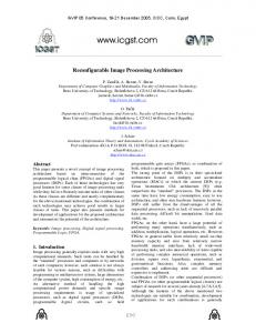
Removing caches, crossbars, and register les frees up a tremendous amount of area that can be dedicated to compute resources, and reduces the communication delay by shortening wires. Unfortunately, these removals also reduce the types of applications that can be computed on RaPiDs. Highly irregular computations, with complex addressing patterns, little reuse of data, and an absence of ne-grained parallelism will not map well to a RaPiD architecture. However, regular computation-intensive tasks like those found in digital signal processing, scienti c computing, graphics, and communications will reap great performance gains on RaPiDs over general purpose processors. In addition, a RaPiD provides the exibility that doesn't come with an ASIC. The fundamental architectural features of RaPiDs have been developed in parallel with a programming language and compiler since a strong synergy exists between architecture, speci cation, and compilation. The user must be able to easily take advantage of the full capabilities of the architecture. In addition, the architecture must have facilities for easing the compilation of a given speci cation. To this end, specialized hardware is added to the architecture and special constructs are added to the language with the ultimate goal of making speci cation simple, compilation feasible, and hardware utilization high. Details of speci cation and compilation can be found in [3]. This paper describes the RaPiD architecture in detail. The block diagram in Figure 1 breaks down RaPiD into a datapath, a control path, an instruction generator, and a stream manager. This paper discusses the fundamental features of each of these components. In particular, Section 2 introduces the datapath architecture, including how functional units and buses are used to form an application's datapath. Section 3 presents a novel architecture for the generation of control for the datapath, including details on the programmed controller architecture for instruction generation. Section 4 discusses how RaPiD interfaces with external memory through the stream manager. Finally, Section 5 introduces a benchmark architecture, and Section 6 analyses area, clock rate, and power requirements of this architecture in a speci c technology. External Memory Input Streams
...
External Sensors
STREAM MANAGER
Output Streams
...
CONFIGURABLE INTERCONNECT From External Memory or A/D
F I F O
F I F O
A L U
M U L T
R A M
R E G
A L U
R A M
R E G
User Def. FU
M U L T
...
R E G
A L U
M U L T
R A M
R E G
F I F O
F I F O
To External Memory or D/A
CONFIGURABLE INSTRUCTION DECODE KEY
Instruction Generator
Data bus One or more control bits
RaPiD Architecture Block Diagram. The RaPiD datapath is a linear pipeline con gured from a linear array of functional units by means of a con gurable interconnect. The instruction generator produces a stream which is decoded by the control path. The resulting decoded instructions provide time-varying control for the datapath. The stream manager communicates with external memory (or memory-mapped external sensors) to stream data in and out of the RaPiD datapath.
Figure 1:
From Advanced Research in VLSI (ARVLSI-99), pp 23-40, 1999.
4
2: RaPiD datapath architecture A typical RaPiD datapath contains hundreds of functional units, ranging in complexity from a simple general purpose register to a multi-output booth-encoded multiplier with a con gurable shifter. The ability of the architecture to forward results between these functional units determines, in part, the range of applications that can be targeted. The interconnection method employed by many of today's superscalar processors is a crossbar { a completely exible interconnect (any functional unit can forward results to any other) which greatly simpli es instruction scheduling ([7]). Unfortunately, the chip area of the crossbar scales with the square of the number of functional units. To avoid this area expense, RaPiD borrows from FPGA architectures by interconnecting its functional units via a con gurable, segmented bus structure. Since RaPiDs consist of coarse-grained, word-based functional units, the interconnect di�ers from that of FPGAs. The buses are word-based instead of bit based and are arranged linearly as opposed to two-dimensionally. A linear structure is easily manageable; it simpli es the layout and reduces the control requirements. Functional units can be more tightly spaced, and there is no need for corner turning switches. Moreover, a wealth of research exists showing how multidimensional algorithms can be mapped to linear arrays [6, 10, 8], especially if some memories are embedded in the datapath since local memory can act like an extra dimension for deeply nested speci cations. The linear structure of the RaPiD datapath was shown in Figure 1. RaPiDs are targeted at word-based computations. The data-width, as well as the choice of xed-point or oating-point, are architectural design parameters. In most cases, the xed-point data width is between 8 and 32 bits, and both signed and unsigned data are supported. Multiple xed-point representations (within the same width) can be provided by con gurable shifters in the datapath. For example, it is often necessary to have a shifter follow a multiplier to allow the correct xed-point representation to be chosen for the multiplier output. Operation errors like over ow cannot be handled as in normal processors. Instead, an extra tag bit is associated with each data value. The functional units can be con gured to set the tag when an over ow occurs. The tag could be used to represent an error state which would be propagated through all future computations. Alternatively, the tag could indicate a saturated value, allowing for further computation.
2.1: Functional units
Each functional unit inputs a set of words from the con gurable interconnect, performs a computation based on a set of control bits, and outputs results in the form of data words and status bits. The status outputs allow for data-dependent control to be generated. A generic functional unit is shown in Figure 2a. All functional unit outputs pass through a Con gDelay unit which can be con gured as 0 to 3 register delays, as shown in Figure 2b. These optional registers allow for the creation of very deep pipelines. A variety of functional units can be included in a RaPiD architecture. General-purpose functional units like ALUs, multipliers, shifters, and memories are the most common, but for speci c domains, a special-purpose functional unit which performs a single function (i.e. has no control inputs) might make the most e�cient use of silicon. An example is a Viterbi decoder for communication applications. For other domains, a highly con gurable functional unit might be the right choice. For example, a functional unit could be constructed of FPGA-like logic blocks to support a range of bit manipulations like nd rst one, count ones, and normalize.
5
From Advanced Research in VLSI (ARVLSI-99), pp 23-40, 1999. w
Data Inputs
w Control Inputs
w
... ...
... Core Computation
w
...
ConfigDelay ConfigDelay
ConfigDelay
(a)
Data Outputs
1
w
...
ConfigDelay
0
w
...
N
2
Status Outputs
N
N
N
N
3
(b)
A Generic Functional Unit and a Con gurable Delay. (a) Each functional unit has inputs and outputs for both data and control. Each output passes through a Con gDelay unit. (b) A Con gDelay unit's N -bit output is equivalent to its input delayed by up to 3 registers, as determined by the two multiplexer control bits.
Figure 2:
Memories within the datapath provide space for temporary variables, constant tables, and con gurable-length delay lines. The size of memory is an implementation parameter. Our experience has shown that for applications we have programmed, a local memory with 3N entries is su�cient for pipelines with N stages. Section 5 examines several functional units that are used in the benchmark architecture.
2.2: Con gurable interconnect
The con gurable interconnect consists of a set of T segmented tracks that run the entire length of the datapath. Each track contains a set of bus segments, some of which are connected by bus connectors { con gurable connections that can be open or up to three register delays. All buses have the same width, which matches the data width operated on by the functional units. Some functional units may require or produce double-width data values, which are communicated via two buses. These values can be treated as two independent single-width values and routed independently, for example, to two di�erent ALUs for double-precision accumulation. An input to a functional unit can be zero (GND) or any one of the T tracks from the interconnect. To accomplish this, each data input is driven by a (T + 1) : 1 multiplexer, whose dlg(T + 1)e select lines are driven by control signals as shown in Figure 3. The zero input can be used, for example, to clear registers. RaPiD allows each functional unit output to drive an arbitrary number of buses via T tristate drivers which are con gured using T control bits. Since each tristate driver is con gured independently, an output can fan out to several buses or none at all if the functional unit is unused. A RaPiD datapath is usually divided into identical units, called cells, which are replicated to form a complete datapath. For example, the simple cell shown in Figure 4 consists of three 1-input functional units with no control inputs (FU1s), three 2-input functional units with two control inputs and one control output (FU2s), seven tracks, and six bus connectors. The number of cell replications performed to complete the datapath is an architectural design decision which depends on the target technology and the application domain's performance requirements. This division of the datapath into cells is invisible when it comes to mapping applications. The rst several tracks of the interconnect have bus segments of di�ering lengths to allow for many types of data forwarding. However, having xed-length bus segments in all tracks is too restrictive for many situations. For example, a pipelined bus carrying data across the entire array is very common. Moreover, the mapping problem simpli es when the lengths of the bus segments can be varied from application to application. To support
6
From Advanced Research in VLSI (ARVLSI-99), pp 23-40, 1999. Input to Functional Unit
Output from Functional Unit
Simplified Representaion Input to Functional Unit
Output from Functional Unit
w w
w w
w
w
w
...
...
w
...
...
w w
w
w
w
w
w
w ...
(a)
(b)
Interconnect Between Functional Units and Buses. (a) Each data input uses a T + 1) : 1 multiplexer to select a bus. Each data output uses T tristate drivers to select the buses to
Figure 3: (
drive. (b) This equivalent but simpli ed representation uses a single line to represent a multiplexer for inputs and tristate drivers for outputs.
con gurable length segments, several of the tracks are populated with bus connectors (Figure 4b). A bus connector can drive left, drive right, or be disconnected. The connection is bu�ered to reduce delay in high fanout signals and can also be con gured to provide up to three register delays.
3: RaPiD control architecture The previous section focused on the architectural requirements for interconnecting a RaPiD architecture's functional units. A speci c interconnect is determined by the many control bits found in the multiplexers, tristate drivers, Con gDelay units, bus connectors, and functional units. Table 1a examines the control requirements for the cell of Figure 4a. Since there are seven tracks, each multiplexer requires three control bits, and each functional unit data output requires seven tristate drivers. Each bus connector and every functional unit output (data and control) have a Con gDelay unit which requires two control bits. The total number of control bits required for this example is 117. Table 1b shows that a single RaPiD-Benchmark cell requires 396 control bits, and hence a 16-cell datapath for would require 6336 bits. There are several approaches for generating the control for this architecture. The most straightforward method is to treat all control as eld programmable con guration bits like in an FPGA. Unfortunately, this approach is too in exible and only applies to algorithms that can be mapped to a purely static data ow network. Any application that requires, for example, a register to be cleared, a RAM address to be incremented, or an ALU operation to be changed on a speci c cycle needs control that can change on each cycle. Another approach for control generation is a programmed control architecture with a 6Kb wide instruction stream. Unfortunately, generating such a wide instruction on every cycle
7
From Advanced Research in VLSI (ARVLSI-99), pp 23-40, 1999.
FU2
FU1
FU2
FU1
FU2
FU1
drive left? Control
Control
0 1
Control ConfigDelay
w BC
w
BC BC
BC BC
BC
drive left?
(a)
drive right?
(b)
RaPiD Datapath Cell. (a) This example cell has seven tracks, six functional units, and six bus connectors. Replicas of this cell are cascaded horizontally to form the entire datapath. (b) A bus connector can drive left, right, or be left unconnected. It can be used to bu�er the signal between adjacent bus segments or to create up to three register delays via the Con gDelay unit. Figure 4:
Control Requirements. (a) The example cell in Figure 4 requires 117 control bits. (b) The RaPiD-Benchmark cell from Section 5 requires 396 control bits. Table 1:
(a) Bits Units Bits Unit Unit Cell Cell Soft Hard Multiplexer 3 9 27 27 0 Tristate Driver 1 42 42 0 42 Con gDelay 2 15 30 0 30 Bus Connector 2 6 12 0 12 FU1 0 3 0 0 0 FU2 2 3 6 6 0 Total 117 33 84
(b)
Bits Units Bits Unit Unit Cell Cell Soft Hard Multiplexer 4 20 80 80 0 Tristate Driver 1 196 196 0 196 Con gDelay 2 26 52 0 52 Bus Connector 2 15 30 0 30 GP Register 0 6 0 0 0 ALU 7 3 21 18 3 RAM 3 3 9 6 3 Multiplier 8 1 8 0 8 Total 396 104 292
would be prohibitively expensive. Our solution is to divide the control into hard control, which is xed for the duration of an application, and soft control, which can change on every cycle. A small percentage of the control bits in a RaPiD architecture need the exibility of soft control. By making the multiplexer control bits soft, the tristate driver control can be made hard. This retains the ability to perform dynamic data forwarding and avoids the extra delay introduced by dynamically controlled tristate drivers. In addition, the Con gDelay unit's control is hard since the amount of pipelining in the datapath tends to be xed over the course of an application. Functional units divide their control between hard and soft depending on the required exibility. The nal two columns of Table 1 divide the control into soft and hard bits for both the example cell and the RaPiD-Benchmark cell. As seen in Table 1, approximately 25% of the a RaPiD's control is soft and the remaining 75% are eld programmable via SRAM bits as in an FPGA. However, only if the soft control can be generated e�ciently, in terms of area and speed, will applications be able to reap the performance bene ts of a RaPiD architecture. A RaPiD's application domain consists of pipelined computations which are very repetitive. Apart from initialization, nalization, and boundary processing, algorithms spend
8
From Advanced Research in VLSI (ARVLSI-99), pp 23-40, 1999.
most of their time in deeply nested computation kernels. Such applications are naturally represented by the composition of deeply nested loops (see [3]). Soft control is statically compiled from the nested loop speci cation. The challenging requirements of soft control are low instruction bandwidth and fast instruction generation. Figure 5 examines possible control architectures. The rst method is to convert the required soft control into a set of state machines, which could then be mapped to an FPGA. This approach, shown in Figure 5a, can take advantage of traditional synthesis techniques for optimizing control. However, this is a more ine�cient approach than using dedicated counters and comparators, as found in the programmed controller approach of Figure 5b since much of the control state comes from a nested loop speci cation. Unfortunately, a controller with a very long instruction is also expensive in terms of area and would most likely be the performance bottleneck due to overheads in synchronization and instruction bandwidth. Data In
...
Data Out
...
Configurable Datapath
o
KEY Status bit Soft Control Bit Instruction word
To control path
FPGA
Small Programmed Controller
o
(a)
(c) o R M E S o E Controller o P o Y o R E Controller o N o G A C E T o Controller o Controller
Programmed Controller
(b)
Configurable Control Path
o
Configurable Control Path
(d)
Soft Control Implementation Options. (a) State machines are mapped to an FPGA. (b) A programmed controller generates a VLIW. (c) A programmed controller generates a short instruction which is decoded by a con gurable path. (d) The controller is broken down into multiple, parallel programmed controllers which provide better support for parallel loop speci cations.
Figure 5:
The length of the instruction can be greatly reduced by making two key observations. First, most of the soft control is actually constant for a particular application. Second, because of the regularity of computations, much of the dynamic soft control can be used to control more than one operation in more than one pipeline stage. As a result, our approach for soft control generation is to use a smaller programmed controller with a short instruction along with a con gurable path containing a limited number of buses and logic gates, as shown in Figure 5c. The controller generates instruction bits by executing code derived from the application's loop structure. The con gurable path uses these instruction bits, along with status bits from the functional units, to form the soft control. The con gurable control path looks like a scaled down version of the RaPiD datapath. A set of con gurable logic blocks are interconnected via a segmented bus structure which
9
From Advanced Research in VLSI (ARVLSI-99), pp 23-40, 1999.
runs parallel to the datapath. The rst bus segment in each track can be driven by any bit of the instruction word. These bits then ow parallel to the datapath and potentially through logic blocks in order to produce the required soft control signals. The complexity of the logic blocks depends on the architecture's application domain and is typically some sort of look-up table. In addition to logic blocks, each soft control signal can be optionally inverted. The optional inverter requires a hard control bit to select the true or inverted signal and has optional registers on its output. If a soft control signal is constant for the duration of an application, GND is selected as the input, and the optional inverter is con gured to output a 0 or 1. As in the datapath, a set of segmented tracks run the extent of the array. The number of tracks required in the control path varies by application but is not large because control signals tend to be reused extensively. Interconnecting con gurable logic blocks and optional inverters is done with multiplexers and tristate drivers, as was shown in Figure 3. Figure 6 extends the example of Figure 4a for control. A cell of control is shown that generates the 33 soft control bits. Each cell has one logic block, implemented as a 3-input look-up-table (3-LUT). A total of seven tracks are used. The optional inverter structure is shown in Figure 6b. FU2
3-LUT
ConfigDelay
FU1
FU2
FU1
FU2
FU1
MUX1 MUX2 Control
MUX1
MUX1 MUX2 Control
MUX1
MUX1 MUX2 Control
MUX1
OOO ppp t t t I I I nnn vvv
OOO ppp t t t I I I nnn vvv
OOO ppp t t t I I I nnn vvv
OOO ppp t t t I I I nnn vvv
OOO ppp t t t I I I nnn vvv
OOO ppp t t t I I I nnn vvv
OOO ppp t t t I I I nnn vvv
OO pp t t I I nn vv
OOO ppp t t t I I I nnn vvv
OO pp t t I I nn vv
OOO ppp t t t I I I nnn vvv
OO pp t t I I nn vv
Soft Control Signal ConfigDelay
Hard Control 1 0 BC BC BC BC BC
From Control Path Multiplexer
BC
(a)
(b)
RaPiD Control Path Cell. (a) This example cell produces the control signals required for Figure 4. There are seven tracks, one logic block, and six bus connectors. Replicas of this cell are cascaded horizontally to form the entire control path. (b) An optional inverter drives each soft control signal. It takes a signal from the control path, optionally inverts it, and registers the result. The Con gDelay unit allows for up to 3 additional register delays.
Figure 6:
3.1: Instruction generator
The instruction word of Figure 5c consists of bits derived from the application's nested loop speci cation. These instruction bits are generated by a programmed controller which is optimized to execute nested loop structures. The algorithm is rst statically compiled to yield a program for this controller. For example, consider the nested loop code of Figure 7a. Each of the four conditions generates one bit of the instruction. Static compilation removes the conditionals on the loop variables, expanding this loop to generate static instructions as shown in Figure 7b. Hence, \1100" represents \k==0 && j5) && !(k==0 && j>3)."
10
From Advanced Research in VLSI (ARVLSI-99), pp 23-40, 1999.
bit #1 bit #2 bit #3 bit #4
for i=0 to 9 for j = 0 to 19 for k = 0 to 29 if (k==0) load reg; if (j5) w += w*y; if (k==0 && j>3) w = 0;
(a)
i = 0 to 9 j = 0 to 3
j = 4 to 19
k = 0 to 0
k = 1 to 5
k = 6 to 29
k = 0 to 0
k = 1 to 5
k = 6 to 29
1100
0100
0110
1001
0000
0010
(b)
Instruction Generation. (a) Each instruction bit corresponds to a condition in the source code. (b) The loop nest is statically compiled producing a loop nest with instruction words.
Figure 7:
To execute such loop structures, RaPiD uses a programmed controller designed to produce, on average, at least one instruction per cycle. To avoid stall cycles when dealing with the boundary cases of loop nests, the controller packs innermost loops into a single instruction with a count and provides a repeater to issue instructions the appropriate number of times. Instructions executed by the programmed controller are called C-instructions. The C-instruction \inst CNT I" is used to output the instruction word \I" to the control path \CNT" consecutive times. The C-instruction \loop CNT LAST" executes a loop \CNT" times, starting at the next program counter and ending at \LAST". For example, Figure 8a shows a set of C-instructions equivalent to the loop structure in Figure 7b. Programmed Controller
Program Counter
1 loop 10 2 loop 4 3 inst 1 4 inst 5 5 end2: inst 24 6 loop 16 7 inst 1 8 inst 5 9 end1: inst 24 10 halt
end1 end2 1100 0100 0110 end1 1001 0000 0010
(a) Figure 8:
C-Instruction Store
Instruction
inc
Count PC
==?
EndPC
BeginPC
Loop Count
dec
Loop Stack
(b)
Programming a Controller. (a) A set of C-instructions. (b) A programmed controller
optimized for the execution of nested loops.
From Advanced Research in VLSI (ARVLSI-99), pp 23-40, 1999.
11
The programmed controller design is shown in Figure 8b. A loop stack is used to optimize handling of nested loops. Each time the controller encounters a \loop" C-instruction, it lls the LoopCount, BeginPC, and EndPC registers and pushes any prior loop data onto the loop stack. The controller then executes the loop body until EndPC==PC. Then, PC is replaced with BeginPC and LoopCount is decremented. When LoopCount equals one, the loop stack is popped, forcing the controller to fall through after the last iteration of the loop body. This specialized implementation requires only one cycle for loop initialization; the remainder of the loop processing is isolated in the loop stack and program counter and is overlapped with executing the loop body. This compares favorably to more typical loop approaches where looping instructions appear in the loop body itself. Even though a single programmed controller is su�cient, it is not the best match for a speci cation consisting of parallel loop nests. For example, to implement the loop nest of Figure 7a running in parallel with another loop nest, a single controller would have to take, in the worst case, the cross-product of the two loops nests to generate all instructions words and would require a very large instruction store. A more e�cient approach is to have multiple controllers { with small instruction stores { running in parallel, one per parallel loop nest, as shown in Figure 5d. Synchronization between parallel loops is done via signal/wait primitives. A synchronization unit watches the ow of C-instructions from all controllers and aligns the streams according to the signal/wait pairs. The C-instruction \signal NUM" is a non-blocking operation tells controller number \NUM" to stop waiting or to skip its next wait if not currently waiting. The C-instruction \wait I" simply repeats instruction word \I" until a signal arrives. Unfortunately, instruction bits that depend on variables across controllers may require the use of additional logic gates in the con gurable path. To reduce this gate requirement, the outputs of all controllers are merged to form a single instruction stream, as shown in Figure 5d. The merge unit could be a con gurable PLA-type structure or a simple bitwise-OR if less complexity is needed.
4: RaPiD memory architecture Within a RaPiD architecture, memory accesses are decoupled from the instruction stream. The sequences of memory references from the nested loop speci cation are mapped to address generators, as shown in Figure 9. Each address generator is associated with a FIFO, forming an input or an output stream. Using the addresses from the address generators, input stream FIFOs are lled from memory and output stream FIFOs are emptied to memory. These reads and writes are handled by a memory interface which routes addresses and data between the streams and external memory modules. The memory must provide high bandwidth either through fast SRAM memory technology, aggressive interleaving, and/or batching and out-of-order handling of addresses. Applications typically execute between one and three operations per cycle so that the memory must sustain a data transfer of up to three words/cycle. The memory interface also provides a memory-mapped mechanism to stream data from external sensors instead of external memory. The address generators closely resemble the programmed controller in Figure 8b but produce addresses instead of instructions. In order to output more than one address per cycle on average, addresses are packaged with a count and a stride. The repeater in Figure 9 di�ers from the repeater in Figure 5d since it must increment the address by the stride on each repeat. The addressing pattern for each stream is statically determined at compile time. The timing of reads and writes to the stream FIFOs is determined by instruction bits in the
12
From Advanced Research in VLSI (ARVLSI-99), pp 23-40, 1999. External Memory
External Sensors
Memory Interface Repeater Input Stream FIFO
Address Generator
Read? From Control Path
Repeater
...
Input Stream FIFO
Address Generator
Read? To Datapath
From Control Path
Repeater Output Stream FIFO
Address Generator
Write? To Datapath
From Control Path
Repeater
...
Output Stream FIFO
Address Generator
Write? From Datapath
From Control Path
From Datapath
Note: These are the same FIFOs shown in Figure 1.
A RaPiD Stream Manager. Each stream FIFO is associated with an address generator. The address generator produces a stream of addresses which are serviced by the memory interface. The corresponding data is then put into or taken from the appropriate FIFO. Figure 9:
control path, as illustrated in Figure 9. Synchronization between the data and instruction streams is achieved by halting the RaPiD array when a data FIFO is empty on a read or full on a write.
5: RaPiD benchmark architecture The previous sections discussed architectural features that apply to all RaPiDs. This section develops a speci c RaPiD architecture, called RaPiD-Benchmark, as an illustrative example. We will present cost, performance, and power results using this benchmark architecture. RaPiD-Benchmark's application domain consists primarily of signal processing applications. Such a domain often requires high precision multiply-accumulates operations, and hence RaPiD-Benchmark has a 16-bit xed-point datapath with 16 � 16 bit multipliers and support for 32 bit accumulates. A RaPiD-Benchmark cell comprises three ALUs, three 64-word RAMs, six general purpose registers, and one multiplier. There are 14 data tracks and 32 control tracks. This cell is replicated 16 times to form the complete RaPiDBenchmark datapath. This mix of functional units was chosen based on the requirements of a range of signal processing applications. RaPiDs contain an abundance of registers, most of which are used to pipeline the computation. Often a more exible register is required to store constants and/or temporary values and to forward values from a bus segment in one track to a segment in another track. A functional unit consisting solely of a con gurable delay provides this exibility. We call such a functional unit a general purpose register (GP register). The most commonly used functional unit is the general-purpose arithmetic logic unit (ALU). Multiple ALUs can be combined in a pipelined way to compute a multiple-width operation, most typically as a 32-bit add for multiply-accumulate computations. The output register of the ALU can also be used as the accumulator for multiply-accumulate operations.
From Advanced Research in VLSI (ARVLSI-99), pp 23-40, 1999.
13
RaPiD-Benchmark includes three local memories per cell. The RAM address is supplied either by the datapath or by a local address generator that supports simple sequential memory access. If values are read and written sequentially, as is the most common case, then no datapath resources need to be used for address generation. Some applications use the RAMs as a con gurable-length shift register that delays the values by a xed number of clock cycles. This is implemented by allowing a read followed by a write to the same address in one clock cycle. The multiplier unit is a two stage booth encoded multiplier which takes two 16-bit inputs and produces a 32-bit result. The result can be shifted by a statically programmed amount to maintain the appropriate xed-point representation. Both halves of the result are available as output via separate sets of bus drivers. The instruction generator is comprised of four programmed controllers, a synchronizer, and a bitwise OR merge unit. There are three input and three output streams, each containing an address generator. Con guration memory (to store hard control) is implemented as a static RAM organized into words of 16 bits each. Words in this RAM can be written in any order so that recon guration can be streamlined. To avoid driving buses with two di�erent bus drivers during recon guration, each bus has an associated daisy-chained priority signal that ensures at most one driver is enabled at any time. This low-overhead mechanism simpli es and speeds up the recon guration process.
6: Performance This section analyzes the performance, area cost, and power consumption of the RaPiDBenchmark architecture presented in the previous section. This analysis is based on the layout of the components of the RaPiD-Benchmark cell. This layout uses a vintage-1995 3.3v 0:5� CMOS process using MOSIS scalable submicron design rules. These components were fabricated through MOSIS using two test chips. Tests of those chips substantiated the performance results presented here. We rst present the delays for the components of the RaPiD-Benchmark cell and show that a 100 MHz clock is feasible for a scalable pipeline in this technology. The performance results we present later for various applications are based on this 100 MHz clock. We next present the area of these components and the entire RaPiD-Benchmark cell to show the relative sizes of the computing structures and the con guration hardware. Finally, we present estimates of the power consumption of the RaPiD-Benchmark cell.
6.1: Speed
In order to achieve a 100 MHz clock rate, the longest combinational delay in the datapath must not exceed 10ns, including the register setup time. The delay of various components is given in Table 2a as measured by HSpice on the layout. (Multiply1 and Multiply2 refer to the rst and second pipeline stages of the multiplier.) The In!Clk delay is the combinational delay of the component from the input bus segment to the register, including the input multiplexer and the setup time of the register. The Clk!Out delay is the combinational delay of the component from the register to the output bus segment, including the register propagation delay and delay driving the bus. The combinational bypass column gives the delay from the input bus segment to the output bus segment when no register is used. Table 2b gives a number of register-to-register paths whose delays are less than 9ns.
14
From Advanced Research in VLSI (ARVLSI-99), pp 23-40, 1999. Table 2:
Timing Data. (a) Component Delays (ns). (b) Critical Path Delays (ns). (a)
Pipelined Comb. Unit In!Clk Clk!Out Bypass Multiply1 6.9 0.6 Multiply2 5.9 1.9 6.7 ALU 4.9 1.9 5.7 Ram 2.6 3.6 Bus Connector 1.0 1.5 1.4 GP Register 1.7 1.9 2.5 Optional Inv. 2.2 1.5 3-LUT 2.6 1.9 3.4
(b)
Path Delay Register!four busses!Register 7.8 Register!bus!Multiply1 8.8 Multiply1!Multiply2 6.5 Register!two busses!ALU 8.2 Ram!one bus!ALU 8.5 Multiply2!two busses!Ram 5.9 Bus Connector!one bus! 3LUT!two busses! Optional Inv. 8.5
This shows that the RaPiD-Benchmark architecture will run at 100MHz, with a timing margin of 10%, as long as applications can be pipelined, placed, and routed within this path delay constraint. Because of the generous number of con gurable delay elements in the datapath, it is straightforward to pipeline the computation to meet this path delay constraint. The multiplier is generally on the critical path, but the delay is well-balanced with that needed by other communication paths. In cases where feedback loops are present, the circuit will necessarily be C-slowed[9], that is, run at the 100 MHz clock rate, but with su�cient additional registers so that results are produced every N cycles, where N>1.
6.2: Layout area
Table 3 presents the area of each the RaPiD-Benchmark components and the percentage of the cell area devoted to each part of the datapath. This area is given in units of mega-�2. The total cell area of 56.35M�2 converts to 5.07 mm2 for � = :3� (0.5� process) and 2.25 mm2 for � = :2� (0.35� process), assuming the same design rules. Table 3:
Area of a RaPiD-Benchmark cell.
Component Area (M�2 ) Number Total Area (M�2 ) % of Cell Area data memories 2.81 3 8.43 15.0% multipliers 5.16 1 5.16 9.2% ALUs 0.92 3 2.76 4.9% general purpose registers 0.39 6 2.32 4.1% Functional Unit Subtotal 18.67 33.1% Multiplier/RAM I/O routing 2.87 5.1% Input multiplexers 0.22 20 4.44 7.9% Output drivers 0.22 14 3.10 5.5% Bus connectors 0.39 15 5.90 10.5% Con gurable delays (ALU,Mult) 0.39 5 1.94 3.4% Con gurable Interconnect Subtotal 14.87 32.4% Datapath hard control (SRAM cell) 0.0025 312 0.79 1.4% Soft control 0.066 104 6.89 12.2% 3-LUT 0.35 3 1.05 1.9% Control bus connector 0.014 104 1.44 2.6% Con guration memory overhead 2.72 4.8% Control Subtotal 12.89 22.9% Unused space 6.54 11.6% Total cell area 56.35 100%
15
From Advanced Research in VLSI (ARVLSI-99), pp 23-40, 1999.
RAM G P
B C
R BM e U g CX i s t e r
D R I V E R
R A D M R MM MM B I B UU W U U ALU C XX i V C XX E r R e s
MULTIPLIER + Shifter
RAM C o n g i g D e l a y
G P D R I V E R
R BM e U g CX i s t e r
D R I V E R
R A D M R MM MM B I B UU W U U ALU C XX i V C XX E r R e s
C o n g i g D e l a y
In
G P D R I V E R
R BMe U g CX i s t e r
D R I V E R
G P M U R L B MM T M e UU U g C XX X i W s i t r e e r s
Out
G P D R I V E R
R
BMe U g CX i s t e r
D R I V E R
B C
M U L T W i r e s
C o n g i g D e l a y
RAM C o n g i g D e l a y
DD RR I I B VV C EE RR
R A D M R MM B MM I B UU W U U ALU C X X i V C XX E r R e s
C o n g i g D e l a y
G P D R I V E R
D R R Me B I U g CX i V E s R t e r
B C
CONTROL PATH Figure 10:
Floorplan of a RaPiD-Benchmark cell.
The area gures are divided into three categories: functional units, con gurable interconnect and control. Approximately one third of the area is allocated to each. Figure 10 shows the oorplan of a RaPiD-Benchmark cell. The top part of the array is devoted to multipliers and data memories. The middle part is the segmented interconnection structure overlaid on ALUs, registers, and bus connectors. The bottom part is the control path and also contains the static con guration cells. Each of the 104 soft control bits in Table 3 includes an optional inverter, a con gurable delay, a 32:1 multiplexer, and the SRAM con guration cells required for these elements. The datapath's 292 hard control bits are implemented with 312 SRAM cells (20 unused) since a very regular layout is produced by distributing 3 hard control bits around each soft control bit. The straightforward interpretation of the results in Table 3 is that the con guration overhead approximately triples the area of the layout. But this analysis ignores many factors. On one hand, a hardwired circuit needs both interconnect and some form of control, typically provided by FSMs, both of which are called overhead here. On the other hand, a hardwired circuit would typically not use all the functional units or the full data width. Even more perplexing is how to evaluate the ability of a con gurable datapath to execute a variety of di�erent computations while a xed circuit executes only one. The approximately 67% overhead for RaPiD datapaths compares well with the approximately 95-98% overhead for FPGAs. Table 4 estimates the area of the components needed outside the datapath itself. This area represents about 15% of the total area of a 16-cell array. Table 4:
Area of RaPiD Controller and Data Streams.
Component Area (M�2 ) Number Total Area (M�2 ) Instruction generator 30 1 30 Address generators 6 6 36 16 entry data FIFOs 1.5 6 9 Inter-row bus connectors 15 4 60 Total auxiliary area 135
16
From Advanced Research in VLSI (ARVLSI-99), pp 23-40, 1999.
6.3: Power consumption
The RaPiD architecture has features that make it attractive for low power applications. Communication in the linear array is done using relatively short buses, and only units that are used by an application consume power. This is done by turning o� the clock to registers that are con gured out of the computation and tying inputs of unused functional units and buses to ground. Thus power is used only to drive the clock backbone and to clock the units actually performing computation and data communication. Table 5a gives an estimate of the power consumption for various components in the datapath. These gures were derived using HSpice and PowerMill to analyze the layout. Each entry gives the average operating current used by the RaPiD component. Bus transfer refers to driving a value from the output of one functional unit, or bus connector, to the input of another via a long bus. These gures do not give a true indication of possible low-power performance since our layout of the RaPiD components was optimized for performance rather than power (e.g. the local memories dissipate static power). Table 5:
Power Consumption. (a) Average operating current. (b) Application performance. (a)
Component Current Multiplier 23ma ALU 2ma Memory read/write 13ma Register 0.5ma Bus transfer 0.7ma
Application 16 tap FIR lter 1024 tap FIR lter 2D convolution, 4x4 kernel Matrix multiply
(b)
Computational bandwidth 100M samples/s 1.56M samples/s 100M pixels/s 763 128x128 matrices/s 1.56M blocks/s
8x8 DCT/IDCT Full motion estimation 8x8 blocks, 24x24 window 865K blocks/s Peak power
Memory Accesses cycle 2 0.03 3
Power
1.5 2
4.1W 4.0W