IEEE TRANSACTIONS ON COMPUTER-AIDED DESIGN OF INTEGRATED CIRCUITS AND SYSTEMS, VOL. XX, NO. Y, MONTH YEAR
1
Device and Architecture Co-Optimization for FPGA Power Reduction Lerong Cheng, Fei Li, Yan Lin, Phoebe Wong, and Lei He
Abstract— Device optimization considering supply voltage Vdd and threshold voltage Vt has little chip area increase, but a great impact on power and performance in the nanometer technology. This paper studies simultaneous evaluation of device and architecture optimization for FPGAs. We first develop an efficient yet accurate timing and power evaluation method, called trace-based model. By collecting trace information from cycleaccurate simulation of placed and routed FPGA benchmark circuits and re-using the trace for different Vdd and Vt, we enable device and architecture co-optimization considering hundreds of device and architecture combinations. Compared to the baseline FPGA architecture, which uses the VPR architecture model and the same LUT and cluster sizes as those used by the Xilinx Virtex-II, Vdd suggested by ITRS, and Vt optimized with respect to the above architecture and Vdd, architecture and device cooptimization can reduce energy-delay product by 20.5% and chip area by 23.3%. Furthermore, considering power-gating of unused logic blocks and interconnect switches (in this case sleep transistor size is a parameter of device tuning), our cooptimization reduces energy-delay product by 55.0% and chip area by 8.2% compared to the baseline FPGA architecture. To the best of our knowledge, this is the first in-depth study in the literature on architecture and device co-optimization for FPGAs. Index Terms— FPGA, Architecture, Delay estimation
I. I NTRODUCTION Field programmable gate arrays (FPGAs) allow the same silicon implementation to be programmed or re-programmed for a variety of applications. It provides low NRE (non-recurring engineering) cost and short time to market. Due to the large number of transistors required for field programmability and the low utilization rate of FPGA resources (typically 62.5% [1]), existing FPGAs consume more power compared to ASICs [2]. As the process advances to nanometer technologies and low-energy embedded applications are explored for FPGAs, power consumption becomes a crucial design constraint for FPGAs. Recent work has studied FPGA power modeling and optimization. The leakage power of a commercial FPGA architecture was quantified [1], and a high level FPGA power estimation methodology was presented [3]. Power evaluation frameworks were introduced for generic parameterized FPGA [4]–[6] and it was shown that both interconnect and leakage power are significant for FPGAs in nanometer technologies. Manuscript received May 31, 2005; first revised December 24, 2005; second revised May 27, 2006; final revised October 10, 2005. This work is partially supported by NSF CAREER award CCR-0093273, NSF grant CCR-0306682. We used computers donated by Intel. The authors are with the Department of Electrical Engineering, University of California, Los Angeles, CA 90095 USA. Address comments to
[email protected]. Digital Object Identifier.
As to power optimization, the interaction of a suit of poweraware FPGA CAD algorithms without changing the existing FPGAs was studied in [7]. Power-driven partition algorithm for mapping applications to FPGAs with different Vdd-levels [8] was proposed. A configuration inversion method to reduce the leakage power of multiplexers without any additional hardware [9] was investigated. Besides the power optimization CAD algorithms, low power FPGA circuits and architectures have also been studied. Region based power gating for FPGA logic blocks [10] and fine-grained power-gating for FPGA interconnects [11] were proposed, and Vdd programmability was applied to both FPGA logic blocks [12], [13] and interconnects [14]–[16]. A new type of routing multiplexer and an input control method were developed [17] to reduce leakage of unused routing multiplexers, and circuitry combining gate biasing, body biasing and multi-threshold techniques was designed [18] to reduce interconnect leakage. Architecture evaluation has been performed first for area and delay. For non-clustered FPGAs, it was shown that an LUT size of 4 achieves the smallest area [19] and an LUT size of 5 or 6 leads to the best performance [20]. Later on, the clusterbased island style FPGA was studied to optimize area-delay product and it showed that LUT sizes ranging from 4 to 6 and cluster sizes between 4 and 10 can produce the best areadelay product [21]. Besides area and delay, FPGA architecture evaluation considering energy was studied recently [4], [6], [12]. It was shown that in 0.35µm technology, an LUT size of 3 consumes the smallest energy [4]. In 100nm technology, an LUT size of 4 consumes the smallest energy [6]. [22] further evaluated FPGA architectures with field programmable dualVdd and power gating, and considering area, delay, and energy. However, all the aforementioned architecture evaluation assumed fixed supply voltage Vdd and threshold voltage Vt, and sleep transistor size (if power gating is applied), and have not conducted simultaneous evaluation of device optimization such as Vdd and Vt tuning and architecture optimization such as tuning LUT and cluster sizes. Architecture and device cooptimization may obtain a better power and performance tradeoff compared to architecture tuning alone. We define hyperarchitecture as the combination of device and architectural parameters. The co-optimization requires the exploration of the following dimensions: cluster size N , LUT size K, Vdd, Vt, and sleep transistor size if power gating is applied. The total number of hyper-architecture combinations can be easily over a few hundreds considering the interaction between these dimensions. In the existing power evaluation frameworks, such as cycle-accurate simulation [5] and transition density based estimation [4], timing and power are calculated for each circuit
IEEE TRANSACTIONS ON COMPUTER-AIDED DESIGN OF INTEGRATED CIRCUITS AND SYSTEMS, VOL. XX, NO. Y, MONTH YEAR
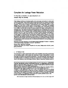
II. P RELIMINARIES A. Conventional FPGA Architecture We assume cluster-based island style FPGA architecture such as that in [23] for all classes of FPGAs studied in this paper. A cluster-based logic block (see Figure 1) includes N fully connected Basic Logic Elements (BLEs). Each BLE
includes one K-input lookup table (LUT) and one flip-flop (DFF). The combination of cluster size N and LUT size K is the architectural issue we evaluate in this paper. The logic blocks are surrounded by routing channels consisting of wire segments. The input and output pins of a logic block can be connected to the wire segments in routing channels via a connection block (see Figure 1 (b)). A routing switch block is located at the intersection of a horizontal channel and a vertical channel. Figure 1 (c) shows a subset switch block [26], where the incoming track can be connected to the outgoing tracks with the same track number.1 The connections in a switch block (represented by the dashed lines in Figure 1 (c)) are programmable routing switches. We implement routing switches by tri-state buffers and use two tri-state buffers for each connection so that it can be programmed independently for either direction. We define an interconnect segment as a wire segment driven by a tri-state buffer or a buffer.2 In this paper, we investigate both uniform length-4 interconnect wire segments and mixed-length interconnects. We decide the routing channel width CW in the same way as the architecture study in [23], i.e., CW = 1.2CWmin where CWmin is the minimum channel width required to route the given circuit successfully. connection block
switch block
0123
logic block in1
0 1 2 3
connection block
element. Therefore, it is time-consuming to explore the huge hyper-architecture solution space using methods from [4], [5]. In order to perform device and architecture co-optimization, an accurate yet extremely efficient timing and power evaluation method is required. The first contribution of this work is that we develop a trace-based estimator (called Ptrace) for FPGA power, delay, and area. We profile placed and routed benchmark circuits and collect statistical information (called trace) on switching activity, short circuit power, near-critical path structure, and circuit element utilization rate for a given set of benchmark circuits (MCNC benchmark set in this paper). We show that the trace is independent of device tuning and it can be used to calculate FPGA chip-level performance and power for a number of device designs. Compared to performing placement-and-routing by VPR [23] followed by cycle-accurate simulation (called Psim) from [5], Ptrace has a high fidelity and an average error of 1.3% for energy and of 0.8% for delay. The trace collecting has the same runtime as evaluating FPGA architecture for one combination of Vdd, Vt and sleep transistor size using VPR and Psim. It took one week to collect the trace for the MCNC benchmark set using eight 1.2GHz Intel Xeon servers while all the hyper-architecture evaluation reported in this paper with over hundreds of hyper-architecture combinations took only a few minutes on one server. The second contribution is that we perform the architecture and device co-optimization for conventional FPGAs and FPGAs with power gating capability. We explore different Vdd, Vt, and sleep transistor size combinations in addition to cluster size and LUT size combinations. For comparison, we obtain the baseline FPGA hyper-architecture which uses the VPR architecture model [23] and the same LUT size and cluster size as the commercial FPGAs used by Xilinx Virtex-II [24], and Vdd suggested by ITRS [25], but Vt optimized by our device optimization. Such baseline is significantly better than the ones with no device optimization. Compared to the baseline hyper-architecture, architecture and device co-optimization can reduce energy-delay product (product of energy per clock cycle and critical path delay, in short, ED) by 18.4% and chip area by 23.3%. Furthermore, considering FPGA architecture with power-gating capability, our architecture and device cooptimization reduces ED by 55.0% and chip area by 8.2% compared to the baseline. We also study the impact of utilization rate and interconnect structure. The rest of the paper is organized as follows. Section II presents the background of FPGA architecture and existing FPGA architecture evaluation flow. Section III introduces our trace-based estimation models. Section IV applies the new estimation models to architecture and device co-optimization. Section V concludes this paper.
2
SR SR
connection switch
(a) Island style routing architecture
(b) Connection block and connection switch
012 3 0 1 2 3
A
B
SR
C
0 1 2 3
A
B
SR
D 012 3
(c) Switch block
(d) Routing switches
Fig. 1. (a) Island style routing architecture; (b) Connection block; (c) Switch block; (d) Routing switches.
B. Vdd gateable FPGA architecture Power gating can be applied to interconnects and logic blocks to reduce FPGA power. Figure 2 illustrates the circuit design of the Vdd-gateable interconnect switch and logic block from [22]. We insert a PMOS transistor (called a sleep transistor) between the power rail and the buffer (or logic block) to provide the power-gating capability. When a buffer or logic block is not used, the sleep transistor is turned off by 1 Without
2 We
loss of generality, we assume subset switch block in this paper. interchangeably use the terms of switch and buffer/tri-state buffer.
IEEE TRANSACTIONS ON COMPUTER-AIDED DESIGN OF INTEGRATED CIRCUITS AND SYSTEMS, VOL. XX, NO. Y, MONTH YEAR
3
Vdd M2
SR
SR SR
M1 A
BUFF
Logic block B
Vdd
in1
Connection switches
Switch
Switch SR
SR
dN dN
Switch
d1
N switches
Switch
SR
Switch
SR
d1
Decoder
(a) Vdd−gateable switch
log2 N SRAM cells
Sram
Logic block
wire track
SR Dec_Disable
(b) Vdd−gateable routing switches Fig. 2.
(c) Vdd−gateable connection block
(d) Vdd gateable logic block
(a) Vdd-gateable switch; (b) Vdd-gateable routing switch; (c) Vdd-gateable connection block; (d) Vdd-gateable logic block.
the configuration cell. SPICE simulation shows that powergating can reduce the leakage power of an unused buffer or a logic block by a factor of over 300. There is power and delay overhead associated with the sleep transistor insertion. The dynamic power overhead is almost negligible. This is due to the fact that the sleep transistors stay either ON or OFF after configuration and there is no charging and discharging at their source/drain capacitors. The delay overhead associated with the sleep transistor insertion can be bounded when the sleep transistor is properly sized. Moreover, the connection box with power gating is different from that in the conventional architecture. For the conventional FPGA, an input MUX, which is effectively an implicit decoder [23], is used in the connection box as illustrated in Figure 1(b). However, for the power gating architecture, an explicit decoder is used in the connection box to enable both the signal path and power supply for the single input, as illustrated in Figure 2(c) [22]. Because the decoder is no longer in the critical path, the delay of connection box in Figure 2(c) is smaller than that in Figure 1(b). The connection box in Figure 2(c) also has a much smaller leakage power but a larger area and a slightly larger dynamic power compared to the conventional architecture. C. FPGA Architecture Evaluation Flow The existing FPGA architecture evaluation flow considering area, delay, and power [6] is illustrated in Figure 3. For a given benchmark set, we first optimize the logic then map the circuit to a given LUT size. TV-Pack is used to pack the mapped circuit to a given cluster size. After packing, we place and route the circuit using VPR [23] and obtain the chip level delay and area. Finally, cycle-accurate power simulator [5] (in short Psim) is used to estimate the chip level power consumption. The architecture evaluation flow discussed above is time consuming because we need to place and route every circuit under different architectures and a large number of randomly generated input vectors need to be simulated for each circuit. However, the device and architecture co-optimization requires
Benchmark Logic Optimization(SIS) Tech-Mapping (RASP)
Arch Spec
Timing-Driven Packing (TV-Pack) Placement & Routing (VPR) Area
Parasitic Extraction Cycle-accurate Power Simulator (Psim)
Delay
Power
Fig. 3. Existing FPGA architecture evaluation flow for a given device setting.
the exploration of the following dimensions: cluster size N , LUT size K, supply voltage Vdd, threshold voltage Vt, and sleep transistor size if power gating is applied. The total number of hyper-architecture combinations can be easily over a few hundreds considering the interaction between these dimensions. Therefore, the conventional evaluation flow is not practical for device and architecture co-optimization due to its time inefficiency. In order to perform device and architecture co-optimization, a fast yet accurate FPGA power and delay estimator is required. Such estimator is just the one we are going to introduce in Section III, the trace-based estimator. III. T RACE - BASED E STIMATION In this section, we will introduce the efficient power and delay estimation model, trace-based estimation method (Ptrace). We speculate that during hyper-architecture evaluation, there are the following two classes of information as summarized in Table I. The first class only depends on architecture and is called the trace of the architecture. The second class only depends on device setting and circuit design. The basic idea of Ptrace is as follows: For a given benchmark set, we profile placed and routed benchmark circuits and collect trace information under one device setting and for one FPGA
IEEE TRANSACTIONS ON COMPUTER-AIDED DESIGN OF INTEGRATED CIRCUITS AND SYSTEMS, VOL. XX, NO. Y, MONTH YEAR
architecture. We then obtain chip-level performance and power for a set of device for a given architecture parameter values based on the trace information. Figure 4 illustrates the flow of trace-based evaluation. Trace Collection
Arch Spec
Circuit Level Area, Delay, and Power
Trace-Based Estimation
Chip Level Area, Delay, and Power
Fig. 4. New trace-based evaluation flow. We perform the same flow as Figure 3 under one device setting to collect the trace information.
4
distinguishes different types of used FPGA resources and applies the following formula: X1 2 Psw = Niu · f · Vdd · Cisw (1) 2 i The summation is over different types of circuit elements, i.e., LUTs, buffers, input pins and output pins. For type i circuit elements, Cisw is the average switch capacitance and Niu is the number of used circuit elements, f is the operating frequency. In this paper, we assume that the circuit works at its maximum frequency, i.e., the reciprocal of the near-critical path delay. The switch capacitance is further calculated as: X Cisw = ( Ci,j /Niu ) · Siu j∈Eli
(2)
= Ciu · Siu
A. Trace collection As mentioned before, the trace information only depends on architecture and remains the same when device setting changes. For a given benchmark set and a given FPGA architecture, the trace includes number of used type i circuit elements (Niu ), total number of type i circuit elements (Nit ), average switching activity of used type i circuit elements (Siu ), short circuit power ratio (αsc ), and near-critical path structure (see Table I). Near-critical path structure is the number of each type of circuit elements (Nip ) on the near-critical path. Device parameters include Vdd and Vt , which depend on technology scale, and average leakage power of type i circuit elements (Pis ), average load capacitance of type i circuit elements (Ciu ), and average delay of type i circuit elements (Di ), which depend on circuit design. The device parameters, such as circuit level delay and power, can be collected by SPICE simulation or by measurement. After collecting the trace and device level delay and power, we can perform Ptrace to estimate the chip level delay, power, and area. Below, we will show that the trace information is insensitive to the device parameters and discuss our trace-based models. Trace Parameters (depend on architecture) Niu # of used type i circuit elements t Ni total # of type i circuit elements u Si avg. switching activity for used type i circuit elements p Ni # of type i circuit elements on the near-critical path αsc ratio between short circuit power and switch power Device Parameters (depend on processing technology and circuit design) V dd power supply voltage Vt threshold voltage s Pi avg. leakage power for type i circuit elements u Ci avg. load capacitance of type i circuit elements Di avg. delay of type i circuit elements
TABLE I T RACE INFORMATION , DEVICE AND
CIRCUIT PARAMETERS .
B. Dynamic Power Model Dynamic power includes switch power and short-circuit power. A circuit implemented on an FPGA cannot utilize all circuit elements. Dynamic power is only consumed by the used FPGA resources. Our trace-based switch power model
For type i circuit elements, Ciu is the average load capacitance of used circuit elements, which is averaged over Ci,j , the local load capacitance for used circuit element j. Eli is the set of used type i circuit elements, and Siu is the average switching activity of used type i circuit elements. We assume that the average switching activity of the circuit elements is determined by the circuit logic functionality and FPGA architecture. The device parameters of Vdd and Vt have a limited effect on switching activity. We verify this assumption in Table II by demonstrating the average switching activity of five benchmarks at different technology nodes, and Vdd and Vt levels. benchmark
alu4 apex2 apex4 bigkey clma
70nm Vdd=1.1 Vt=0.25 logic interconnect 2.06 0.55 1.73 0.47 1.23 0.27 1.75 0.56 0.90 0.21
100nm Vdd=1.3 Vt=0.32 logic interconnect 2.01 0.54 1.75 0.47 1.19 0.26 1.96 0.59 0.87 0.21
70nm Vdd=1.0 Vt=0.20 logic interconnect 2.03 0.59 1.70 0.47 1.16 0.29 1.71 0.55 0.91 0.23
TABLE II SWITCHING ACTIVITIES FOR DIFFERENT TECHNOLOGY NODES ,
V DD AND
V T. A RCHITECTURE SETTING : N = 10, K = 4. U NIT: SWITCH PER CLOCK CYCLE .
The short circuit power is related to signal transition time, which is difficult to obtain without detailed simulation using a real delay model. In our trace-based model, we model the short circuit power as: Psc = Psw · αsc
(3)
Where αsc is the ratio between short circuit power and switch power. Although this ratio value at the circuit level depends on FPGA circuit design and architecture, we assume that αsc does not depend on device and technology at the chip level. We verify this assumption in Table III3 by showing the average short circuit power ratio at different technology nodes, Vdd, and Vt levels. 3 Because the delay between buffers is usually large for FPGA circuits, the short circuit power ratio could be big.
IEEE TRANSACTIONS ON COMPUTER-AIDED DESIGN OF INTEGRATED CIRCUITS AND SYSTEMS, VOL. XX, NO. Y, MONTH YEAR benchmark
alu4 apex2 apex4 bigkey clma
70nm Vdd=1.1 Vt=0.25 logic interconnect 1.43 1.12 1.44 0.89 1.08 0.86 0.74 1.64 1.11 1.72
100nm Vdd=1.3 Vt=0.32 logic interconnect 1.44 1.16 1.42 0.93 1.15 0.79 0.76 1.71 1.21 1.62
70nm Vdd=1.0 Vt=0.20 logic interconnect 1.46 1.15 1.48 0.92 1.18 0.82 0.72 1.68 1.16 1.63
For resource type i, Nip is the number of circuit elements that the near-critical path goes through, and Di is the delay of such a circuit element. Di is a circuit parameter depending on Vdd, Vt, process technology, and FPGA architecture.5 To get the path statistical information Nip , we only need to place and route the circuit once for a given FPGA architecture.
TABLE III S HORT CIRCUIT POWER RATIOS FOR DIFFERENT TECHNOLOGY NODES , V DD AND V T. A RCHITECTURE SETTING : N = 10, K = 4.
C. Leakage Power Model The leakage power is modeled as follows, X Nit Pis Pstatic =
(4)
i
For resource type i, Nit is the total number of circuit elements, and Pis is the leakage power for a type i element. Notice that usually Nit > Niu because the resource utilization rate is low in FPGAs (typically 62.5% [1]). For an FPGA architecture with power-gating capability, an unused circuit element can be power-gated to reduce leakage power.4 In this case, the total leakage power is modeled by the following formula: X X (Nit − Niu )Pi (5) Niu Pi + αgating · Pstatic = i
i
5
where αgating is the average leakage ratio between a powergated circuit element and a circuit element in normal operation. SPICE simulation shows that sleep transistors can reduce leakage power by a factor of 300 and αgating = 0.003 is used in this paper.
E. Validation of Ptrace To validate Ptrace, we compare it to the conventional architecture evaluation flow for ITRS [25] 70nm technologies. We assume Vdd=1.0V and Vt=0.2V and map 20 MCNC benchmarks, as illustrated in Table IV, to two architectures: {N = 8, K = 4} and {N = 6, K = 7}. In Table IV, the number of LUTs and flip flops are counted under the architecture N=8 and K=4. Notice that we can map the benchmarks to different LUT and cluster sizes. We collect trace using the conventional architecture evaluation flow in 70nm technology, Vdd=1.0V and Vt=0.2V. Figure 5 compares energy and delay between the conventional evaluation flow and Ptrace for each benchmark. The average energy error of Ptrace is 1.3% and average delay error is 0.8%. From the figure, the Ptrace has the same trends for energy as Psim does and for delay as VPR does. Therefore, Ptrace has a high fidelity. Moreover, the run time of Ptrace is 2s, while that of the conventional evaluation flow is 120 hours. benchmark alu4 apex2 apex4 bigkey clma des diffeq dsip elliptic ex1010
# LUTs 1607 2118 1291 2935 13537 2172 1933 1619 4185 4721
D. Delay Model To avoid the static timing analysis for the entire circuit implemented on a given FPGA fabric, we obtain the structure of the ten longest circuit paths including the near-critical path for each circuit. The path structure is the number of elements of different resource types, i.e., LUT, wire segment and interconnect switch, on one circuit path. We assume that the new near-critical path due to different Vdd and Vt levels is among these ten longest paths found by our benchmark profiling. When Vdd and Vt change, we can calculate delay values for the ten longest paths under new Vdd and Vt levels, and choose the largest one as the new near-critical path delay. Therefore, the FPGA delay can be calculated as follows: X p D= Ni D i (6) i 4 In this paper, we assume the wire segment length change introduced by power √gating can be ignored. In our experiment, wire length is calculated as 4 × areatile [23], where areatile is the area of a logic block with the interconnect surrounding it. The area overhead introduced by power gating is less than 30%. Therefore, the change of wire segment length is less than 14%. Moreover the load capacitance of a routing buffer is mainly determined by the input and output capacitances of buffers. The wire capacitance is a small portion (about 20%) of the load capacitance. Therefore, the area increase introduced by power gating will have small impact on the delay and power estimation.
# Flip flops 0 0 0 224 33 0 377 224 1138 0
benchmark ex5p frisc misex3 pdc s298 s38417 s38584 seq spla tseng
# LUTs 1201 5926 1501 5608 2548 8458 7040 1953 3938 1299
# Flip flops 0 900 0 0 8 1463 1260 0 0 382
TABLE IV MCNC BENCHMARK LIST. T HE NUMBER OF LUT S AND
FLIP FLOPS ARE
COUNTED UNDER THE ARCHITECTURE N=8 AND
IV.
HYPER - ARCHITECTURE
K=4.
E VALUATION
A. Overview In this section, we use Ptrace to perform device and architecture evaluation. We consider 70nm ITRS technology and evaluate four FPGA hyper-architecture classes: HomoVt, Hetero-Vt, Homo-Vt+G and Hetero-Vt+G. Homo-Vt is the conventional FPGA using homogeneous Vt for interconnects and logic blocks. Hetero-Vt applies different Vt to logic blocks and interconnects. Homo-Vt+G and Hetero-Vt+G are the same as Homo-Vt and Hetero-Vt, respectively, except that unused logic blocks and interconnects are power-gated [22]. We compare them with the baseline hyper-architecture, which 5 Delay of each circuit element is measured with the worst case switch. When power gating is applied, a single gating transistor is used for the entire logic block. In order to measure the delay of each circuit element in a logic block with gating transistor, a series of randomly generated vectors are used as the inputs to the block and the worst case delay is measured for each circuit element under such random input vectors.
IEEE TRANSACTIONS ON COMPUTER-AIDED DESIGN OF INTEGRATED CIRCUITS AND SYSTEMS, VOL. XX, NO. Y, MONTH YEAR
Delay from Ptrace(ns)
45
8x4 6x7
36 27
4% Error 18 9 0
0
9
18 27 36 Delay from VPR(ns)
45
Energy from Ptrace (nJ)
10
8x4 6x7
8
6
will be discussed in subsections IV-E and IV-F, respectively. For each hyper-architecture, we compute the energy, delay and area as the geometric mean of 20 MCNC benchmarks in Table IV. Moreover, in the rest of this paper, we use CVt for Vt of logic blocks and IVt for Vt for global interconnects. Note that CVt=IVt in Homo-Vt and Homo-Vt+G. To illustrate the tradeoff between energy and delay, we introduce the concept of dominant hyper-architecture: If hyper-architecture A has less energy consumption and a smaller delay than hyperarchitecture B, then we say that B is inferior to A. We define the dominant hyper-architectures as the set of hyper-architectures that are not inferior to any other hyper-architectures. We organize the rest of this section as follows: First, Section IV-B illustrates the necessity of device and architecture co-optimization. Then Section IV-C presents the energy and delay tradeoff and ED reduction achieved by device and architecture co-optimization. Section IV-D discusses the device and architecture co-optimization considering area. Finally, Sections IV-E and IV-F analyze the impact of utilization rate and compare the evaluation result of different routing architectures, respectively. Baseline FPGA device/arch parameter values Vdd Vt N K 0.9v 0.3v 8 4 Value range for device/arch optimization Vdd Vt N K 0.8v-1.1v 0.2v-0.4v 6-12 3-7
6
5% Error 4
TABLE V B ASELINE HYPER - ARCHITECTURE AND EVALUATION RANGES .
2 0 0
Fig. 5.
2
4 6 8 Energy from Psim (nJ)
10
Comparison between Psim and Ptrace
uses the VPR architecture model [23] and has the same LUT size and cluster size as those used by the Xilinx Virtex-II [24] (cluster size of 8, LUT size of 4), Vdd suggested by ITRS [25] (0.9v), and Vt of 0.3v that is optimized with respect to the above architecture and Vdd. The baseline hyper-architecture and evaluation ranges for device and architecture are presented in Table V. Note that a high Vt is applied to all SRAM cells for configuration to reduce their leakage power as suggested by [12]. In the subsections IV-B to IV-D, we assume the following: •
•
•
•
The utilization rate (defined as the utilization rate of logic blocks, i.e., number of used logic blocks over the number of total available logic blocks) is 0.5. All interconnect wire segments span 4 logic blocks with fully buffered routing switches. The routing channel width is 1.2 times of the minimum channel width that allows the FPGA circuit being routed. All benchmark circuits work at their highest frequency (1/critical path delay).
The impact of utilization rate and interconnect architecture
B. Necessity of device and architecture co-optimization In this section, we show the necessity of device and architecture co-optimization. We first discuss the need of device tuning, then compare the results of optimizing device and architecture separately and simultaneously. Architecture evaluation has been studied in previous research [4], [5], [21], [22], [27], [28]. However, device tuning has not been reported in the literature. Our experiments show that device tuning has a much greater impact on delay and energy than architecture tuning does, which is demonstrated in Figure 6 and Table VI. Each set of data points in Figure 6 is the dominant hyper-architectures for a given device setting. 6 For example, set D4 is the dominant hyper-architectures under Vdd=1.0V and Vt=0.25V. From the figure, we observe that a change on the device leads to a more significant change in energy and delay than architecture change does. For example, for device setting Vdd = 0.9V and Vt=0.25v, energy for different architectures ranges from 1.82nJ to 2.11nJ, and delay ranges from 13.68ns to 16.46ns. However, if we increase Vt by 0.05v, i.e., Vdd = 0.9V and Vt = 0.3V , the energy ranges from 1.17nJ to 1.32nJ and the delay ranges from 18.99ns to 23.24ns. Therefore, it is important to evaluate both device and architecture instead of evaluating architecture only. 6 Dominant hyper-architectures for a given device setting are the hyperarchitectures that are not inferior to any other hyper-architectures under such device setting.
IEEE TRANSACTIONS ON COMPUTER-AIDED DESIGN OF INTEGRATED CIRCUITS AND SYSTEMS, VOL. XX, NO. Y, MONTH YEAR
is also small (only 34.1s). Therefore, it is still worthwhile performing simultaneous device and architecture optimization.
18 D1 Vdd 0.9 Vt 0.25 D2 Vdd 0.9 Vt 0.30 D3 Vdd 0.9 Vt 0.35 D4 Vdd 1.0 Vt 0.25 D5 Vdd 1.0 Vt 0.30 D6 Vdd 1.0 Vt 0.35 D7 Vdd 1.1 Vt 0.25 D8 Vdd 1.1 Vt 0.30 D9 Vdd 1.1 Vt 0.35
16
Energy per cycle (nJ)
14
D7
12 10 8
D8
6 D9
4 2
D4
D1 D5
0 10 Fig. 6. Set D1 D2 D3 D4 D5 D6 D7 D8 D9
15
D6
C. Energy and delay tradeoff
D3
D2 20
25 Delay (ns)
30
35
40
hyper-architectures under different device settings. Vdd (V) 0.9 0.9 0.9 1.0 1.0 1.0 1.1 1.1 1.1
Vt (V) 0.25 0.30 0.35 0.25 0.30 0.35 0.25 0.30 0.35
Min energy (nJ) 1.82 1.17 0.97 2.30 1.37 1.11 5.58 3.10 1.95
Max energy (nJ) 2.11 1.32 1.05 3.17 1.95 1.30 17.01 9.03 4.73
Min delay (ns) 13.68 18.99 31.01 11.90 15.60 21.31 10.60 13.05 17.01
Max delay (ns) 16.46 23.24 36.40 14.06 17.50 24.66 12.43 15.40 19.92
TABLE VI P OWER AND
7
DELAY RANGES FOR DIFFERENT DEVICE SETTINGS .
There are three methods to perform device and architecture optimization. In the first method, we first optimize device using one architecture then optimize the architecture under the optimized device setting and call it device-arch method. In the second method, we first optimize the architecture within one device setting then optimize the device setting according to the optimized architecture and call it arch-device method. In the third method, we optimize architecture and device simultaneously and call it simultaneous method. Both methods arch-device and device-arch cannot guarantee the optimal solution. Table VII compares the min-ED hyper-architectures for Homo-Vt found by three different methods. For both archdevice and device-arch, we start search from the baseline case {N = 8, K = 4, Vdd = 0.9V , and Vt = 0.3V }. In our experiment, we find that there are two local optimal hyper-architectures in the whole solution space: {N = 6, K = 7, Vdd = 0.9V , Vt = 0.3V } and {N = 10, K = 4, Vdd = 1.0V , Vt = 0.3V } which is also the global optimal. In this particular example, both arch-device and device-arch achieve the same local optimal hyper-architecture {N = 6, K = 7, Vdd = 0.9V , Vt = 0.3V }. If we start search from some other hyper-architectures, arch-device and device-arch may achieve other local optimum but there is no guarantee of the global optimum. In order to obtain the global optimal solution, we have to use the simultaneous method. From Table VII, we observe that simultaneous method can reduce ED by 13.3% compared to arch-device and device-arch. We also see that the runtime of arch-device and device-arch is shorter than that of simultaneous method. However, due to the time efficiency of Ptrace, the runtime of simultaneous method
In this section, we first compare the impact of device tuning and architecture tuning, then present min-energy and min-delay hyper-architectures, and finally discuss the energy and delay tradeoff. For the classes Homo-Vt+G and HeteroVt+G with power-gating, we assume the following fixed sleep transistor size: 210X PMOS for a logic block, 10X PMOS for a switch buffer, and 1X PMOS for a connection buffer. We then discuss the sleep transistor tuning in Section IV-D. Table VIII summarizes the minimum delay and minimum energy hyper-architectures for each class. The minimum delay hyper-architectures have cluster size of 6 and LUT size of 7 which are the same for all classes. The minimum energy hyper-architectures have LUT size of 4 for all classes. This is similar to the previous evaluation result [5], [22]. As expected, the min-delay hyper-architectures have the highest Vdd and lowest Vt. However, the min-energy hyper-architectures have the lowest Vdd but not the highest Vt. This is because we assume that each circuit works at its highest possible frequency (1/critical path delay). The energy is calculated as E = delay · power. When Vt is too high, the delay is so large that the energy per clock cycle increases. Usually, higher performance hyper-architectures consume more energy. To illustrate the energy and delay tradeoff, we present the dominant hyper-architectures of Homo-Vt and Hetero-Vt in Figure 7 (a) and those of Homo-Vt+G and Hetero-Vt+G in Figure 7 (b). From the figure, we find that the energy difference between Homo-Vt+G and Hetero-Vt+G is smaller than that between Homo-Vt and Hetero-Vt. This is because leakage power is significantly reduced by power-gating and therefore more detailed Vt tuning such as heterogeneousVt has a smaller impact. We also see that dominant hyperarchitectures of Homo-Vt+G and Hetero-Vt+G have smaller delay than that of Homo-Vt and Hetero-Vt. This is due to the fact that the connection box with power gating has smaller delay than that without power gating as discussed in Section II-B. Moreover, with the dominant hyper-architecture figure, we can obtain the minimum energy solution for a given performance range. For example, if we want to find the minimum energy solution for Homo-Vt with delay limit 15ns, we only need to pick the dominant hyper-architecture whose delay is closest to 15ns. In order to achieve the best energy and delay tradeoff, we find the hyper-architectures with the minimum energy delay product (in short min-ED) in Table IX. Compared to the baseline, ED reduction is 14.5% and 18.4% for Homo-Vt and Hetero-Vt, respectively. If power gating is applied, ED can be reduced by about 60% for both Homo-Vt+G and Hetero-Vt+G. The similar ED reduction for power gating classes is due to the fact that leakage power is greatly reduced by power-gating and therefore the more detailed Vt tuning such as heterogeneousVt has a small impact on power reduction as discussed before. We also see that, compared to the min-ED hyper-architectures without power gating, the min-ED hyper-architectures with
IEEE TRANSACTIONS ON COMPUTER-AIDED DESIGN OF INTEGRATED CIRCUITS AND SYSTEMS, VOL. XX, NO. Y, MONTH YEAR Vdd (V) 0.9 0.9 1.0
arch-device device-arch simultaneous
CVt (V) 0.30 0.30 0.30
IVt (V) 0.30 0.30 0.30
(N, k) (6,7) (6,7) (10,4)
Energy (nJ) 1.38 1.38 1.37
Delay (ns) 19.8 19.8 17.5
ED (nJ· ns) 27.3 27.3 24.1 (-13.3%)
8
runtime (s) 5.1 3.4 34.1
TABLE VII M IN -ED HYPER - ARCHITECTURE OF OPTIMIZING DEVICE AND ARCHITECTURE SEPARATELY AND SIMULTANEOUSLY.
hyper-architecture Class Homo-Vt Hetero-Vt Homo-Vt+G Hetero-Vt+G
Vdd(V) 1.1 1.1 1.1 1.1
Minimum delay CVt(V) Ivt(V) 0.20 0.20 0.20 0.20 0.20 0.20 0.20 0.20
hyper-architecture (N,K) Energy(nJ) (6,7) 31.22 (6,7) 31.22 (6,7) 15.98 (6,7) 15.98
Delay(ns) 8.86 8.86 9.45 9.45
Vdd(V) 0.8 0.8 0.8 0.8
Minimum energy hyper-architecture CVt(V) Ivt(V) (N,K) Energy(nJ) 0.35 0.35 (10,4) 0.942 0.30 0.35 (12,4) 0.920 0.30 0.30 (12,4) 0.550 0.30 0.25 (10,4) 0.549
Delay(ns) 59.2 43.6 30.5 24.3
TABLE VIII M INIMUM DELAY
AND MINIMUM ENERGY HYPER - ARCHITECTURES .
D. ED and area tradeoff
tradeoff for FPGA architecture. Usually, the larger the sleep transistor size, the smaller the delay is. In this section, we perform device and architecture co-optimization to achieve the best ED and area tradeoff. Although dual-Vt may change the layout area due to extra diffusion well area, such change depends on technology and is often very small. Therefore, in this section, we assume that Vdd and Vt change does not affect area. For Homo-Vt and Hetero-Vt, because no power gating is applied, we do not need to tune sleep transistor size. To achieve the best ED-area tradeoff, we find out the hyper-architectures with minimum product of energy, delay, and area (in short AED), which are summarized in Table X. Compared to the baseline, the min-AED hyper-architecture of Homo-Vt reduces ED by 14.7% and area by 18.3%,7 and the min-AED hyperarchitecture of Hetero-Vt reduces ED by 18.4% and area by 23.3%. Figure 8 presents the chip-level ED and area tradeoff. We prune inferior solutions with both ED and area larger than any alternative solutions. From the figure, we see that, for the classes without power gating, the min-ED hyper-architecture is exactly the min-AED hyper-architecture. This is because that when no power gating is applied, the larger the area, the more leakage power is consumed. Therefore, the min-ED hyperarchitectures use less area than other hyper-architectures. For Homo-Vt+G and Hetero-Vt+G with power gating, the sleep transistor size has to be considered. Because only one sleep transistor is used for one logic block, as illustrated in Figure 2(d), we assume the 210X PMOS for the sleep transistor with negligible area overhead. Moreover, we observe that a 1X PMOS as the sleep transistor for one switch in connection box (see the circuit in Figure 2(c)) provides good performance, and any further increase of the sleep transistor size cannot improve the performance much. The sleep transistors for the switches in the routing box, however, may affect delay greatly. We consider four sleep transistor sizes: 2X, 4X, 7X, and 10X PMOS for a routing switch. From the Figure 8, we find that device and architecture
In the previous sections, we assume fixed sleep transistor sizes for Homo-Vt and Hetero-Vt+G and discuss hyperarchitecture evaluation to minimize ED without considering area. However, area is important for FPGA design. Powergating using sleep transistors may change delay and area
7 In our evluation, we assume that the area depends only on architecture and but not device setting. Our experimental result shows that N = 12, K = 4 is most area efficient architecture, this architecture reduces area by 23.6% compared to the baseline (N = 8, K = 4). The architecture N = 10, K = 4 is the second area efficient architecture which reduces area by 18.3% compared to the baseline.
Energy per cycle (nJ)
32
Min delay hyper-arch for Homo-Vt
24
Homo-Vt Hetero-Vt
Min-ED hyper-arch for Homo-Vt
16
Min-ED Min energy hyper-arch hyper-arch for Hetero-Vt for Hetero-Vt
8
Min energy hyper-arch for Homo-Vt
0 8
21
34 (a) Delay (ns)
47
60
Energy per cycle (nJ)
18 Homo-Vt+G Hetero-Vt+G
Min delay hyperarch for HomoVt+G and Hetero-
15 12
Min-ED hyper-arch for Homo-Vt+G Min-ED hyper-arch for Hetero-
9 6
Min energy hyper-arch for ㋏߫5 Homo-Vt ㋏߫6 Min energy ㋏߫7 hyper-arch for Hetero-Vt+G
3 0 8
13
18 23 (b) Delay (ns)
28
33
Fig. 7. Dominant hyper-architectures. (a) Homo-Vt and Hetero-Vt (b) HomoVt+G and Hetero-Vt+G
power gating has a lower Vt. This is because leakage power is greatly reduced when power gating is applied, therefore a lower Vt can improve performance without much penalty on leakage.
IEEE TRANSACTIONS ON COMPUTER-AIDED DESIGN OF INTEGRATED CIRCUITS AND SYSTEMS, VOL. XX, NO. Y, MONTH YEAR hyper-architecture.Class Baseline Homo-Vt Hetero-Vt Homo-Vt+G Hetero-Vt+G
Vdd (V) 0.9 1.0 0.9 0.9 0.8
CVt (V) 0.30 0.30 0.25 0.25 0.25
IVt (V) 0.30 0.30 0.30 0.25 0.20
(N, k) (8,4) (10,4) (12,4) (12,4) (10,4)
Energy (nJ) 1.20 1.37 1.27 0.74 0.65
Delay (ns) 23.5 17.5 18.1 16.10 17.30
ED (nJ· ns) 28.2 24.1 23.0 11.9 11.2
9
ED Reduction % 14.5 18.4 57.8 60.3
Normalized Area % 100.00 81.90 79.52 127.43 126.19
TABLE IX C OMPARISON BETWEEN BASELINE AND
Baseline Homo-Vt Hetero-Vt Homo-Vt+G Hetero-Vt+G
Vdd (V) 0.9 1.0 0.9 0.9 0.9
CVt (V) 0.30 0.30 0.25 0.25 0.25
IVt (V) 0.30 0.30 0.30 0.25 0.20
MIN -ED HYPER - ARCHITECTURE IN
(N,K) (8,4) (10,4) (12,4) (12,4) (12,4)
Sleep transistor size 2 2
Homo-Vt, Hetero-Vt, Homo-Vt+G,
Normalized ED 1 0.853 0.816 0.470 0.450
Normalized Area 1 0.817 0.767 0.918 0.918
AND
Hetero-Vt+G.
AED product 0.697 0.626 0.432 0.413
AED reduction % 30.3 37.4 56.9 58.7
TABLE X M INIMUM ED- AREA PRODUCT HYPER - ARCHITECTURES FOR DIFFERENT CLASSES . ED, A REA , AND ED- AREA PRODUCT ARE
NORMALIZED WITH
RESPECT TO THE BASELINE .
Normalized area
1.3
1.1
Min AED hyper-arch for Homo-Vt+G
0.9
Homo-Vt Hetero-Vt Homo-Vt+G Hetero-Vt+G Min AED hyper-arch for Homo-Vt
Min AED hyper-arch for Hetero-Vt
Min AED hyper-arch for Hetero-Vt+G
0.7 0.3
0.4
0.5
0.6 0.7 0.8 Normalized ED
0.9
1.0
Fig. 8. ED and area trade-off. ED and area are normalized with respect to the baseline (N = 8, K = 4, Vdd = 0.9V , and Vt = 0.3V ).
co-optimization can reduce ED and area simultaneously even when power gating is applied. This is due to the fact that tuning device setting and architecture offers a bigger solution space to explore in chip level. 8 Table X summarizes the minimum AED product hyper-architectures. Compared to the baseline case, the minimum AED product hyper-architecture of Homo-Vt+G reduces ED by 53.0% and area by 8.2% and the minimum AED product hyper-architecture in Hetero-Vt+G reduces ED by 55.0% and area by 8.2%. E. Impact of utilization rate In the previous part of this section, we assume fixed utilization rate (0.5). In this subsection, we will further discuss the impact of utilization rate on FPGA architecture evaluation. We compare the min-ED and min-AED hyper-architectures under three different utilization rates: 0.3, 0.5, and 0.8 in Tables XI and XII. We see that the min-ED and min-AED hyperarchitectures under different utilization rates are the same. 8 As discussed before, the most area efficient architectures (N = 12 and K = 4) reduces area by about 20% compared to the baseline. The area increase introduced by power gating leads to only about 15% area increase. Therefore, for the minimum AED hyper-architecture of the power gating classes consumes less area compared to the baseline.
Therefore, we conclude that utilization rate in practice does not affect hyper-architecture evaluation. We guess that the reason why the utilization rate does not affect hyper-architecture evaluation is as follows: In our models the performance and dynamic power of the circuit under different utilization rates are the same, 9 and the only difference is leakage power. For the classes with power gating, the leakage power is determined by the active elements and the leakage power of the unused circuit elements is negligible (as we can see from Table XI, in classes Homo-Vt+G and Hetero-Vt+G, ED under different utilization rate is very close). When no power gating is applied, for given benchmark circuits, leakage power is the dominant power component and changes inversely proportional to the utilization rate. Therefore the relationship between the leakage power of different hyper-architectures does not change with respect to the change of the utilization rate. F. Impact of interconnect structure In the previous discussion, we always assume all the wire segments span four logic blocks (i.e. length-4 interconnect wires). In this section, we will compare two routing structures to show the impact of routing structure on delay and power. We compare a structure with uniform length-4 wire segments (in short uniform-interconnect) and a routing structure with 60% length-4 wire segments and 40% length-8 wire segments (in short mixed-interconnect). The mixed-interconnect is optimal for minimizing delay [29]. Tables XIII, XIV, and XV compare the min delay, min energy and min ED hyper-architectures between the two routing structures, respectively. We see that the min-delay hyper-architectures for both interconnect structures are same. The min-energy and min-ED hyper-architectures for the two routing structure have the same the device setting and LUT size, but mixed-interconnect tends to use smaller cluster size as the interconnect delay is reduced in mixed-interconnect. We also see that uniform-interconnect has lower energy but higher delay than mixed-interconnect. This is due to the fact that mixed-interconnect applies length-8 wire-segments and 9 We assume the placement and route is the same for different utilization rate.
IEEE TRANSACTIONS ON COMPUTER-AIDED DESIGN OF INTEGRATED CIRCUITS AND SYSTEMS, VOL. XX, NO. Y, MONTH YEAR Utilization rate Homo-Vt Hetero-Vt Homo-Vt+G Hetero-Vt+G
Vdd (V) 1.0 0.9 0.9 0.8
CVt (V) 0.30 0.25 0.25 0.25
0.3 IVt (V) 0.30 0.30 0.25 0.20
(N, k) (10,4) (12,4) (12,4) (10,4)
ED (nJ· ns) 32.0 31.5 12.3 11.6
Vdd (V) 1.0 0.9 0.9 0.8
CVt (V) 0.30 0.25 0.25 0.25
0.5 IVt (V) 0.30 0.30 0.25 0.20
(N, k)
ED (nJ· ns) 24.1 23.0 11.9 11.2
(10,4) (12,4) (12,4) (10,4)
Vdd (V) 1.0 0.9 0.9 0.8
CVt (V) 0.30 0.25 0.25 0.25
0.8 IVt (V) 0.30 0.30 0.25 0.20
10
(N, k) (10,4) (12,4) (12,4) (10,4)
ED (nJ· ns) 19.4 18.1 11.8 11.0
TABLE XI M IN -ED HYPER - ARCHITECTURE UNDER DIFFERENT UTILIZATION RATES .
Utilization rate Homo-Vt Hetero-Vt Homo-Vt+G Hetero-Vt+G
Vdd (V) 1.0 0.9 0.9 0.8
CVt (V) 0.30 0.25 0.25 0.25
IVt (V) 0.30 0.30 0.25 0.20
0.3 (N, k) (10,4) (12,4) (12,4) (10,4)
Sleep Tran 2 2
AED 0.649 0.637 0.330 0.324
Vdd (V) 1.0 0.9 0.9 0.8
CVt (V) 0.30 0.25 0.25 0.25
IVt (V) 0.30 0.30 0.25 0.20
0.5 (N, k) (10,4) (12,4) (12,4) (10,4)
Sleep Tran 2 2
AED 0.697 0.626 0.432 0.413
Vdd (V) 1.0 0.9 0.9 0.8
CVt (V) 0.30 0.25 0.25 0.25
0.8 (N, k)
IVt (V) 0.30 0.30 0.25 0.20
(10,4) (12,4) (12,4) (10,4)
TABLE XII M IN -AED HYPER - ARCHITECTURE UNDER DIFFERENT UTILIZATION RATES . N OTE : AED IS NORMALIZED WITH RESPECT TO
therefore a buffer with a larger size is used, which reduces delay but increases power. hyper-architecture Class Homo-Vt Hetero-Vt Homo-Vt+G Hetero-Vt+G
Vdd (V) 1.1 1.1 1.1 1.1
Homo-Vt Hetero-Vt Homo-Vt+G Hetero-Vt+G
1.1 1.1 1.1 1.1
uniform-interconnect CVt Ivt (N,K) (V) (V) 0.20 0.20 (6,7) 0.20 0.20 (6,7) 0.20 0.20 (6,7) 0.20 0.20 (6,7) mixed-interconnect 0.20 0.20 (6,7) 0.20 0.20 (6,7) 0.20 0.20 (6,7) 0.20 0.20 (6,7)
Energy (nJ) 31.22 31.22 15.98 15.98
Delay (ns) 8.86 8.86 9.45 9.45
35.56 35.56 16.25 16.25
8.42 8.42 9.13 9.13
hyper-architecture Class Homo-Vt Hetero-Vt Homo-Vt+G Hetero-Vt+G
Vdd (V) 1.0 0.9 0.9 0.8
Homo-Vt Hetero-Vt Homo-Vt+G Hetero-Vt+G
1.0 0.9 0.9 0.8
uniform interconnect CVt Ivt (N,K) (V) (V) 0.30 0.30 (10,4) 0.25 0.30 (12,4) 0.25 0.25 (12,4) 0.25 0.20 (10,4) mixed-interconnect 0.30 0.30 (8,4) 0.25 0.30 (12,4) 0.25 0.25 (8,4) 0.25 0.20 (8,4)
Sleep Tran 2 2
AED 0.698 0.617 0.533 0.510
THE BASELINE .
Energy (nJ) 1.37 1.27 0.74 0.65
Delay (ns) 17.50 18.10 16.10 17.30
ED (nJ·ns) 24.1 23.0 11.9 11.2
1.51 1.39 0.82 0.74
17.00 18.40 16.40 16.67
25.7 25.6 13.4 12.3
TABLE XV M IN -ED HYPER - ARCHITECTURE UNDER DIFFERENT ROUTING STRUCTURES .
TABLE XIII M IN - DELAY HYPER - ARCHITECTURE UNDER DIFFERENT ROUTING STRUCTURES .
hyper-architecture Class Homo-Vt Hetero-Vt Homo-Vt+G Hetero-Vt+G
Vdd (V) 0.8 0.8 0.8 0.8
Homo-Vt Hetero-Vt Homo-Vt+G Hetero-Vt+G
0.8 0.8 0.8 0.8
uniform-interconnect CVt Ivt (N,K) (V) (V) 0.35 0.35 (10,4) 0.30 0.35 (12,4) 0.30 0.30 (12,4) 0.30 0.25 (10,4) mixed-interconnect 0.35 0.35 (8,4) 0.35 0.35 (8,4) 0.30 0.30 (12,4) 0.30 0.25 (8,4)
Energy (nJ) 0.942 0.920 0.550 0.549
Delay (ns) 59.2 43.6 30.5 24.3
1.052 1.052 0.610 0.602
55.6 55.6 29.3 22.8
TABLE XIV M IN - ENERGY HYPER - ARCHITECTURE UNDER DIFFERENT ROUTING STRUCTURES .
V. C ONCLUSIONS
AND
D ISCUSSIONS
In this paper, we have developed trace-based power and performance evaluation (Ptrace) for FPGA. The one-time use of placement, routing and cycle-accurate power simulation is applied to collect the timing and power trace for a given benchmark set and a given FPGA architecture. The trace can then be re-used to calculate timing and power via closedform formulae for different device parameters and technology
scaling. Ptrace is much faster, yet accurate compared to the conventional evaluation based on placement and routing by VPR [23] followed by cycle-accurate simulation (Psim) [5]. Using the trace-based estimation, we have performed device (Vdd, Vt and sleep transistor size if power gating is applied) and architecture (cluster and LUT size) co-optimizations for low power FPGAs. We assume the ITRS [25] 70nm technology and use the following baseline for comparison: Cluster size of 8 and LUT size of 4 as in the Xilinx Virtex-II [24], Vdd of 0.9v suggested by ITRS, Vt of 0.3v which is optimized for min-ED (i.e., minimum energy delay product) with respect to the above architecture and Vdd. Compared to the baseline case, simultaneous optimization of FPGA architecture and device reduces the min-ED by 14.7% and area by 18.3% for FPGA using homogeneous-Vt for the logic blocks and interconnects without power gating. Optimizing Vt separately (i.e., heterogeneous-Vt) for the logic block and interconnect reduces min-ED by 18.4% and area by 23.3%. Furthermore, power gating unused logic and interconnect reduces the minED by up to 55.0% and reduces area by 8.2%. Compared to the classes without power gating, the min-ED hyper-architectures of the classes with power gating have lower Vt. This is due to the fact that, when power gating is applied, leakage power is significantly reduced and therefore a lower Vt can be applied to reduce delay. We observe that min-ED hyper-architectures and min-AED
IEEE TRANSACTIONS ON COMPUTER-AIDED DESIGN OF INTEGRATED CIRCUITS AND SYSTEMS, VOL. XX, NO. Y, MONTH YEAR
hyper-architectures for different utilization rates (between 30% and 80%) are the same. Therefore, the utilization rate in practice does not affect the device and architecture co-optimization result. Moreover, we also test two different routing structures, one with uniform length 4 wire segments (uniforminterconnect) and the other with 60% length 4 wire segments and 40% length 8 wire segments (mixed-interconnect). We observe that the min-ED, min-energy and min-delay hyperarchitectures under two different interconnect structures are similar, except that mix-interconnect tends to use slightly smaller cluster size due to the reduced interconnect delay. R EFERENCES [1] T. Tuan and B. Lai, “Leakage power analysis of a 90nm FPGA,” in Proc. IEEE Custom Integrated Circuits Conf., 2003. [2] E. Kusse and J. Rabaey, “Low-energy embedded FPGA structures,” in Proc. Intl. Symp. Low Power Electronics and Design, pp. 155–160, August 1998. [3] V. Degalahal and T. Tuan, “Methodology for high level estimation of FPGA power consumption,” in Proc. Asia South Pacific Design Automation Conf., Jan 2005. [4] K. Poon, A. Yan, and S. Wilton, “A flexible power model for FPGAs,” in Proc. of 12th International conference on Field-Programmable Logic and Applications, Sep 2002. [5] F. Li, D. Chen, L. He, and J. Cong, “Architecture evaluation for powerefficient FPGAs,” in Proc. ACM Intl. Symp. Field-Programmable Gate Arrays, Feb 2003. [6] F. Li and L. He, “Power modeling and characteristics of field programmable gate arrays,” IEEE Trans. Computer-Aided Design of Integrated Circuits and Systems, Oct. 2005. [7] J. Lamoureux and S. J. Wilton, “On the interaction between power-aware FPGA CAD algorithms,” in Proc. Intl. Conf. Computer-Aided Design, pp. 701–708, November 2003. [8] R. Mukherjee and S. O. Memik, “Power-driven design partitioning,” in Proc. Intl. Conf. Field-Programmable Logic and its Application, August 2004. [9] J. H. Anderson, F. N. Najm, and T. Tuan, “Active leakage power optimization for FPGAs,” in Proc. ACM Intl. Symp. Field-Programmable Gate Arrays, Februray 2004. [10] A. Gayasen, Y. Tsai, N. Vijaykrishnan, M. Kandemir, M. J. Irwin, and T. Tuan, “Reducing leakage energy in FPGAs using region-constrained placement,” in Proc. ACM Intl. Symp. Field-Programmable Gate Arrays, February 2004. [11] Y. Lin, F. Li, and L. He, “Routing track duplication with fine-grained power-gating for FPGA interconnect power reduction,” in Proc. Asia South Pacific Design Automation Conf., Jan 2005. [12] F. Li, Y. Lin, L. He, and J. Cong, “Low-power FPGA using pre-defined dual-vdd/dual-vt fabrics,” in Proc. ACM Intl. Symp. Field-Programmable Gate Arrays, February 2004. [13] F. Li, Y. Lin, and L. He, “FPGA power reduction using configurable dual-vdd,” in Proc. Design Automation Conf., June 2004. [14] A. Gayasen, K. Lee, N. Vijaykrishnan, M. Kandemir, M. J. Irwin, and T. Tuan, “A dual-vdd low power FPGA architecture,” in Proc. Intl. Conf. Field-Programmable Logic and its Application, August 2004. [15] Fei Li, Yan Lin and Lei He, “Vdd programmability to reduce fpga interconnect power,” in Proc. Intl. Conf. Computer-Aided Design, November 2004. [16] Jason H. Anderson and Farid N. Najm, “Low-power programmable routing circuitry for FPGAs,” in Proc. Intl. Conf. Computer-Aided Design, November 2004. [17] S. Srinivasan, A. Gayasen, and T. Tuan, “Leakage control in fpga routing fabric,” in Proc. Asia South Pacific Design Automation Conf., January 2005. [18] A. Lodi, L. Ciccarelli, and R. Giansante, “Combining low-leakage techniques for FPGA routing design,” in Proc. ACM Intl. Symp. FieldProgrammable Gate Arrays, Februray 2005. [19] J. Rose, R. Francis, D. Lewis, and P. Chow, “Architecture of fieldprogrammable gate arrays: The effect of logic functionality on area efficiency,” IEEE Journal of Solid-State Circuits, 1990. [20] S. Singh, J. Rose, P. Chow, and D. Lewis, “The effect of logic block architecture on FPGA performance,” IEEE Journal of Solid-State Circuits, 1992.
11
[21] E. Ahmed and J. Rose, “The effect of LUT and cluster size on deepsubmicron FPGA performance and density,” in Proc. ACM Intl. Symp. Field-Programmable Gate Arrays, pp. 3–12, Feb 2000. [22] Y. Lin, F. Li and L. He, “Circuits and architectures for vdd programmable FPGAs,” in Proc. ACM Intl. Symp. Field-Programmable Gate Arrays, Feb 2005. [23] V. Betz, J. Rose, and A. Marquardt, Architecture and CAD for DeepSubmicron FPGAs. Kluwer Academic Publishers, Feb 1999. [24] Xilinx Corporation, “Virtex-II 1.5v platform FPGA complete data sheet,” July 2002. [25] International Technology Roadmap for Semiconductor in http://public.itrs.net/, 2002. [26] G. G. Lemieux and S. D. Brown, “A detailed router for allocating wire segments in field-programmable gate arrays,” in Proceedings of the ACM Physical Design Workshop, April 1993. [27] J. Rose, R. J. Francis, D. Lewis, and P. Chow, “Architecture of fieldprogrammable gate arrays: The effect of logic functionality on area efficiency,” Proc. IEEE Int. Solid-State Circuits Conf., 1990. [28] J. Kouloheris and A. E. Gamal, “FPGA area vs. cell granularity - lookup tables and PLA cells,” in 1st ACM Workshop on FPGAs, berkeley, CA, Feb 1992. [29] David Lewis ect., “The stratix routing and logic architecture,” in Proc. ACM Intl. Symp. Field-Programmable Gate Arrays, February 2003.
Lerong Cheng received the B.S. degree in electronics and communication engineering from Zhongshan University, Guangzhou, China in 2001 and the M.S. degree in Electrical and Computer Engineering from Portland State University in 2003. He is currently a Ph.D. candidate in electrical engineering department at UCLA. His research interests include computer-aided design of VLSI circuits and systems, programmable fabrics, low-power and high-performance designs, and statistical timing analysis.
Fei Li received B.S. and M.S. degree in electrical engineering from Fudan University in 1997 and 2000, respectively, and M.S. degree in computer engineering from University of Wisconsin, Madison in 2002, and Ph.D. degree in electrical engineering from UCLA in 2005. His research interests include computer-aided design of VLSI circuits and systems, programmable device architecture and low-power design.
Yan Lin received the B.E. degree in automation from Tsinghua University, Beijing, China in 2002 and the M.S. degree in electrical engineering from University of California, Los Angeles (UCLA) in 2004. He is currently a Ph.D. candidate in electrical engineering department at UCLA. His research interests include computer-aided design of VLSI circuits and systems, programmable fabrics, and low-power and high-performance designs.
IEEE TRANSACTIONS ON COMPUTER-AIDED DESIGN OF INTEGRATED CIRCUITS AND SYSTEMS, VOL. XX, NO. Y, MONTH YEAR
Phoebe Wong received the B.S. degree in 2002 and the M.S. degree in 2005 from the University of California, Los Angeles, both in Electrical Engineering. She is currently working at Intel Corporation as a design automation engineer.
Dr. Lei He is an associate professor at electrical engineering department, UCLA, and was a faculty member at University of Wisconsin, Madison between 1999 and 2001. He also held visiting or consulting positions with Intel, Hewlett-Package, Cadence, and Synopsys. His research interests include VLSI circuits and systems, and electronic design automation. He has published over 130 technical papers and is a technical program committee member for a number of conferences including Design Automation Conference, International Conference on Computer-Aided Design, International Symposium on Low Power Electronics and Design, and International Symposium on Field Programmable Gate Array. Dr. He obtained Ph.D. degree in computer science from UCLA in 1999. He was granted National Science Foundation CAREER award in 2000, UCLA Chancellor’s faculty career development award (highest class) in 2003, IBM Faculty Award in 2003, Northrop Grumman Excellence in Teaching award in 2005, and Best Paper Award in the 2006 International Symposium on Physical Design.
12