Efficient Memory Management of a Hierarchical and a Hybrid Main Memory for MN-MATE∗ Platform Kyu Ho Park, Sung Kyu Park, Hyunchul Seok, Woomin Hwang, Dong-Jae Shin, Jong Hun Choi, and Ki-Woong Park Computer Engineering Research Laboratory, KAIST
[email protected], {skpark, hcseok, wmhwang, djshin, jhchoi, woongbak}@core.kaist.ac.kr ABSTRACT The advent of manycore in computing architecture causes severe energy consumption and memory wall problem. Thus, emerging technologies such as on-chip memory and nonvolatile memory (NVRAM) have led to a paradigm shift in computing architecture era. For instance, nonvolatile memories like PRAM can be viable DRAM replacements, achieving competitive speeds at lower power consumption. On-chip memory such as 3D-stacked memory can solve the limitation of memory bandwidth. The confluence of these trends offers a new opportunity to rethink traditional computing system and memory hierarchies. In an attempt to mitigate the energy and memory wall, we propose a new architecture with a hierarchical and a hybrid main memory for manycore system, termed MN-MATE. The hierarchical memory consists of on-chip memory, which is called M1 memory, and a conventional DRAM memory is replaced by a hybrid memory of DRAM and PRAM, called M2 memory. On the top of the system, we designed and evaluated efficient management techniques to achieve the high performance and the low energy usage, including hierarchical memory management, power-aware hybrid memory management, and file caching on a hybrid memory. Preliminary results show that these techniques can improve performance and reduce energy usage. As a case study, we introduce the MaaS (Matching-as-a-Service) application which requires the large amount of memory and high computing power.
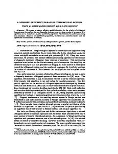
Figure 1: Overall Architecture on MN-MATE
Keywords Manycore, NVRAM, Hybrid Memory, Hierarchical Memory, Memory Management
1.
INTRODUCTION
Emerging manycore computing systems with hundreds or thousands of cores [5] causes severe energy consumption and ever-increasing memory size challenges. The manycore computing system makes it possible to run many applications such as rich multimedia applications and scientific calculations, simultaneously. On the other hand, large amount of memories and storages must be taken into account to execute many processes on the manycore system with high Categories and Subject Descriptors performance and low power. However, the rate of growth B.3.2 [Memory Structures]: Design Styles; D.4.7 [Operating in DRAM memory cannot follow the rate of growth in cores Systems]: Organization and Design [1] and DRAM access latencies cannot be decreased to chase the cpu cycle. This problem is called the ‘memory wall’ [33]. General Terms In this computing environment, increasing the amount of DRAM size and adding more memory channels is not good Design, Management, Performance approach because of the pin limitation of processors. There∗MN-MATE is an abbreviation of Manycore and Nonvolatile fore it cannot increase the bandwidth limitation. This may memory MAnagemenT for Energy efficiency. also lead to severe energy consumed by DRAM. Recent advances such as 3D-stacked memory [13, 17, 16, 18] and nonvolatile memory (NVRAM) [28, 35, 14] have demonstrated orders of magnitude performance and power Permission to make digital or hard copies of all or part of this work for benefits. For instance, 3D-stacked DRAM can significantly personal or classroom use is granted without fee provided that copies are not made or distributed for profit or commercial advantage and that copies increase the memory bandwidth by increasing the width and bear this notice and the full citation on the first page. To copy otherwise, to the frequency of memory bus, and NVRAMs can increase republish, to post on servers or to redistribute to lists, requires prior specific the total amount of a memory with low cost because of its permission and/or a fee. high density and low energy consumption. PMAM 2012, February 26, 2012 New Orleans LA, USA In an attempt to mitigate the energy and memory wall, Copyright 2012 ACM 978-1-4503-1211-0/12/02 ...$10.00.
83
we propose a new architecture with on-chip memory like 3Dstacked DRAM and PRAM which is the one of NVRAMs. In a memory architecture, we propose a hierarchical main memory which consists of on-chip DRAM and a conventional memory placed to off-chip. In addition, we change a conventional off-chip DRAM to a hybrid memory which consists of DRAM and PRAM. Figure 1 shows the proposed overall architecture of MN-MATE. To efficiently operate many applications on the proposed architecture, resource managements must be well implemented for usage of manycores and large amount of various memories. Consequently, we study the software techniques on the proposed hardware architecture. In this paper, we propose three types of techniques to improve the performance and energy consumption, which drive the architecture of our manycore-based system:
Lastly, we propose the simulation platform. Our research ideas aim at the management of manycore and the hierarchical and the hybrid memories. These researches are related to brand-new hardware architectures and special hardware devices such as NVRAMs and on-chip memories. Especially, PRAM is not manufactured in the field. To perform the researches with the proposed MN-MATE platform, we develop the MN-GEMS [9], a timing-aware full system simulator. Our simulation platform addresses the need for manycore support, a timing-aware simulation of multiple types of main memories. Moreover, the simulation platform is open and modular so that it can produce any kind of NVRAMs that we may desire. This study is an extension of our previous work [25], in which we focused on the energy-efficiency with minimal performance loss for the combined architecture of manycore, DRAM, and NVRAM. Our objective in this study, however, is to devise techniques for the hierarchical and hybrid main memory and integrate the overall components in our manycore computing system. The reminder of the paper is organized as follows. Section 2 describes the previous works and section 3 presents the management of proposed memory system. Section 4 presents an example of applications called MaaS. A timingaware full system simulator is presented in Section 5. Our work is concluded in Section 6.
• A hierarchical main memory management: We propose a software-managed memory management by the help of hardware-managed page access monitoring. Because the difference of bandwidth and access latency between a hierarchical memory, we carefully manage an allocation of the pages on on-chip memory to improve the performance. For this purpose, page monitoring module monitors page access patterns during a period, and the OS manages the allocation of pages with collected information. • Power-aware hybrid main memory management [26]: We propose a tchnique for saving total power consumption on a hybrid memory. While the idle power of DRAM is high and increases in proportion to its size, non-volatile memory like PRAM have no idle power. Therefore, using a hybrid memory can be the good approach to decrease consumed power, but PRAM has an endurance problem, long latency to access, and high write energy. It is the reason that the well-organized management scheme is needed. For this purpose, we propose power-aware page migration and culling techniques. • File caching technique based on a hybrid memory [30]: When we use the hybrid memory as a page cache, PRAM memory shows bad write latency and endurance. Thus, the page caching algorithm must consider the different features of memories. We propose a page caching algorithm with prediction and migration. The prediction method is to distinguish page access patterns and the page migration scheme is to maintain write-bound access pages to DRAM. As a case study, we demonstrate the versatility of the MN-MATE platform by showing how MN-MATE can be applied to manycore-based applications. On the top of our platform, we introduce the MaaS (Matching-as-a-Service) [6] application which requires the large amount of memory and high computing power. The MaaS requests high computing power, high memory bandwidth and large amount of memory. The MN-MATE platform can be used because it consists manycore and various memories including a hierarchical and a hybrid memories. In this paper, we introduce the Matching as a Service (MaaS) application. Finally, we show how MN-MATE significantly enhances the system performance in terms of energy consumption and memory access speed.
84
2.
PREVIOUS WORKS
Many researchers have tried to change the current main memory system which uses only DRAM for supporting the large memory requirement of new applications. As the capacity of main memory increases, DRAM main memory shows large power consumption and bandwidth limitation. It also has the scalability wall for sub-45nm technology. In order to solve these drawbacks, on-chip DRAM memory and non-volatile memory technologies are emerging. There are two main memory design options: DRAM-cache and hybrid main memory. DRAM-cache architecture with on-chip memory shows high bandwidth and low latency, and hybrid main memory architecture which combines DRAM with non-volatile memory shows low power consumption. DRAM-cache architecture is introduced for improving the performance gain. L. Zhao et. al. [35] investigate the integration of large capacity, high-bandwidth and low-latency DRAM caches to address memory stall overhead. They also describe the placement of DRAM cache tags and proposed partial on-die tag and sectored cache with prefetching can achieve a performance improvement. However, the tag checking overhead of large caches with small cache line size is nontrivial. To address this issue, Z. Zhang et. al. [34] increase DRAM cache line size. They also propose a prediction technique which accurately predicts the hit/miss status of an access to the cached DRAM, thus reducing the access latency. In the case that uses a large DRAM cache line size, it requires too much bandwidth because the miss rate does not reduce enough to overcome the bandwidth increase. Thus, X. Jiang et. al. [11] propose CHOP (Caching HOt Pages) in DRAM cache to overcome this limitation. By studying several filter-based DRAM caching techniques which are a filter cache, a memory-based filter cache, and an adaptive DRAM caching technique, they achieve a performance improvement and reduce the overhead in tag space. As another method to increase the memory bandwidth, D. H. Woo et.
al. [31] employ a 3D-stacked memory architecture which is placed in the core shows higher bandwidth and lower latency than those of conventional DRAM memory. They propose SMART-3D which is a new 3D-stacked memory architecture with a vertical L2 fetch/write-back network using a large array of through-silicon-vias (TSVs). Moreover, they propose an efficient mechanism to manage the false sharing problem when implementing SMART-3D in a multi-socket system. Therefore, they can take full advantage of this massive bandwidth. For achieving the large main memory capacity, non-volatile memory which has high density and low power consumption characteristics is supposed to be a candidate of main memory. Because non-volatile memory has a limitation in performance, hybrid main memory architecture of DRAM and non-volatile memory is proposed. M. K. Qureshi et. al. [28] and H. Park et. al. [24] use DRAM as a buffer located in front of non-volatile memory which is used for main memory. In order to exploit this architecture efficiently, M. K. Qureshi et. al. present laze-write, line-level writeback, page level bypass, and fine-grained wear-leveling. These techniques can reduce the write count to non-volatile memory and make the write count even among lines of non-volatile memory, thus they can improve performance as well as increase the lifetime of non-volatile memory. H. Park et. al. [24] also introduce runtime-adaptive time out control, DRAM bypassing, and longer time out for dirty data for the power management in the hybrid main memory architecture. These techniques can reduce the energy consumption of main memory with negligible performance overhead. This hybrid main memory architecture shows low power consumption, but additional hardware supports are necessary. In order to reduce additional hardware overhead, G. Dhiman et. al. [8] locates DRAM and non-volatile memory in the same linear region. For exploiting this architecture efficiently, they propose a low overhead hybrid solution for managing memory which consists of the memory allocator and page swapper. The memory allocator serves the memory allocation requests and the page swapper manages the page swap and bad-page interrupts. From these techniques, they can achieve better overall and performance efficiency with negligible overhead. While hybrid main memory architectures which combine DRAM and non-volatile memory can achieve low power consumption and large main memory capacity, they cannot significantly improve performance due to the performance limitation of DRAM and non-volatile memory. In this paper, we propose a hierarchical main memory architecture which combines on-chip memory and a hybrid main memory of DRAM and non-volatile memory. We also present efficient main memory management strategies in this architecture. Finally, we can achieve both high performance and low power consumption with the large capacity of main memory.
3. RESOURCE MANAGEMENT 3.1 Hierarchical Main Memory Management Because on-chip DRAM memory shows higher bandwidth and lower latency than those of conventional DRAM memory, it can be used as a LLC (last level cache) to overcome size limitation of the SRAM caches. Many researches recently have introduced DRAM-cache which uses the on-chip DRAM as a last level cache [17, 11, 31]. DRAM-cache shows
85
Figure 2: Hierarchical main memory architecture and its basic operation
good performance gain when running memory-intensive applications, but L. Zhao et. al. [35] said a scalability problem can occur when the DRAM-cache size increase. Currently, the size of on-chip memory can be increased up to 16GB in the stack [31].
3.1.1
Hierarchical main memory architecture
In this paper, we propose the method to use the on-chip memory as a part of the physically addressable memory. This approach can mitigate the key drawbacks of managing the on-chip memory as a cache, such as tag space overhead and latency of the tag lookup. We propose a hierarchical main memory which consists of two layers, called M1 and M2, shown in Figure 2. M1 memory can be constructed with the on-chip DRAM, and it is placed on a processor. M2 memory is a conventional off-chip DRAM memory. We consider that the hierarchical main memory exclusively arranges through the physical memory area and is physically divided by memory address. On-chip M1 memory which is placed in the core shows higher bandwidth and lower latency than those of M2 onboard DRAM memory. Therefore, many applications want to get many memories of M1 to execute their works faster. Because the size of M1 is limited, many application must contend to obtain large size of M1 memory. For increasing the overall performance and solving the contention problem, software memory management must be needed.
3.1.2
Software memory management
Basic approach is described in Figure 2. During a period, the hardware page access monitor in a memory controller collects information about page accesses. At the end of the period, the OS uses the collected information to decide a new memory mapping. The key assumption of this approach is that the page access pattern in one period is similar to the next pattern in the next period. The OS will migrate the most frequently accessed pages into M1 memory and move the less accessed pages in M1 memory to M2 memory. The LLC misses are handled by the memory controller and cause the memory requests. The memory controller can watch the all memory requests so that it can monitor the page access pattern. We add a page access monitor module in the memory controller and this monitor gathers a list
of the most frequently accessed pages. To monitor the page accesses, a monitor module maintain page access maps which consist of page address and counter, as shown in Figure 2. Whenever a memory request occurs, it finds the matched page access map with a page address and a corresponding counter value is increased by one. If there is no matched one, new page access map is created and added to a list. We construct two lists to store the history of page accesses. Actually, the memory controller cannot log all kinds of pages during the operation. Therefore, we should design the monitoring method with small size of page access maps. It the first level, we designed it contains the most frequently accessed pages. It is managed with LFU-like replacement policy. If one page access map is removed from the first level by adding new one, the count value of this page will be lost and the corresponding page also lose the chance to move to the first level with a next access. To store the history of the pages, we add the second level of the list and the second level is managed by LRU replacement policy, as shown in Figure 2. If a hit on the second level occurs and the counter value is equal to the minimum of the first level, this page access map moves to the first level to the next page access map with greater than the value. At every period, the OS obtains the information of page access pattern from monitoring module , determine allocations of pages, and then migrates the most frequently accessed pages to the M1 memory. In our proposed scheme, the pages in the first level list are the most frequently accessed pages during one period so that the OS will allocate all pages in the first level into the M1 memory.
(a) Hit ratio on m1 memory
(b) IPC Figure 3: Hit ratio on M1 memory and IPC with 32MB size of M1 memory
3.1.3 Preliminary evaluation In order to evaluate the proposed memory management scheme for the hierarchical main memory, we made a simulator based on Pin [19]. In this section, we present the performance results of our proposed scheme for the hierarchical main memory. As workloads for evaluation, we selected the SPEC CPU2006 benchmark [3]. The preliminary experiments are conducted with a single application. We evaluated our management scheme and compare the hit ratio on the M1 memory and IPC (instruction per cycle). From Figure 3(a), we can know that the hit ratio is highest when we utilize the M1 memory as DRAM cache. However, if we watch the IPC, our scheme shows the better performance, as shown in Figure 3(b). It is because that if we use DRAM cache, DRAM should be accessed twice for looking up tags and for reading data.
3.2 Power-aware Hybrid Main Memory Management
Figure 4: Hybrid Main Memory Architecture
For the MN-MATE system, we consolidate both DRAM and PRAM into hybrid main memory to save the energy. The idle power of DRAM has non-negligible effect on the total power consumption, and it has increased in proportion to its size [22]. On the contrary, non-volatile memories such as PRAM have no refresh power and low idle power. These emerging memories can be good candidates for replacing DRAM in terms of energy. However, PRAM has some vulnerabilities such as limited write endurance about 108 , long latency to access, and high write energy compared to DRAM [14].
Figure 4 shows the simplified hybrid main memory architecture. The hybrid main memory consists of DRAM and PRAM. This heterogeneous memory chips are wired with same memory controller, then they are assigned to linear physical addresses and both regions can be accessed by memory controller directly. This architecture has several advantages compared to another approach [28] which is composed of DRAM cache and PRAM main memory. Though cache architecture provides a decrease in write count of PRAM, it has a overhead to access data in PRAM due to copy operation from PRAM
3.2.1 Hybrid main memory architecture
86
Figure 5: Power-aware Page Migration and Culling (a) Energy Saving
to DRAM when cache miss occurs. And DRAM which is only used for cache cannot increase the total size of main memory. However, linear architecture described in Figure 4 is possible to aggravate both performance and energy consumption if many memory operations occur in PRAM [8]. Therefore, it should be well-managed to alleviate disadvantages of PRAM.
3.2.2 Management scheme We propose memory management mechanism to take advantages of hybrid memory architecture. The management unit is a page because the page is the basic unit of management in OS. Figure 5 describe the schemes to manage the memory system. First scheme is hot/cold separation in page level. Because PRAM has long latency, high write energy and limited endurance, hot pages should be in DRAM and cold pages in PRAM is more beneficial. We have used access bit in the page table entry to separate hot pages. We use second chance algorithm to identify the characteristics of pages, then two consecutive memory references mean a hot page and two consecutive non-references mean a cold page. Second, we migrate the hot pages to DRAM and cold pages to PRAM. Using this manner, we can obtain both improvement of performance and power. Migrate operation is accomplished by the OS periodically. Moreover, we can reduce main memory’s power consumption by turning off unused DRAM region. This turning off function is supported in some mobile DRAM. In order to turn off the region of DRAM, active region should be swept. Therefore we propose page culling and gathering which sweep DRAM region which contains few used pages and compulsorily migrate those pages to PRAM as shown in Figure 5. It always searches for free pages in online DRAM region and helps minimize DRAM idle power.
(b) Performance Overhead Figure 6: Energy Saving and Performance Overhead Results
is used as a page cache to hide disk access latency. Many page caching algorithms such as LRU [7], LIRS [10], and CLOCK-Pro [27] have been developed for current DRAM based main memory. In addition, FBR [29], LRU-2 [23], 2Q [12], LRFU [15], and MQ [36] were proposed and researchers tried to combine ”recency” (LRU) and ”frequency” (LFU) in order to compensate for the disadvantages of LRU. However, such previous page caching algorithms only considered the main memory with uniform access latency and unlimited endurance. They cannot be directly adapted to the hybrid main memory architecture with DRAM and PRAM. The main objective of this work is to propose a new page caching algorithm for the hybrid main memory. The algorithm is designed to overcome the long latency and endurance problem of PRAM. On the basis of conventional cache replacement algorithms, we propose a prediction of the page access pattern by page monitoring and migration schemes to move write-bound access pages to DRAM.
3.2.3 Energy saving We implement all these schemes in Linux operating system. For migration, we used virtual NUMA nodes to divide DRAM and PRAM region. Migration operation is done by kernel daemon we implemented. For evaluation, we use cycle accurate simulator to count memory accesses. The experimental results show that the proposed techniques can reduce the energy consumption by up to 35% with 5% delay overhead of memory access.
3.3.1
Prediction and page migration scheme
To satisfy the requirements, we add a prediction of page access pattern and migration schemes. In order to monitor the pages and to adapt the migration scheme, we use four monitoring queues, which consist of a DRAM read queue, a DRAM write queue, a PRAM read queue, and a PRAM write queue, as shown in Figure 7. When one page block is accessed, it is retained into both the LRU list and one of
3.3 File Caching Technique based on the Hybrid Memory In modern computer systems, a large part of main memory
87
the four queues by its access pattern and the memory type where it is located. To solve performance degradation and worn-out problem caused by PRAM’s long latency and low endurance, we use migration of pages between DRAM and PRAM. We move the write-bound pages from PRAM to DRAM. Additionally, we move the read-bound pages from DRAM to PRAM. Before deciding the page migration, we have to know which pages are write-bound and which pages are read-bound. For prediction of the access pattern, we calculate the weighting values, which indicate how close the values are to writebound or read-bound. By monitoring the request types of the page requests, the weighting value can be calculated by using a moving average with weight α ∈ [0, 1] as follows: Wcur = αWprev + (1 − α)RT
(1)
, where RT means the requested type of the page; its value is 1 if the page request is write and −1 if the page request is read. There are two migration cases: one is the migration of write-bound pages from PRAM to DRAM; the other is the migration of read-bound pages from DRAM to PRAM. According to equation 1, the Wcur is increased when write requests occur and is decreased at every read request. Algorithm 1 shows how the cached pages are migrated. For example, if the write access is hit on a page in the PRAM write queue, PW, as shown in Figure 7, and its weighting value is over T rmig , this page will migrate to the DRAM write queue. We use two threshold values for determining the migration and the movement between read and write queues in the same memory. T rmig is the threshold value for determining whether a page is migrated and T rq is the threshold value for determining movement between read and write queues. Two threshold values are determined through experiments.
Figure 7: Monitoring queues and an example of migration of the write-bound pages
from PRAM to DRAM. If there is no free space in DRAM, we select a victim page from the bottom of the DRAM read queue and remove it from DRAM. The write-bound page in PRAM is moved to the DRAM where the victim page was located. In the DRAM write queue, this page is put into the top of the queue. In case of the victim page, we just drop the page because it may increase PRAM write count if we move the victim page to PRAM. If there is no element in the DRAM read queue when we find a victim page for migration, we choose a victim page from the bottom of the DRAM write queue, which means that the victim page is the least recently used. The migration of read-bound pages is similar to the migration of write-bound pages.
Algorithm 1 : Page Migration Function input: page address and request type Wcur : Current weight value T rmig : Threshold value for determining migration T rq : Threshold value for determining movement between read and write queues
3.3.2
Experiment results of hit ratio and write count
The hybrid main memory is defined in Figure 4. Because PRAM density is expected to be four times higher than that of DRAM [25, 32], we mainly allocate four times larger amount of memory to PRAM in this experiment. To evaluate the performance characteristics of the proposed page caching algorithm, we constructed a trace-driven simulator and used the OLTP traces. These traces were made available courtesy of Ken Bates from HP, Bruce McNutt from IBM, and the Storage Performance Council [2]. We selected the parameter, α, in the equation 1 and two threshold values in Algorithm 1 through experiments. We select the values of α, T rmig and T rq as 0.5, 0.5 and 0.35, respectively. The first experiment measures the hit ratio, which is important in determining the performance of the page caching algorithm. We compared the hit ratio of our page caching algorithm to the hit ratios of the conventional page caching algorithms. The results are shown in Figure 8(a). From the results, while the hit ratio of our algorithm is lower than that of LRU, the results show that the hit ratio is similar to those of the LRU, LIRS, and CLOCK-Pro algorithms. Because we designed the selected victim page for migration to simply be eliminated, it is possible that the page faults will occur more. The second experiment shows the total write access count on PRAM, which is also important because it
Calculate Wcur if page in PRAM then if Wcur ≥ T rmig then migrate the page to DRAM else if Wcur ≥ T rq and page in read queue then the page moves to write queue else if Wcur ≤ −T rq and page in write queue then the page moves to read queue end if else if page in DRAM then if Wcur ≤ −T rmig then migrate the page to PRAM else if Wcur ≤ −T rq and page in write queue then the page moves to read queue else if Wcur ≥ T rq and page in read queue then the page moves to read queue end if end if Figure 7 shows an example of write-bound page migration
88
(a) Hit ratio
Figure 9: Example Service of MaaS
(b) The total write access count on PRAM Figure 8: Experiment results of the proposed and conventional algorithms on financial1 workload
is related to the total latency of the page cache and the lifetime of PRAM. Figure 8(b) shows the total number of write accesses on PRAM with financial1 workloads. When using our algorithm, we can know that the total number of write accesses is reduced compared to that for the conventional page caching algorithm. We can reduce the total write access count by a maximum of 52.9%.
Figure 10: Memory Characterization of MaaS System
ternet broadcast vendors, and movie film makers want to use multimedia analyzing service for automatic-advertising, deduplication of multimedia contents, or multimedia web searching, they will request above kinds of service to image analysis service providers. MaaS system’s computation power, resource, and several image analyzing algorithm are rent to the service providers. If service providers transmit contents providers’ input stream to MaaS, then MaaS send mathcing results which are followed service provider’s conditions. For example, if service providers want to receive images which are similar to their input, MaaS will give matched images finding from DB. To realize this system, accelerating image analysis power and well-managed resource are important. MaaS operation consists of the feature extraction and the feature matching operation. It requires the large main memory capacity and power consumption. Therefore, the MNMATE platform is a suitable candidate because it has the hierarchical and hybrid main memory architecture which has the large memory capacity and low power consumption characteristics. MaaS operation shows the complex computational overhead. The MN-MATE platform can solve this limitation with manycore CPUs and general purpose GPUs. First, the feature extraction in MaaS operation has parallel operations, thus it can be accelerated by manycore CPUs and general purpose GPUs which are optimized for the parallel processing. Second, the matching operation matched the uploaded images and videos with data in the image
4. CASE STUDY: MATCHING AS A SERVICE (MAAS) With the advancement of digitalization and the availability of communication networks, multimedia matching services such as Picasa, Pudding application, and Google Goggles have become increasingly popular services. To realize the services, many vendors constructed their systems based on their own ways which prevents people from taking advantage of a high-quality multimedia matching services. However, they have been unable to share a well-defined multimedia matching library and united multimedia database. To alleviate this limitation, we suggest an open and highquality matching service, called ”Multimedia Matching as a Service (MaaS)”. MaaS can analyze the multimedia input stream and search the image which has similar features with the input data at the multimedia database. It can also accelerate the image analysis procedure by exploiting the resources of MN-MATE platform which are manycore CPUs, general-purpose GPUs, and hierarchical and hybrid main memory. Thus, users can take the high quality multimedia matching services, shared multimedia databases, and a well-defined multimedia matching library. Figure 9 shows an example of MaaS’s service flow. When contents providers such as SmartTV Broadcast vendors, In-
89
database. The file caching technique based on the hybrid memory can reduce the performance overhead by I/O operations in the matching operation. By caching hot data in DRAM and cold data in PRAM, we can improve performance of the matching operation. During the feature extraction and the feature matching operation, the main memory is largely used for storing uploaded images and videos and data from the image database. Therefore, we can exploit the management scheme in the hierarchical main memory system and the hybrid main memory system in order to use the main memory efficiently. Figure 10 shows the memory access of MaaS which can be divided into hot and cold region. In both main memory systems, they use hot/cold separation scheme that locates hot memory access into M1 memory/DRAM and cold memory into M2 memory/PRAM. We can improve performance of MaaS by exploiting resource management of MN-MATE platform.
5. MN-GEMS: A TIMING-AWARE FULL SYSTEM SIMULATOR
Figure 11: An example of modeled hardware and execution environment in the simulator.
Our research ideas, including results from the first year MN-MATE [25], aimed at the management of manycore and various memory hierarchies including on-chip memory and NVRAMS, which are not manufactured in the field, yet. As a fundamental way of performing this kind of research, simulation-based designs and evaluations stand out as the most widely used mechanisms. The use of software simulators allows the validation of architecture designs and the exploration of new concepts before actual implementation. Thus, there is a need for a well-defined simulation environment for the study on the manycore system and the various memory hierarchy-based system design. By thoroughly investigating our research direction, we identified three requirements for the simulation environment construction: 1) support for manycore simulation; 2) timing-aware simulation of hybrid main memory hierarchy based on the on/offchip DRAM and NVRAM access characteristics; and 3) a Performance Monitoring Unit (PMU).
To alleviate these limitations, we realized a more advanced simulation platform, MN-GEMS, which meets the above requirements. GEMS is considered a promising foundation for our simulation platform. Our simulation platform addresses the need for manycore support, a timing-aware simulation of multiple types of main memory, and a PMU by devising a memory traffic multiplexer and a reconfigurable memory controller. Moreover, the simulation platform is open and modular, allowing simulation users to produce any kind of DRAM and NVRAM that they may desire. Our MN-GEMS simulation platform will be used as one of the base simulator for ongoing research issues in the MN-MATE project.
5.1
Table 1: Functionalities of full-system simulators Manycore M5 [4] Simics [20] GEMS [21] MN-GEMS
X O O O
Timing Simulation DRAM NVRAM O X X X O X O O
PMU
Acceleration
X X X O
X X X O
Details of Simulation Platform
The primary purpose of MN-GEMS is to simulate a MNMATE node equipped with manycore and a hierarchical and a hybrid main memory. To meet this requirement, the simulator models a hardware shown in Figure 11 and performs a full-system simulation. We built the MN-GEMS by configuring GEMS to support manycore and adding modified cache hierarchy, on/off-chip DRAM hierarchy modules, a NVRAM timing simulation module and a PMU.
5.1.1
Manycore support
To simulate manycore processors, we configured GEMS so that a processor consists of 8 cores, core-private L1 caches, and a shared L2 last level cache (LLC). All cores in the processor share same LLC. Access to the caches for any task is delayed in accordance with the memory timing model.
Table 1 shows the functionalities of conventional simulation platforms. The last row in Table 1 clarifies our simulation design goal with respect to desirable functionalities to be achieved. Among the five requirements, M5 and Simics provide only one functionality, even though they support a full-system simulation. They give little consideration to the different access latencies that are in accord with the NVRAM access type and to the memory access request ordering generated from manycore. Even though GEMS has attained a consensus that it can enable DRAM timing simulation functionality as well as manycore support, it cannot support an on/off-chip DRAM and an NVRAM timing simulation, runtime feedback of performance statistics. Finally, previous simulators have not offered much of a solution to reducing long simulation times when timing-awareness feature is enabled with a full-system simulation.
5.1.2
Timing-aware simulation
The goal of a timing-based simulation is to get results of both the execution result and the latency generated by event handling. GEMS basically provides timing-based simulation modules with the timing parameters from on-chip DRAM [31] and off-chip DDR2 SDRAM. We built another timing-based simulation module for the timing parameters of NVRAM and added a request controller to both of memories. The overall procedure for the timing-aware memory access timing simulation is shown in Figure 12. If a task accesses memory, a memory access request is generated and issued to the request controller. The issued request is inserted into
90
7.
ACKNOWLEDGMENTS
The work presented in this paper was supported by MKE (Ministry of Knowledge Economy, Republic of Korea), Project No. 10035231-2010-01.
8.
Figure 12: Internal procedure of timing-aware simulation one of two controllers according to the target memory type of the request. In the request controller, requests are sorted so that requests with the highest priority are issued first. If issued, the state of the issued request is changed to issued and waits for the specified time. When the request is done, a response is sent back to the requester.
5.1.3 Performance monitoring of tasks The memory access pattern of a task is one of the most useful hints to predict future memory contention when scheduled simultaneously with other tasks. We added a PMU to the hybrid main memory and the caches in the processor to monitor per-task access patterns. With a number of counter registers, it monitors the occurrence of concerned events such as LLC misses, cache line fills, DRAM reads/writes, and NVRAM reads/writes. When an administrative task in the hypervisor, guest OS, or any application needs to get values from the PMU, it executes a magic instruction. The magic instruction pauses the current simulation and copies values from the PMU to the predetermined memory location. Then, the simulation resumes and the caller can access the collected data.
5.2 Current Status and Next Steps We are still in the phase of accelerating simulation speed to prove our idea regarding resource management for the MN-MATE project. Once the simulator is ready to execute fast enough, we plan to investigate performance bottlenecks to exhibit our motivation and to prove the efficiency of our solution regarding resource management.
6. CONCLUSIONS In this paper, we presented MN-MATE platform including a hierarchical and a hybrid main memories and management techniques for highly utilizing the proposed architecture. As memory management techniques, we presented the hierarchical main memory management and the poweraware hybrid main memory management, which shows good performance and energy-efficiency. In addition, we deal with the file caching on the hybrid memory. We presented the proper caching algorithm based on the hybrid memory. Although some hardware devices on the MN-MATE platform are not manufactured in the field, we designed the full system simulator, MN-GEMS, for the study on the manycore system and its management technique. We are currently implementing MN-MATE hardware and software components including memory managements and MaaS application. We will soon have complete design and implementation about managements of the proposed memory architecture and the MaaS service.
91
REFERENCES
[1] Hp. memory technology evolution: an overview of system memory technologies., http://tinyurl.com/ctfjs2. [2] Oltp application i/o and search engine i/o. umass tracerepository, http://traces.cs.umass.edu/index.php/storage/storage. [3] Spec’s benchmark, http://www.spec.org/cpu2006. [4] N. Binkert, R. Dreslinski, L. Hsu, K. Lim, A. Saidi, and S. Reinhardt. The m5 simulator: Modeling networked systems. Micro, IEEE, 26(4):52 –60, july-aug. 2006. [5] S. Borkar. Thousand core chips: a technology perspective. In Proceedings of the 44th annual Design Automation Conference, DAC ’07, pages 746–749, New York, NY, USA, 2007. ACM. [6] J. H. Choi, K.-W. Park, S. K. Park, and K. H. Park. Multimedia matching as a service: Technical challenges and blueprints. In The 26th International Technical Conference on Circuits/Systems, Computers and Communications, 2011. [7] A. Dan and D. Towsley. An approximate analysis of the lru and fifo buffer replacement schemes. Proceedings of the 1990 ACM SIGMETRICS conference on Measurement and modeling of computer systems, pages 143–152, April 1990. [8] G. Dhiman, R. Ayoub, and T. Rosing. Pdram: A hybrid pram and dram main memory system. In Design Automation Conference, 2009. DAC ’09. 46th ACM/IEEE, pages 664 –669, july 2009. [9] W. Hwang, K.-W. Park, and K. H. Park. Mn-gems: A timing-aware simulator for a cloud node with manycore, dram, and non-volatile memories. In Cloud Computing (CLOUD), 2011 IEEE International Conference on, pages 734 –735, july 2011. [10] S. Jiang and X. Zhang. Lirs: An efficient low inter-reference recency set replacement policy to improve buffer cache performance. In Marina Del Rey, pages 31–42. ACM Press, 2002. [11] X. Jiang, N. Madan, L. Zhao, M. Upton, R. Iyer, S. Makineni, D. Newell, Y. Solihin, and R. Balasubramonian. Chop: Adaptive filter-based dram caching for cmp server platforms. In High Performance Computer Architecture (HPCA), 2010 IEEE 16th International Symposium on, pages 1 –12, jan. 2010. [12] T. Johnson and D. Shasha. 2q: A low overhead high performance buffer management replacement algorithm. In Proceedings of the 20th International Conference on Very Large Data Bases, VLDB ’94, pages 439–450, San Francisco, CA, USA, 1994. Morgan Kaufmann Publishers Inc. [13] T. Kgil, S. D’Souza, A. Saidi, N. Binkert, R. Dreslinski, T. Mudge, S. Reinhardt, and K. Flautner. Picoserver: using 3d stacking technology to enable a compact energy efficient chip multiprocessor. In Proceedings of the 12th
[14]
[15]
[16]
[17]
[18]
[19]
[20]
[21]
[22]
[23]
[24]
international conference on Architectural support for programming languages and operating systems, ASPLOS-XII, pages 117–128, New York, NY, USA, 2006. ACM. B. C. Lee, E. Ipek, O. Mutlu, and D. Burger. Architecting phase change memory as a scalable dram alternative. In Proceedings of the 36th annual international symposium on Computer architecture, ISCA ’09, pages 2–13, New York, NY, USA, 2009. ACM. D. Lee, J. Choi, J.-H. Kim, S. H. Noh, S. L. Min, Y. Cho, and C. S. Kim. Lrfu: A spectrum of policies that subsumes the least recently used and least frequently used policies. IEEE Transactions on Computers, 50(12):1352–1361, December 2001. C. Liu, I. Ganusov, M. Burtscher, and S. Tiwari. Bridging the processor-memory performance gap with 3d ic technology. Design Test of Computers, IEEE, 22(6):556 – 564, nov.-dec. 2005. G. H. Loh. 3d-stacked memory architectures for multi-core processors. In Proceedings of the 35th Annual International Symposium on Computer Architecture, ISCA ’08, pages 453–464, Washington, DC, USA, 2008. IEEE Computer Society. G. L. Loi, B. Agrawal, N. Srivastava, S.-C. Lin, T. Sherwood, and K. Banerjee. A thermally-aware performance analysis of vertically integrated (3-d) processor-memory hierarchy. In Proceedings of the 43rd annual Design Automation Conference, DAC ’06, pages 991–996, New York, NY, USA, 2006. ACM. C.-K. Luk, R. Cohn, R. Muth, H. Patil, A. Klauser, G. Lowney, S. Wallace, V. J. Reddi, and K. Hazelwood. Pin: building customized program analysis tools with dynamic instrumentation. In Proceedings of the 2005 ACM SIGPLAN conference on Programming language design and implementation, PLDI ’05, pages 190–200, New York, NY, USA, 2005. ACM. P. Magnusson, M. Christensson, J. Eskilson, D. Forsgren, G. Hallberg, J. Hogberg, F. Larsson, A. Moestedt, and B. Werner. Simics: A full system simulation platform. Computer, 35(2):50 –58, feb 2002. M. M. K. Martin, D. J. Sorin, B. M. Beckmann, M. R. Marty, M. Xu, A. R. Alameldeen, K. E. Moore, M. D. Hill, and D. A. Wood. Multifacet’s general execution-driven multiprocessor simulator (gems) toolset. SIGARCH Comput. Archit. News, 33:92–99, November 2005. D. Meisner, B. T. Gold, and T. F. Wenisch. Powernap: eliminating server idle power. In Proceedings of the 14th international conference on Architectural support for programming languages and operating systems, ASPLOS ’09, pages 205–216, New York, NY, USA, 2009. ACM. E. J. O’Neil, P. E. O’Neil, and G. Weikum. The lru-k page replacement algorithm for database disk buffering. In Proceedings of the 1993 ACM SIGMOD international conference on Management of data, SIGMOD ’93, pages 297–306, New York, NY, USA, 1993. ACM. H. Park, S. Yoo, and S. Lee. Power management of hybrid dram/pram-based main memory. In Design
[25]
[26]
[27]
[28]
[29]
[30]
[31]
[32]
[33]
[34]
[35]
[36]
92
Automation Conference (DAC), 2011 48th ACM/EDAC/IEEE, pages 59 –64, june 2011. K. H. Park, Y. Park, W. Hwang, and K.-W. Park. Mn-mate: Resource management of manycores with dram and nonvolatile memories. In High Performance Computing and Communications (HPCC), 2010 12th IEEE International Conference on, pages 24 –34, sept. 2010. Y. Park, D.-J. Shin, S. K. Park, and K. H. Park. Power-aware memory management for hybrid main memory. In Next Generation Information Technology (ICNIT), 2011 The 2nd International Conference on, pages 82 –85, june 2011. S. J. Performance and S. Jiang. Clock-pro: An effective improvement of the clock replacement. In Proceedings of USENIX Annual Technical Conference, 2005. M. K. Qureshi, V. Srinivasan, and J. A. Rivers. Scalable high performance main memory system using phase-change memory technology. In Proceedings of the 36th annual international symposium on Computer architecture, ISCA ’09, pages 24–33, New York, NY, USA, 2009. ACM. J. T. Robinson and M. V. Devarakonda. Data cache management using frequency-based replacement. In Proceedings of the 1990 ACM SIGMETRICS conference on Measurement and modeling of computer systems, SIGMETRICS ’90, pages 134–142, New York, NY, USA, 1990. ACM. H. Seok, Y. Park, K.-W. Park, and K. H. Park. Efficient page caching algorithm with prediction and migration for a hybrid main memory. SIGAPP Appl. Comput. Rev., 11(4):38–48, Dec. 2011. D. H. Woo, N. H. Seong, D. Lewis, and H.-H. Lee. An optimized 3d-stacked memory architecture by exploiting excessive, high-density tsv bandwidth. In High Performance Computer Architecture (HPCA), 2010 IEEE 16th International Symposium on, pages 1 –12, jan. 2010. X. Wu, J. Li, L. Zhang, E. Speight, R. Rajamony, and Y. Xie. Hybrid cache architecture with disparate memory technologies. In Proceedings of the 36th annual international symposium on Computer architecture, ISCA ’09, pages 34–45, New York, NY, USA, 2009. ACM. W. A. Wulf and S. A. McKee. Hitting the memory wall: implications of the obvious. SIGARCH Comput. Archit. News, 23:20–24, March 1995. Z. Zhang, Z. Zhu, and X. Zhang. Design and optimization of large size and low overhead off-chip caches. Computers, IEEE Transactions on, 53(7):843 – 855, july 2004. L. Zhao, R. Iyer, R. Illikkal, and D. Newell. Exploring dram cache architectures for cmp server platforms. In Computer Design, 2007. ICCD 2007. 25th International Conference on, pages 55 –62, oct. 2007. Y. Zhou, J. Philbin, and K. Li. The multi-queue replacement algorithm for second level buffer caches. In Proceedings of the General Track: 2002 USENIX Annual Technical Conference, pages 91–104, Berkeley, CA, USA, 2001. USENIX Association.


![Construction of a Hierarchical]Â¥ anslation Memory](https://m.moam.info/img/260x300/construction-of-a-hierarchicala-anslation-memory_5bac5a4e097c47c72a8b4597.jpg)


