the main radiation characteristics of parallel-plate slot antennas. The results using these structures in comparison with conventional perfect electric conductor ...
modulation, propagated through a CFBG acting as optical phase controller of a mm-wave downstream fiber link, has been demonstrated. Up to 2.5 Gb/s on a 40-GHz carrier have been transmitted with no dispersion power penalty and BER ⬍10⫺9. REFERENCES
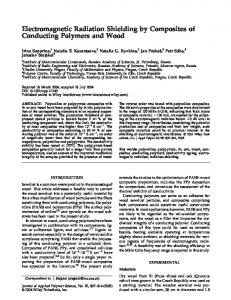
Figure 8 Bit-error-rate measurements as function of the received optical power for 1- and 2.5-Gb/s data transmission with and without the CFBG with dispersion of 280 ps/nm. Eye patterns for a BER of 10⫺9 when the CFBG is used are shown in the insets
7 shows the photonic-link setup. The mm-wave carrier is created by a dual-frequency optical source based on a DSB-CS modulation of a laser. The optical sidebands generated in the modulation are divided into two separated fibers by filtering with FBGs of narrow bandwidth. One of the waves is modulated with baseband data. The signals are combined and connected to the base station through a CFBG, which is the dispersive element whose performance for propagating data with this type of link is tested. At the base station, the mm-wave modulated with data is created with a wide bandwidth photodetector through heterodyne mixing of the two optical waves. This mm-wave is amplified and transmitted to the mobile unit, where the reception is performed using selfhomodyne mixing [12]. At the present experiment, in order to avoid free-space mm-wave transmission effects, so that the optical effects would be isolated so as to be properly studied, a cable with no amplification was used as the transmission link between the base station and the mobile unit instead of antennas. Data transmission was carried out at 1 and 2.5 Gb/s on a 40-GHz mm-wave generated with this DSB-CS modulation-based link. The bit-error rate (BER) was measured versus the received optical power at the photodiode. The BER measurements are shown in Figure 8 for 1- and 2.5-Gb/s data transmission with and without CFBG acting as phase controller. The word length was 27 ⫺ 1. No power penalty due to the chromatic dispersion induced by the gratings was observed due to the DSB-CS modulation. The low sensitivity of the system (⫺3 dBm for 1 Gb/s) was due to limited mm-wave amplification in the reception. CONCLUSION
The two 1st harmonics of the mm-wave output signal of a photonic downstream transmission fiber link have been measured. The effects on the carried power by these two harmonics due to the high-order modulation optical sidebands have been analysed. In the case of DSB conventional modulation it is found that the second harmonic is degradated due to the sidebands of order ⫾2. When DSB-CS modulation is utilized, it is shown that the residual optical carrier does not produce a 1st harmonic with significant power level. Furthermore, the combination of the residual optical carrier with the optical sidebands does not degradate the power level of the 2nd harmonic. Hence, it can be used for data transmission. Data transmission utilizing DSB-CS
DOI 10.1002/mop
1. G.J. Meslener, Chromatic dispersion induced distortion of modulated monochromatic light employing direct detection, IEEE J Quant Electron 20 (1984), 1208 –1218. 2. J. Marti, F. Ramos, and J. Herrera, Experimental reduction of dispersion-induced effects in microwave optical links employing SOA boosters, IEEE Photon Technol Lett 13 (2001), 999 –1001. 3. P. Laurencio and M.C.R. Madeiros, Dynamic range of optical links employing optical single side-band modulation, IEEE Photon Technol Lett 15 (2003), 748 –750. 4. D.H. Smith, D. Novak, and Z. Ahmed, Novel technique for generation of optical SSB with carrier using a single MZM to overcome fiber chromatic dispersion, Int Topical Mtg Microwave Photon, Kyoto, Japan, 1996, paper PDP-2. 5. D.S. Glassner, M.Y. Frankel, and R.D. Esman, Reduced loss microwave fiber-optic links by intracavity modulation and carrier suppression, IEEE Microwave Guided Wave Lett 7 (1997), 57–59. 6. Y. Miyamoto, A. Hiramo, S. Kuwahara, M. Tomizawa, and Y. Tada, Novel modulation and detection for bandwidth-reduced RZ formats using duobinary-mode splitting in wideband PSK/ASK conversion, J Lightwave Technol 20 (2002), 2067–2077. 7. J. Yu and G.-K. Chang, A novel technique for optical label and payload generation and multiplexing using optical carrier suppression and separation, IEEE Photon Technol Lett 15 (2004), 320 –321. 8. S. Shimotshu, O. Oikawa, T. Saitou, N. Mitsugi, K. Kuboreda, T. Kawanishi, and M. Izutsu, Single-sideband modulation performance of LiNbO3 integrated modulator consisting of four-phase modulator waveguides, IEEE Photon Technol Lett 13 (2001), 364 –366. 9. P. Pe´rez-Milla´n, S. Torres-Peiro´, J. Mora, A. Dı´ez, J.L. Cruz, and M.V. Andre´s, Electronic tuning of delay lines based on chirped fiber gratings for phased arrays powered by a single optical carrier, Optics Commun 238 (2004), 277–280. 10. K.-M. Feng, J.-X. Cai, V. Grubsky, D.S. Starodubov, M.I. Hayee, S. Lee, X. Jiang, A.E. Willner, and J. Feinberg, Dynamic dispersion compensation in a 10-Gb/s optical system using a novel voltage tuned nonlinearly chirped fiber Bragg grating, IEEE Photon Technol Lett 11 (1999), 373–375. 11. J.L. Corral, J. Martı´, J.M. Fuster, and R.I. Laming, Dispersion-induced bandwidth limitation of variable true time delay lines based on linearly chirped fibre gratings, Electron Lett 23 (1998), 209 –211. 12. A. Wiberg, P. Pe´rez-Milla´n, M.V. Andre´s, P.A. Andrekson, and P.O. Hedekvist, Fiber optic 40-GHz mm-wave link with 2.5-Gb/s data transmission, IEEE Photon Technol Lett 17 (2005), 1938 –1940. © 2006 Wiley Periodicals, Inc.
ELECTROMAGNETIC BANDGAP STRUCTURES AS ARTIFICIAL MAGNETIC CONDUCTOR SURFACES SIDEWALLS IN PARALLEL PLATE SLOT ANTENNAS J. M. Ferna´ndez and M. Sierra-Castan˜er Radiation Group Department of Signals, Systems and Radio-Communications Polytechnic University of Madrid 28040 Madrid, Spain Received 13 January 2006 ABSTRACT: Metamaterial structures have unique properties in controlling the propagation of electromagnetic waves. In this work we ana-
MICROWAVE AND OPTICAL TECHNOLOGY LETTERS / Vol. 48, No. 7, July 2006
1441
lyze the effect of a metamaterial denominated EBG structures acting as if they had artificial magnetic conductor (AMC) properties to enhance the main radiation characteristics of parallel-plate slot antennas. The results using these structures in comparison with conventional perfect electric conductor (PEC) sidewalls in a planar slot antenna are presented as an example of application. © 2006 Wiley Periodicals, Inc. Microwave Opt Technol Lett 48: 1441–1446, 2006; Published online in Wiley InterScience (www.interscience.wiley.com). DOI 10.1002/mop. 21633 Key words: artificial magnetic conductors; electromagnetic bandgap structures; high-impedance surfaces; metamaterials; parallel-plate waveguides; planar slot antennas 1. INTRODUCTION
Metamaterials are novel artificial periodic structures that have been investigated for their versatility in controlling the propagation of electromagnetic waves in one, two, or three dimensions. These structures are artificially engineered material structures that exhibit novel properties in comparison with the constituent homogeneous materials used to manufacture them. That allows designing new materials with properties that are not available in conventional materials. Recent studies on metamaterial structures have revealed that they are numerous applications able to enhance the performance of antennas and microwave circuits [1]. Because of their different classes, they can satisfy such as artificial magnetic conductor (AMC) properties or high-impedance surfaces (HIS), frequency-selective surface (FSS) structures, electromagnetic/photonic bandgap (EBG/PBG) materials, and creation of materials with negative permittivity and negative permeability called lefthanded medium (LHM). To date, AMC surfaces are receiving more and more attention because of their interesting properties that may overcome some of the problems of traditional perfect electric conductor (PEC) surfaces. In contrast with the realization of the PEC condition, the realization of AMC conditions remains as a difficult task because of the nonexistence of materials with these properties in nature. Two basis classes of artificial magnetic surfaces have emerged: those based on a volume of artificial material and those based on a surface distribution of inhomogeneities. The mushroom structure of Sievenpiper et al. is a member of the first class [2]. For the second class surfaces composed of 2D square lattice with Jerusalem crosses as proposed by Itoh et al. is a good example [3]. These two surfaces belong to the class of electromagnetic bandgap structures that exhibit rich physical effects. In that way, one possibility to model AMC behaviour is to use EBG periodic structures as analyzed by Itoh in [4], which are extremely easy to design and fabricate, in contrast to many of other surfaces described in previous published work [5]. AMC are not a new concept, of course. Corrugated planes and cylinders found early use as waveguides for surface wave and end-fire antennas (see, for example, [6, 7]). The majority of previously published works have proposed and analyzed several examples designs of AMC and HIS surfaces with 3D or 2D inhomogeneous structure or with lumped elements [8]. But we did not found a lot of practical antennas applications with these AMC properties. Later on, Itoh et al. analyzed a standard rectangular waveguide with EBG structures acting as perfect magnetic conductor (PMC) sidewalls to find applications in designing novel TEM standard rectangular waveguides [9]. Recent works by Feresidis et al. used AMC surfaces as an AMC ground plane to suppress the unusual reflection phase for gain enhancement of low-profile high-gain antennas [10]. This work differs from previously published contributions because, in this case, AMC surfaces have been applied and analyzed
1442
Figure 1 2D uniplanar EBG unit cell acting as an AMC surface. [Color figure can be viewed in the online issue, which is available at www. interscience.wiley.com]
as sidewalls in parallel-plate slot antennas in order to enhance the main radiation characteristics of this kind of antennas as its directivity. A parallel-plate slot antenna is an attractive candidate for highly-efficiency and mass-producible planar phased-array antennas for microwave and millimeter-wave applications. Generally, the transmission loss in a waveguide is very small in comparison with other feedlines such as microstrip line and suspended line. The ideal functioning of the parallel-plate waveguide only propagates a TEM (or quasi-TEM) mode. The excitation of a parallel plate antenna with a quasi-TEM mode for linear polarization has been studied by Ando and Hirokawa in [11]. These authors also have firstly analyzed the field distribution and the aperture illumination in oversized rectangular waveguides for given excitation [12]. Parallel plate waveguides have important disadvantages when you excite them with a TEM or quasi-TEM plane wave: the problem is that the field is not uniform in the entire aperture. The uniformity of the electric field degrades along the propagation, becoming slightly weak with an abrupt decline along the lateral walls because of the PEC sidewalls that close the structure [13]. This effect produces a degradation of the quasi-TEM mode of the oversized waveguides, when they are large (larger than 10 wavelengths) and shorted with PEC sidewalls. This implies a reduced aperture illumination of the radiating elements and consequently reduced efficiency in the parallel-plate slot antennas. To solve the problem that the TEM plane-wave propagation is perturbed by the waveguide narrow PEC lateral walls, this paper presents the effect of EBG structures working as AMC surfaces that have been placed in the sidewalls of the parallel-plate waveguide in order to provide a more uniform inner-field distribution in the entire aperture along the lateral walls. The objective of this work is (i) to show the ability the AMC surface has to enhance wave propagation when the electric field is tangential to it by designing and analyzing them with EBG structures, and (ii) to present practical applications of AMC surfaces in planar slot antennas at the microwave-frequency band. 2. ANALYSIS
2.1. EBG Structure Acting as AMC Surfaces The AMC surfaces are formed using artificial materials that conspire to behave effectively as a magnetic conductor (versus an electric conductor), at least over a limited frequency range. In the case of a perfect magnetic conductor (PMC), the surface boundary conditions is
MICROWAVE AND OPTICAL TECHNOLOGY LETTERS / Vol. 48, No. 7, July 2006
ជ ⫻ nជ ⫽ 0, H
DOI 10.1002/mop
(1)
Figure 2 Reflection coefficient (magnitude and phase) for a uniform plane wave normally incident on the AMC surface: transmission-line model (Microwave Office) and simulation (CST Microwave Studio 5.0). [Color figure can be viewed in the online issue, which is available at www.interscience.wiley.com]
whereas for an AMC surface, we have ជ ⫻ nជ ⬇ 0, H
(2)
ជ as the magnetic field and nជ the normal of the surface with H structure. In this paper, the design of AMC surfaces with EBG structures is based on [3], where Itoh et al. presented the possibility to create AMC behavior with a novel 2D uniplanar EBG structure. This planar periodic EBG structure is particularly attractive and has
been intensively investigated due to its advantage of being compact size, simple circuit, low cost, and ease of fabrication using a standard planar process without using any extra multilayer substrates or via holes. The main difference considering electrical properties between a PEC and AMC surface can be determined by observing the reflection coefficient. When applied in the situation of a uniform plane wave normally incident on an AMC plane, this boundary condition produces a reflection coefficient of ⫹1, with amplitude equal to 1 (0 dB) and phase 0°, versus ⫺1 for a conventional perfectly electrically conducting PEC plane with amplitude 1 (0 dB) and phase 180°. Figure 1 presents the simulated EBG structure unitcell model. The geometry structure is a square lattice with Jerusalem crosses, which each element consist of a metal pad and four connecting branches to form a distributed LC network. These narrow branches together with insets at the connections introduce additional inductance, and the gaps between neighboring pads enlarge capacitance. Therefore, the basic idea in that structure is the introduction of a periodic network of parallel LC elements to change the surface impedance using the transmission line (TL) approach. Figure 2 shows the reflection coefficient (magnitude and phase) when the simulated AMC surface is impinged upon by a uniform incident plane wave (normal to the surface) and when we use a transmission-line model as a typical equivalent circuit with lumped elements for the AMC structure. The TL model agrees well with the simulation results. There is a difference in the predicted magnitude of the reflection coefficient, which is quite good considering the approximations used in the TL model. The optimum operating point is 12 GHz, where a 0-dB magnitude and a 0° phase in the
Figure 3 Experimental setup used to measure the distribution of the electric field inside the waveguide: (a) profile view; (b) upper view; (c) experimental prototype. [Color figure can be viewed in the online issue, which is available at www.interscience.wiley.com]
DOI 10.1002/mop
MICROWAVE AND OPTICAL TECHNOLOGY LETTERS / Vol. 48, No. 7, July 2006
1443
Figure 4 EBG structures acting as AMC sidewalls in the parallel-plate waveguide. [Color figure can be viewed in the online issue, which is available at www.interscience.wiley.com]
reflection coefficient occurs. This corresponds to the operating frequency where the EBG structure behaves like an AMC surface. The results show that the reflection phase of AMC structures crosses zero at just one frequency (for one resonant mode). The useful bandwidth of an AMC is in general defined as ⫹90° to ⫺90° on either side of the central frequency, since these phase values would not cause destructive interference between direct and reflected waves. It is apparent from these results that the EBG structures behave as an AMC surface at least within a narrow frequency band near 12 GHz. This is true since the reflection coefficient magnitude is one while the phase angle is zero. 3. AMC SIDEWALLS IN A PARALLEL PLATE WAVEGUIDE
In the literature, there exist three kinds of distribution waveguides for planar antennas: the radial waveguide, the rectangular waveguide arrays, and the oversized parallel-plate waveguide. This last waveguide consists of two parallel-plate shorted with physical metallic walls at the width.
As mentioned in the Introduction, the disadvantage of this kind of structure when you use it as feeding network for planar antennas is the presence of lateral metallic walls that degrade the propagation electromagnetic waves in all the apertures of the oversized waveguide. This chiefly influences the worst results in the radiation characteristics of the parallel-plate slot antennas. As the first step of the analysis of AMC lateral walls in this kind of antenna, the distribution of electric field inside the oversized waveguide with AMC sidewalls is measured. In Figure 3, we present the experimental setup of the oversized parallel-plate waveguide. The dimensions of the two-plate waveguide are 330 ⫻ 318 mm with walls all around, where the width of the waveguide is much longer than the length. The oversized waveguide works in the 12-GHz band. The parallel plate is filled with foam dielectric ( r ⫽ 1.05) of 5-mm thickness, as shown in Figure 3(a). The end of the oversized waveguide is finished with an absorber material that avoids reflection inside the waveguide. The height between the metal plates should be less than a half-wavelength to propagate quasi-TEM modes. A slot-feed waveguide, fed by a coaxial connector, excites the oversized waveguide. Each one of these slots generates the electric fields (quasi-TEM modes) inside the waveguide. The quasi-TEM modes are traveling waves propagating from the feed waveguide to the opposite side of the parallel plate. In Figure 4, we show the prototype of the proposed EBG structure placed along the lateral walls of the oversized waveguide. In order to measure the field inside the waveguide, the upper plate of the waveguide was made of three rows of output connectors in different positions of X, with seven points of measurements in each row. The distribution of electric field inside the waveguide could then be measured using probes, which were coaxial probes placed approximately 1.5 mm inside the waveguide. The input connector was connected to port 1 of a vector network analyzer (VNA) and the output connectors (probes) were connected to port 2 of the VNA. By changing the position of the probes and at the same time measuring S 21 with the VNA, the relative field distribution inside the two-plate waveguide was measured.
Figure 5 Distribution of electric-field amplitude measured on the top of the parallel-plate waveguide with PEC sidewalls along the x-axis. [Color figure can be viewed in the online issue, which is available at www.interscience.wiley.com]
1444
MICROWAVE AND OPTICAL TECHNOLOGY LETTERS / Vol. 48, No. 7, July 2006
DOI 10.1002/mop
Figure 6 Distribution of electric-field amplitude measured on the top of the parallel-plate waveguide with AMC sidewalls along the x-axis. [Color figure can be viewed in the online issue, which is available at www.interscience.wiley.com]
The comparison between both the simulated and measured results for the aperture field distribution throughout the parallelplate waveguide with conventional metallic walls and with AMC surface sidewalls in the 12 GHz frequency band is presented in Figures 5 and 6. When the field magnitude is measured as described above, quite good agreement is observed between the simulation and experimental results in the electric-field distribution. The presence of the AMC sidewalls in the parallel plate results in an enhancement of the field distribution uniformity along the lateral walls. Therefore, as we move away from the slot-feed waveguide in the oversized structure, the enhancement of the electric-field distribution is important and the field is more uniform in all the aperture waveguide. The ripples observed around the aperture center in both figures are due to the generation of the quasi-TEM waves using an array of slots. These ripples tend to be smooth at the same time as we move away from the slot-feed waveguide.
regard to the improvement of the aperture illumination. We recompiled the simulated and the measured results of the parallel-plate slot antenna, as given in Table 1. The measurements are seen to be in reasonable agreement with the simulations. The presence of the AMC sidewalls in the parallel-plate slot antenna prototype results in an enhancement of about 0.3 dB in terms of the directivity. 5. CONCLUSION
The effect of EBG structures acting as if they had AMC properties to enhance wave guidance in oversized waveguides and improve the performance of parallel-plate slot antennas has been presented in this work. According to the simulated and measured field
4. ANTENNA APPLICATION
4.1. AMC Sidewalls in a Parallel-Plate Slot Antenna In this section, the EBG structure acting as AMC surfaces is placed along the lateral walls of a parallel-plate slot antenna with linear polarization, as shown in Figure 7 [14]. This planar antenna used the distribution waveguide described and analyzed in section 3 to excite the radiating structure. The radiating elements consist of an array of resonant slots that are grabbed on fiberglass in the upper plate of the oversized waveguide. The operating frequency of this planar antenna is in the 12-GHz frequency band. First, some simulations have been realized analyzing the behaviour of the AMC surfaces in the sidewalls of the antenna. The AMC structures were placed inside the distribution waveguide along the lateral walls. The obtained results were very promising. The aperture illumination of the radiating elements increased. We observed that the directivity improved. When the planar antenna was measured in the anechoic chamber at the Polytechnic University of Madrid, the experimental results validated the trends predicted from the simulations, with
DOI 10.1002/mop
Figure 7 Prototype of the parallel-plate slot antenna used to apply the AMC lateral walls. [Color figure can be viewed in the online issue, which is available at www.interscience.wiley.com]
MICROWAVE AND OPTICAL TECHNOLOGY LETTERS / Vol. 48, No. 7, July 2006
1445
TABLE 1 Comparison of the Directivity Results for the Parallel-Plate Slot Antenna Directivity f ⫽ 12 GHz
PEC Sidewalls
AMC Sidewalls
Simulation (CST Microwave Studio 5.0) Measurements
26 dBi 27.3 dBi
27.1 dBi 27.6 dBi
distributions in the parallel-plate waveguide, the results show very satisfactory properties using these structures to enhance and control the wave propagation in this kind of distribution waveguide. For that reason, this paper has demonstrated the feasibility of applying the AMC surface to enhance the properties of the wave propagation in this kind of two-plate waveguides, in order to improve the main radiation characteristics of planar antennas as its directivity. The obtained results let us consider different possibilities using these configurations to perform planar antennas. ACKNOWLEDGMENT
The simulations presented in this paper have been realized using CST Microwave Studio version 5.0 under a cooperation agreement between Computer Simulation Technology (CST) and Universidad Polite´cnica de Madrid. REFERENCES 1. C. Caloz and T. Itoh, Novel artificial metamaterial concepts and structures for microwave applications, 2nd Int Ph.D. School of Selected Topics in Applied Electromagnetics, Perugia, Italy, 2003. 2. D. Sievenpiper, High-impedance electromagnetic surfaces, Ph.D. dissertation, University of California, Los Angeles, 1999. 3. K.-P. Ma, K. Hirose, F.R. Yang, Y. Qian, and T. Itoh, Realization of magnetic conducting surface using novel photonic bandgap structure, IEE Electron Lett 34 (1998), 2041–2042. 4. F.R. Yang, K.P. Ma, Y. Qian, and T. Itoh, A uniplanar compact photonic bandgap (UC-PBG) structure and its application for microwave circuits, IEEE Trans Microwave Theory Tech 47 (1999), 1509 –1514. 5. D.F. Sievenpiper, L. Zhang, R.F. Broas, N.G. Alexo´poulos, and E. Yablonovitch, A high-impedance electromagnetic surface with forbidden frequency band, IEEE Trans Microwave Theory Tech 47 (1999), 2059–2074. 6. R.S. Elliott, On the theory of corrugated plane surfaces, IRE Trans Antennas Propagat AP-2 (1954), 71– 81. 7. R.E. Collin, Field theory of guided waves, 2nd Ed., IEEE Press, New York, 1991. 8. K.W. Whites, B. Glover, and T. Amert, Easily designed and constructed high-impedance surfaces, 2003 IEEE AP-S Int Symp Antennas Propagat, Colombus, OH, 2003, pp. 407– 410. 9. F.R. Yang, K.P. Ma, Y. Qian, and T. Itoh, A novel TEM waveguide using uniplanar compact photonic bandgap (UC-PBG) structure, IEEE Trans Microwave Theory Tech 47 (1999), 2092–2098. 10. A.P. Feresidis, G. Goussetis, S. Wang, and J.C. Vardaxoglou, Artificial magnetic conductor surfaces and their application to low-profile high-gain planar antennas, IEEE Trans Antennas Propagat 53 (2005), 209 –215. 11. J. Hirokawa, M. Ando, and N. Goto, Waveguide-fed parallel plate slot array antenna, IEEE Trans Antennas Propagat 40 (1992), 218 –223. 12. H. Kai, J. Hirokawa, and M. Ando, Analysis of inner fields and aperture illumination of an oversized rectangular slotted waveguide, IEEE Proc Microwave Antennas Propagat 150 (2003), 415– 421. 13. H. Kai, J. Hirokawa, and M. Ando, Field distribution in multi-mode rectangular waveguides, IEEE Antennas Propagat Soc Int Symp 1 (2000), 110 –113. 14. M. Sierra-Castan˜er, J. Izquierdo, M. Sierra-Pe´rez, J.L. Ferna´ndezJambrina, and M. Vera-Isasa, Linear polarization parallel-plate slot antenna, IEEE AP-S Symp, Salt Lake City, UT, 2000, pp. 1608 –1611. © 2006 Wiley Periodicals, Inc.
1446
OPTIMUM USE OF HIGH-IMPEDANCE SURFACE IN PCB TO MITIGATE THE SIMULTANEOUS SWITCHING NOISE AND RADIATED EMISSION R. Pen˜a-Rivero,1 H. Jardo´n Aguilar,2 and R. Linares y Miranda1 1 ESIME-SEPI-IPN, Becario COFAA National Polytechnic Institute of Me´xico Unidad Profesional Adolfo Lo´pez Mateos Edif. 5, 3er. Piso, Col. Lindavista, C.P. 07738, Me´xico, D. F. 2 CINVESTAV Me´xico Research and Advanced Studies Center of National Polytechnic Institute of Mexico Electrical Engineering Department Telecommunication Section Av. IPN # 2508, Esquina con Av. Ticoma´n Col. San Pedro Zacatenco, C.P. 7000, Me´xico, D. F. Received 13 January 2006 ABSTRACT: Optimum use of high-impedance surfaces (HIS) in highspeed printed circuit boards (PCBs) of two layers to mitigate the simultaneous switching noise (SSN) and radiated emission is presented. The optimum condition is obtained with two rows of square pads between which is the power supply bus, creating a rejection over the bandwidth frequency of interest. The effective method in two-layer PCBs with two rows (3-mm each) of square pads is implemented with a 0.5-mm separation between the power-supply bus, in the 8 –12-GHz frequency range, obtaining 20-dB rejection and 15-dB less radiated emission. © 2006 Wiley Periodicals, Inc. Microwave Opt Technol Lett 48: 1446 –1449, 2006; Published online in Wiley InterScience (www.interscience.wiley. com). DOI 10.1002/mop.21632 Key words: high-impedance surface; high-speed digital signal; printed circuit board; simultaneous switching noise; radiated emission 1. INTRODUCTION
The electromagnetic radiation in high-speed digital systems is one of the most common problems in the electromagnetic compatibility area in electronic systems recently. The decrease in power supply and the digital threshold voltage levels in the recent CMOS digital circuits increases their vulnerability to external electromagnetic interference sources. Nowadays, high-speed digital systems are more common and their major problem is the electromagnetic radiation due to the simultaneous switching noise (SSN), also well known as ground bounce or Delta-I noise, which is radiated at the edges of the board. This kind of noise is considered one of the major problem in high-speed digital designs due to the fast increase of the speed in the clock signals which increases the potential of the circuit to radiate electromagnetic energy throughout the power supply bus, so the suppression of this noise becomes inevitable using many techniques in order to reduce it as much as possible so as to avoid logic errors in digital circuits. The goal of the EMC design engineer is to guarantee the system’s high-speed operation in order to secure a noise-free power distribution network; hence, several techniques have been proposed in many previous articles to reduce this type of radiation. The techniques used include shielding, the placement of decoupling capacitors, the use of the embedded capacitance, the placement of resistive terminations at the edges of the board, the placement of lossy components throughout the board, and the use of via stitching [1], gaps in the return planes [2], the use of high-impedance surfaces (HIS) [3–9] or a combination of any of these techniques.
MICROWAVE AND OPTICAL TECHNOLOGY LETTERS / Vol. 48, No. 7, July 2006
DOI 10.1002/mop