except for very few recent studies using deep level transient spectroscopy (DLTS) ... In this article, we report the study of defects in deep buried, damaged layers ...
EVIDENCE OF DEFECT MIGRATION AND CLUSTERING IN MeV HEAVY ION DAMAGED SILICON Y.N. MOHAPATRA and P.K. GIRl Department of Physics, Indian Institute of Technology Kanpur, India - 208016 ABSTRACT We have studied electrically active defects created by MeV heavy ion implantation in nsilicon. The buried damaged layer, created by implanting Ar' ions of energy 1.45 MeV and doses in the range 1013_1014 cm" at room temperature, is embedded within the depletion layer of a Schottky diode. The defects are characterized using capacitance-voltage (C-V), current-voltage (I-V) and deep level transient spectroscopy (DLTS). Large concentration of electrically active defects are found to occur in a region several microns beyond the ion range or the damage profile predicted by Monte Carlo simulations. The dominance of a single trap in the damaged region is established from hysteresis effect in C-V, space charge limited conduction in forward I-V characteristics and DLTS results. With annealing in the temperature range of 400-600C, the observed changes in defect charge profile indicate that the effective electrical interface moves progressively towards the surface. C-V characteristics have been simulated using model charge profiles which suggest presence of a compensated region and a sharp negatively charged defect profile at a distance much larger than that expected from ion range. Our results constitute experimental evidence of migration and clustering of interstitial related defects, even at room temperature in case of high dose irradiation. INTRODUCTION Ion implantation is one of the most important processing tools in silicon integrated circuit (IC) technology. Recently, implantation at MeV energies has emerged as a preferential tool for precise positioning of dopants, control of lifetime, production of amorphous layers, improved well structures and isolation structures through buried layers [1,2]. It is known that for applications involving high dose implants, defects produced in as-implanted layers control subsequent evolution of defects and extent of relaxation of the disordered layer [3]. Hence a knowledge of physics of defect process in the buried layer has become a significant concern. Though a variety of structural tools have been used to study such layers [4], electrical characterization has often been limited to conductivity measurements [5] except for very few recent studies using deep level transient spectroscopy (DLTS) [6]. This is mainly due to lack of convenient test device structure, and limitations in use of conventional electrical characterization techniques to study these layers. In this article, we report the study of defects in deep buried, damaged layers produced by MeV heavy ion implantation in n-Si. We show that a dominant electrically active defect occurs in large cncentrations at distances much beyond the ion range, and argue that their origin lies in formation of clusters of migrating interstitials. EXPERIMENTAL Phosphorus doped epitaxial silicon wafers of resistivity 2-5 0-cm on n+ substrates were used for the present study. These wafers were irradiated from front side at room temperature 403
Mat. Res. Soc. Symp. Proc. Vol. 510 © 1998 Materials Research Society
with 1.45 MeV Ar' ions (having an approximate mean range of 1.23 ttm as calculated from TRIM [7]) using a 2 MeV Van de Graaff accelerator. Ion doses of 5 x 1013 cm"2 and I x 1014 cm-2, which are just below amorphization threshold, were used to create damage. Few wal'ers were irradiated with 4.5 MeV Au' ions at a dose of 5 x 10⁹ cn"2 for comparison with At' ion case. Schottky diodes were lbrned with evaporated gold dots on irradiated watfers. The diodes receiving only the heat treatment of 70" C for 30 minutes for curing epoxy contacts will be relerred to as as-implanted samples. Some mounted devices were oven annealed at a relatively low temperature of 160'C for 30 minutes. Capacitance measurements were carried out using Boonton capacitance meter (Model 72B) operated at I MHz. The transient data were analyzed using conventional DLTS to estimate trap activation energy and capture cross-section. 1 Conrol
3
2 - Ar'
10,3 CMTI2 2-Ar' 51 X x1014 cm? 3 -Ar1x0
10
A
2
1- Contr? 8
2'O
27
cm-' Ar* 3 - Ix1014 cm' Ar'
,
B
6
E
3
-LtO
9
"
0
0
1
2
Voltage (V)
3
(a)
2
4
3
Distance (
4
(b) (r)
5
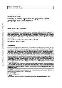
Fig.l(a) Typical C-V characteristics at 300K for n-Si Schottky diode before and after iradiation with various doses of Ar' ions.(b)Apparent carrier concentration profile obtained of curves of(a) RESULTS AND DISCUSSION Figure I(a) shows a typical 1/( 2 vs. V plot at room temperature for unimplanted and Ar' ion implanted samples with two ditherent doses. As expected for unimplanted samples, the curve is linear in the measured voltage range indicating uniformity of shallow dopant concentration. However, for implanted sample a linear region (A) occurs at high voltage and a nonlinear or flatter region (B) occurs at lower voltages . The nature of the curves are qualitatively similar for both samples irradiated with low dose (5 x 10 3 cm-2 ) and high dose (I x 1014 cm2 ) of Ar' ions. As depletion width (W) is proportional to l/C, a larger W for implanted sample compared to unitnplanted sample. Moreover, for high dose implanted sample zero bias depletion width is larger compared to low dose case. Fig. lb. shows the apparent carrier concentration as a function of width of the depletion region deduced from standard analysis of slopes of the curves in Fig. I a. The sharp rise in concentration profile is due to presence of a flat region in C-V. This feature is an artefact due to large trap density in a region of depeletion layer. TRIM simulatons predict the range of the ion to be 1.23Lýtm with no significant damage beyond 1.5ýtm. Note that the edge of lie depelion layer is at distnaces much larger from the surface than predicted by TRIM simulations. This was l6otnd to be a characteristic feature of highly damaged samples using heavy oi0ns.
404
The fact that the unusual features in C-V are indeed controlled by trap dominated regions within the depeltion layer become clear from Fig.2(a). which shows hysteresis behaviour of C-V depending on both direction and rate of voltage sweep. The C-V characteristic is identical for Voltage sweep rae 34
2.7K
Ar+:5x10
1 0.17V/s 2: 0.15 V/s
3: 0.10V/s
44: 0.07 V/s
32
10-6