Paper presented at the "VIII Congresso SATT", Como, 1-4 October 1996. (**) Permanent address: Dto. de Fisica, CNEA, Av. Libertador 8250, (1429) Cap. Fed.,.
IL NUOVO CIMENTO
VOL. 19 D, N, 8-9
Agosto-Settembre 1997
Fabrication of step-edge structures on R-plane sapphire using a selective wet etch process (*) p, LEVY (**), S. NICOLETTI, L. CORRERA, M. CERVERA (***), M. BIANCONI F. BISCARINI, F. CORTICELLI and E. GABILLI CNR-/stituto LAMEL - via Gobetti 707. 40729 Bologna. Italy (ricevuto il 18 Gennaio 1997; approvato il 22 Aprile 1997)
Summary. - With the aim of using some well established techniques in the planar tecnology of silicon for the fabrication of high- Tc grain boundary based junctions, we investigated a process suitable for the realisation of step-edge on R-plane sapphire substrates. Step-edges were prepared by exposing a photolitographically defined area to Ar+ ion implantation. The damaged area was selectively removed by different wet etching processes. With this technique we were able to produce 150 nm height steps, 30°-45° slope. The surface roughness on both sides of the step was the same as that of the virgin sustrate. The influences of dose, angle of implant, etch rate and related main feature of the process are discussed.
PACS. 74.76 - Superconducting films. PACS 01.30.Cc - Conference proceedings.
1. - Introduction
As demostrated in last years, step-edge technique emerges as a viable way to fabricate YBaZCu307 _ t....u....~______j
o
50
100
150
200
Depth (nm)
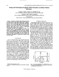
Fig. 1. - a) Defective fraction (normalized to the amorphous material value) as a function of depth for samples A and B. b) Etching rate as a function of depth for samples A and B. using Aluetch. beam. Therefore, the self annealing process makes the damage profile to go deeper [10] into the sample, as the dose is increased.
2"2. Selective etching. - After implantation, samples were wet etched using H 3 P0 4, Hz S04 and Aluetch (4 H 3 P0 4 + 4 CH 3 COOH + HN0 3 + Hz 0) at 200°C. Since damaged material is removed faster than the virgin one, a step forms at the edge of the areas protected by the resist during ion implantation.
1392
P. LEVY. S. NICOLETTI. L. CORRERA. M. CERVERA. ETC.
160 140
E 120 I::
~
..c: .... 100
c.. Q)
"C
80
---a-- sample A
60
---e- sample B
40 20
a)
160 140 120 ~
E
100
I::
~
..c: ....c.. Q)
80
"C
60
-O-AluClch
La
40
-/:,.- H 2 SO 4 ~\l-H3P04
V?/:,.
J¢.t:
20
b)
0 0
50
100
150
200
time (min)
Fig. 2. - Height of the step as a function of etching time. a) for samples A and Busing H 3 P0 4 as etchant; b) for H 3 P0 4. Aluetch. and Hz S04 etchants. at fixed dose.
In fig. 2a,b we report the etched depth as a function of the time for different doses and etchants. In fig. 2a, different saturation levels were obtained for each dose, related to the amount of generated damage. Figure 2b reports the etch features for the reactants used, at a given implant dose. Different etching rates were observed related to distinct mechanisms of material removal. Rate V5. depth for one reactant (Aluetch) is reported in fig. 1b for comparison with the corresponding defective fraction, showing a correlation with the RBS data.
FABRICATION OF STEP-EDGE STRUCTURES ON R-PLANE SAPPHIRE ETC.
1393
Step-edges were obtained faster when H 3 P0 4 was used, due to the same oxidation state displayed by P and AI. The etching reaction for Hz S04 involves formation of intermediate compounds, which slows overall related kinetic.
2'3. Step characterization. - As the angle formed by the step is a critical parameter in step-edge Josephson junction's transport properties, we performed both SEM and AFM measurements along the obtained steps. Figure 3 reports the SEM image of two 150 nm height steps, corresponding to a corner facing the ion beam during the implantation. The maximum extension of the border can be roughly evaluated to be around 500 nm, giving 30° as average slope of the step. On the other hand, the slope appears to be not constant along the step. Observation of the opposite sides of the square showed wider steps, evidencing the effect of the implantation angle on the final slope. Measurements of the step's slope were performed by AFM using a 50 nm probe. Main features of the etched steps are reported in fig 4a,b. The shadow effect due to the 8° angle between the beam and the normal to the surface produces different edges, respectively shown in 4a and 4b. From the evaluation of the slope through derivative analysis, it results that non-shadowed edges have a maximum slope of about 45°, whereas shadowed edges have a maximum slope lower than 25°, and extend more than 500 nm. These results well agree with the SEM observations previously described. Also, as observed from AFM results (not shown), the sharpness of the step is proportional to the etch rate. Moreover, as the etch continues after reaching the saturation regime, rounded corners and lower slopes appear. A noticeable feature of the whole process is that roughness is similar on both sides of the step. This effect can possibly be ascribed to the high resistance of crystalline sapphire to chemical etching.
Fig. 3. - Scanning Electron Microscopy image of a 150 nm eight step-edge (non-shadowed sides).
1394
P. LEVY. S. NICOLETTI. L. CORRERA. M. CERVERA. ETC.
1.0 150
0.8 0.6
,....... 100 S
C>
N
t>
=
0.4
'-' N
50
>
~ C>
" "
:'
=
'-' N
" "
-0.6 >