Fast and Accurate Thermal Modeling and Optimization for Monolithic 3D ICs Sandeep Kumar Samal† , Shreepad Panth† , Kambiz Samadi§ , Mehdi Saedi§ , Yang Du§ , and Sung Kyu Lim† †
School of ECE, Georgia Institute of Technology, Atlanta, GA § Qualcomm Research, San Diego, CA
[email protected],
[email protected] ABSTRACT In this paper, we present a comprehensive study of the unique thermal behavior in monolithic 3D ICs. In particular, we study the impact of the thin inter-layer dielectric (ILD) between the device tiers on vertical thermal coupling. In addition, we develop a fast and accurate compact full-chip thermal analysis model based on non-linear regression technique. Our model is extremely fast and highly accurate with an error of less than 5%. This model is incorporated into a thermal-aware 3D-floorplanner that runs without significant runtime overhead. We observe up to 22% reduction in the maximum temperature with insignificant area and performance overhead.
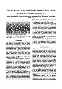
Handle Bulk + Die1 (75 µm)
Handle Bulk (75 µm) Ac!ve
M1
M1 Tier 1
Tier 1
M6 Bonding Layer (2.5um BCB)
M6 ILD (100nm SiO2)
Die Substrate (~30 µm)
Tier 0
MIV Tier 0 M6
TSV M6
Categories and Subject Descriptors B.8.2 [Performance and Reliability]: Performance Analysis and Design Aids
Keywords Monolithic 3D; Thermal; Modeling; Optimization
1. INTRODUCTION Recently developed monolithic 3D integration technology [1] enables sequential integration of device layers in contrast to bonding of fabricated dies. Monolithic 3D integration uses nano-scale monolithic inter-tier vias (MIVs) to connect the vertical device layers. MIVs are similar to regular metal-layer vias and their corresponding capacitance and area values are negligible compared to those of TSVs that are micron-scale. This allows the use of many such MIVs for vertical connections which yields in significantly higher integration density than that of TSV-based 3D ICs. Monolithic 3D ICs can overcome the shortcomings of TSV-based 3D ICs; however, one major concern with 3D ICs in general is the increase in power density which leads to high temperature values. The reduction in footprint area effectively increases the power density by the same factor. Even if we achieve power reduction by going 3D, the increased power density affects the temperature, This work is supported by Qualcomm Research. Permission to make digital or hard copies of all or part of this work for personal or classroom use is granted without fee provided that copies are not made or distributed for profit or commercial advantage and that copies bear this notice and the full citation on the first page. Copyrights for components of this work owned by others than ACM must be honored. Abstracting with credit is permitted. To copy otherwise, or republish, to post on servers or to redistribute to lists, requires prior specific permission and/or a fee. Request permissions from
[email protected]. DAC’14, June 01 - 05 2014, San Francisco, CA, USA Copyright 2014 ACM 978-1-4503-2730-5/14/06 ... $15.00. http://dx.doi.org/10.1145/2593069.2593140.
monolithic 3D IC
TSV-based 3D IC
Figure 1: 2-tier 3D IC layer structure (heat sink on top) of Monolithic 3D IC vs TSV-based 3D IC especially in the layers away from the heat sink or other equivalent cooling features in modern miniaturized electronics. Therefore, importance of thermal-aware design methodologies become more critical in 3D ICs. The major bottleneck of considering thermal aspect within the physical design process is the huge runtime required for accurate temperature analysis. The inclusion of such detailed analysis within the design process is not practically feasible. Attempts have been made to develop accurate temperature evaluation models to be included within the chip design process. The use of compact resistive thermal grid network to estimate the temperature profile of a chip has been studied [2]. They estimate the temperature during the floorplanning process and insert whitespace for dummy vias. The calculation of resistive network solving still consumes some runtime and the insertion of whitespace increases the area further, diminishing the 3D IC benefits. They report 56% reduction in temperature but with a large area increase of 21%. The optimization of silicon area is important in 3D ICs along with the temperature rise and we cannot sacrifice too much area for temperature improvement. The modeling of temperature based on total leakage power dissipation and its use in the tier-planning of similar layout processor chips has also been studied [3]. Another work uses the 3D overlap estimation along with power density calculations for thermal-aware planning [4]. All these methods are either targeted for TSV-based 3D IC design or incur extra runtime and area or use indirect methods of thermal analysis. None of the works address monolithic 3D ICs which interestingly exhibit different thermal behavior due to their layer structure. In this work (1) We study and explain the thermal characteristics of monolithic 3D ICs for the first time with comparison to TSV-
bottom die
top die
Table 1: The different materials used in the layers, their thermal conductivities and vertical thicknesses Thermal Vertical Conductivity (W/m-K) Thickness Monolithic Silicon 141 75µm SiO2 1.38 100nm TSV-based Silicon 141 75µm Silicon 141 30µm BCB 0.29 2.5µm Copper 401 30µm Solder 50 2.5µm
Layer/Structure Material Handle Bulk ILD (Inter-tier) Handle Bulk Die0 Substrate Bonding Layer TSV TSV-bump
floorplans
based 3D ICs.(2) We identify the factors affecting temperature and develop a very fast and accurate non-linear regression based temperature evaluation model for monolithic 3D ICs. This is first work on thermal modeling for monolithic 3D ICs.(3) We use our model to carry out thermal-aware 3D floorplanning and show significant reduction in maximum temperature with minimal or no area and performance overhead.
thermal maps for monolithic 3D IC
2. NEW THERMAL ISSUES 2.1 Monolithic 3D Integration A typical two-tier monolithic stackup is shown in Figure 1 in a flip-chip configuration. The first set of transistors closer to the handle bulk are processed with standard SOI process and make up Tier 1. A thin inter-layer dielectric (ILD) is deposited over the metal layers for growing the next device layer. This device layer along with the metal layers make up the other tier (Tier 0) of the 3D stackup. The transistors in these layers are processed with low temperature process (