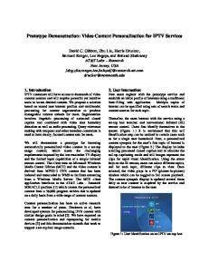
point-to-point shuffle link pattern across a multichip smart pixel array. A mirror is used to .... properties of the interconnection system with active devices. ... multichip array scenario similar to what will be encountered ... from a central motherboard before each test. .... used for the prototype demonstration is shown in figure 3.
J. Opt. A: Pure Appl. Opt. 1 (1999) 1–5. Printed in the UK
PII: S1464-4258(99)97933-3
FAST-Net optical interconnection prototype demonstration M W Haney†, M P Christensen†, P Milojkovic†, J Ekman‡, P Chandramani‡, R Rozier‡, F Kiamilev‡, Y Liu§, M Hibbs-Brenner§, J Nohava§, E Kalweit§, S Bounnak§, T Marta§ and B Walterson§ † George Mason University, Fairfax, VA 22030, USA ‡ UNC Charlotte, Charlotte, NC 28223, USA § Honeywell Technology Center, Minneapolis, MN 55418, USA Received 8 September 1998, in final form 6 November 1998 Abstract. The first prototype of the free-space accelerator for switching terabit networks
(FAST-Net) program is described. The optical interconnection module consists of an array of matched high-resolution, wide-angle ( f /1.1) imaging lenses that effect a global point-to-point shuffle link pattern across a multichip smart pixel array. A mirror is used to fold the shuffled links back onto the array to facilitate single-plane multichip packaging and simplified opto-mechanical alignment. The test system incorporates several monolithically integrated two-dimensional arrays of vertical-cavity surface-emitting lasers (VCSELs) and photodetectors (PDs) in the multichip plane. In initial experiments the prototype showed good overall optical efficiency and sufficient channel separation for VCSEL/PD arrays with pitches as small as 100 µm. These results suggest that high bisection bandwidth optical free-space interconnection fabrics are feasible for high-throughput switching and multiprocessor applications. Keywords: ???
1. Introduction
Highly interconnected multiprocessor systems are now performance limited by the backplane interconnection bottleneck associated with planar interconnection technologies. Smart pixel throughput capabilities are projected to exceed 1 Tbit s−1 cm−2 [1] and offer the promise of overcoming the bottlenecks of planar technologies for many types of interconnection-limited multiprocessor problems. Systems which use smart-pixel-based freespace optical interconnects (FSOI) provide two general dense interconnection capabilities: intelligent parallel data transfer and intelligent parallel data interchange. Optical imaging provides a high-throughput approach to linking smart pixel planes for data transfer. In this case, the high I/O density of smart pixels may provide a power consumption and size advantage over electronics [2, 3]. For data interchange, FSOI provides the additional ability to perform the data partitioning and interleaving useful in spacevariant link interconnection patterns such as the perfect shuffle (PS) [4], which are inherently difficult to implement in planar interconnection technologies. Such patterns are characterized by high bisection bandwidth (BSBW) [5]. In multiprocessor architecture design, there is a direct tradeoff between minimum BSBW and latency in a network. It is therefore generally desirable to implement networks with the largest minimum BSBW that can be achieved 1464-4258/99/000001+05$19.50 © 1999 IOP Publishing Ltd
practically to solve a given problem. The ability of optical elements to interconnect large arrays in space-variant patterns, without crosstalk in the medium, suggests that FSOI techniques are particularly promising for problems with high BSBW. For problems with greater than ∼1 Tbit s−1 BSBW (i.e. greater than the capabilities of a single chip) free-space optical interconnects have a marked advantage [6, 7]. Therefore, globally interconnected multichip smartpixel-based architectures have the potential to reap the full benefits of FSOI. The free-space accelerator for switching terabit Net works (FAST-Net) project, sponsored by the US Defense Advanced Research Projects Agency, is tasked with applying FSOI and smart pixels to real-world multiprocessor interconnection problems [8]. The FAST-Net concept is intended for application to a general class of interconnectionlimited (i.e. high-BSBW) multiprocessor problems, such as high-throughput switching and image processing, which are characterized by severe interconnection constraints on performance. The general applicability of the FAST-Net concept stems from its combination of global multichip optical interconnections with local electronic routing within each smart pixel chip. This concept has been shown to provide an interconnection fabric with the flexibility to implement any permutation pattern with low latency [9]. This paper reviews the initial FAST-Net optical interconnection prototype and its preliminary evaluation 1
M W Haney et al
with two-dimensional (2D) arrays of monolithically integrated high-bandwidth vertical-cavity surface-emitting lasers (VCSELs) and photodetectors (PDs). The prototype and its key electronic and optoelectronic elements are described in section 2. The results of the preliminary characterization of the prototype are presented in section 3. The characterization focuses on two issues: (a) the ability of the global interconnection optics to reliably separate closely spaced VCSEL/MSM channels across the wide fields of view of the FSOI system, and (b) the overall point-to-point (VCSL to PD) optical efficiency of the system. Section 4 is a conclusion which summarizes the encouraging results and describes how the experiments reported here will lead to the planned next phase of FAST-Net development. 2. Experimental prototype
A distinctive feature of the FAST-Net concept is that all smart pixels are distributed across a single multichip plane. This plane is connected to itself via an optical system that consists of an array of matched lenses (one for each smart pixel chip position) and a mirror [10]. The optical interconnect system implements a global point-to-point shuffle pattern. The interleaved 2D arrays of VCSELs and PDs in the prototype are arranged on a clustered self-similar grid pattern [11] to facilitate packaging and optomechanical alignment. In previous research, a photolithographic etched mask was employed to simulate a multichip VCSEL/PD array. That effort proved that the approach achieves the interconnection density and alignment accuracy required for the FAST-Net approach [10]. The overall goal of the first FAST-Net prototype demonstration is to replace the mask with actual VCESL/PD arrays and test the overall optical properties of the interconnection system with active devices. The ultimate system will integrate optical ICs on an MCM with a placement accuracy of ∼10 µm. As described in section 2.3 below, the first prototype emulates precise MCM chip placement by mounting each optical array IC on its own separately positioned daughter card. The system allows the alignment techniques developed previously with a passive array to be refined in an active integrated emitter/receiver multichip array scenario similar to what will be encountered in the final MCM system. The FAST-Net prototype system brings together three technology areas. CMOS driver, receiver and control electronics are combined with GaAs VCSEL/PD arrays in an optomechanical interconnection module for this evaluation system. The following sections detail these three elements. 2.1. Smart-pixel emulator boards The smart-pixel multichip module is emulated by utilizing printed circuit boards (PCBs) with discretely packaged VCSEL/PD arrays, CMOS VCSEL driver ICs, CMOS receiver ICs and FPGAs. The eventual bump-bonded integrated smart-pixel chip will contain all the CMOS circuitry and VCSEL/PD array within one hybrid package. In the present demonstration, these components are located on small daughter cards that are positioned in the optical module. The discrete nature of these separately packaged 2
Figure 1. Photograph of a CMOS VCSEL driver chip with a
pseudo-random test pattern generator. The left-hand edge of the chip contains 10 VCSEL driver channels.
parts causes a limitation in the bandwidth that can be controlled externally. This limitation is somewhat overcome by placing a programmable control FPGA on each daughter card that performs the required instructions. Test patterns for the VCSEL arrays are loaded onto each daughter card from a central motherboard before each test. Additionally, daughter cards are programmed to transmit selected receiver outputs back to the motherboard for display. In this fashion, all point-to-point optical links in the global multichip shuffle pattern can be evaluated individually and at a bandwidth that is not limited by board-to-board control interface limitations. Although the drivers and receiver circuits were designed for high-speed operation, they were operated at a slow speed for the experiments described in this paper. Figure 1 is a photograph of the VCSEL driver/test chip, fabricated in 0.5 µm CMOS. It contains 10 asynchronous channel drivers, with CMOS inputs and current-mode outputs. Modulation and bias are adjustable over a wide range (20 mA for bias and 40 mA for modulation). The chip can also operate in self-test mode. In this mode, a pseudorandom data stream is generated on-chip and transmitted to the VCSEL array. An adjustable on-chip clock generator (150 MHz to 1 GHz) is used to synchronize the operation (in self-test mode). Thus, the chip can test the high-speed operation of the VCSEL device array without requiring highspeed signal generation equipment. In the test system, the VCSEL drivers had sufficient current to drive four VCSELs simultaneously. Consequently, for evaluation purposes, four VCSELs were driven in parallel by each channel of the chip. This simplified the layout of the daughter card, as otherwise three additional driver ICs would have been necessary per daughter card. The self-test circuitry
FAST-Net optical interconnection prototype demonstration
Figure 3. FAST-Net prototype evaluation system.
Figure 2. Photograph of a 2D integrated VCSEL and MSM
photodetector array chip. (This figure can be viewed in colour in the electronic version of the article; see http://www.iop.org)
of this chip provided a convenient bit pattern for optical link analysis. 2.2. VCSEL/MSM detector arrays The VCSEL structure is grown by MOCVD. First, a VCSEL bottom mirror stack is grown on top of a semi-insulating GaAs substrate, followed by an n-type doped contact layer, and then multiple quantum well active layers and a standard p-type top mirror stack are grown. A 1.5 µm cap layer of undoped GaAs is grown on which the MSM is fabricated. The Schottky metal used for the photodetector fingers is WSix . A selective wet chemical etch is used to remove the GaAs cap layer in the region where the VCSELs are processed. Next a p-ohmic metal deposition and gain-guide implantation defines the VCSEL active window. A precisely controlled dry etch process is used to access the n-contact layer. An n-ohmic metal deposited on the n-contact layer, followed by a device isolation implant, a polyamide for passivation and inter-metal insulation, and finally an interconnect metal. The integrated VCSELs, which has both p- and ncontacts on top of the semi-insulating GaAs substrate, have similar device characteristics as those VCSELs made on n+ substrates. A typical device has a threshold current of 3.5– 4 mA, and threshold voltage of 1.7–1.8 V, a maximum output power of over 8 mW at 850 nm for a 15 µm diameter device, and a small-signal bandwidth of over 9 GHz. The integrated MSM photodetector has a typical responsivity of 0.3 A W−1 (without AR coating) at 850 nm. The rise time of the detector, measured using wafer-level probing was measured to be approximately 150 ps. Figure 2 is a microphotograph of the 2D VCSEL/MSM integrated array chip designed for the FAST-Net free-space optical interconnect module. In this 2D array device, there are a total of 32 VCSELs, each with an aperture window of
10 µm, and 36 MSM photodetectors, each with a 50 µm square active region. All devices have coplanar contacts that are routed to 88 bonding pads at the periphery of the chip. The pattern of optical I/O shown in figure 2 is a grid pattern designed to optimize the optical interconnection in terms of chip placement and lens packaging [11]. In this pattern, parallel optical links between chips are clustered in the same physical region on the chip. The cluster spacing on the arrays is matched to the lens array in such a way as to effect an image mapping of each cluster onto a corresponding cluster of another chip in the 4 × 4 array. The four detectors, which break the repeating pattern (located in the corner clusters of each chip), are for alignment and crosstalk analysis purposes and are not intended for data communication. The side of each square cluster measures 140 µm; thus the centre detectors in the corner clusters are about 100 µm from the other elements of their clusters. These dimensions are typical for projected high-density VCSEL arrays. In turn, each cluster (consisting of two VCSELs and PDs) is spaced at 800 µm centres within the chip. This 4×4 optical I/O pattern is self-similar to the 4 × 4 lens array/chip pattern [8, 11] of the optical interconnection system. 2.3. Optomechanical interconnection system integration A photograph of the optomechanical interconnection module used for the prototype demonstration is shown in figure 3. The module comprises 16 lenses fixed in a common plane and a mirror positioned above the lenses to fold the system back upon itself. The module design was based on the sliding Banyan passive interconnect demonstration system [10]. The 4 × 4 lens arrays measures about 10 × 10 cm2 in its plane. The VCSEL/PD plane resides under the lens array, positioned such that the elements are in the back focal plane of the lenses. The folding mirror is positioned approximately 15 cm above the VCSEL/PD plane, indicating that the total free-space path length for any of the VCSEL/PD links is about 30 cm. In the experimental prototype only the smart-pixel chip positions located at the four corners of the multichip plane were populated with VCSEL/PD arrays, due to the size of the discretely packaged optical arrays. Although not fully populated, this arrangement permitted the full evaluation of the optical interconnection system since it simultaneously encompassed the shallowest and steepest 3
M W Haney et al
beam angles necessary. The shallowest beam angles occur when a VCSEL cluster is positioned to link to its own local PD cluster through a single lens. The steepest angles occur for those VCSELs on one corner of the array that are linked to PDs on the chip located on the diagonal corner of the array. The angles between the VCSEL beam and the optical axis of the lens in this wide-angle case exceeded 20◦ . Four VCSEL/PD arrays, mounted in pin-grid packages are each attached to a daughter card containing the required drivers, receivers and FPGA circuitry, as described above. Each daughter card, in turn, is mounted on a micropositioning assembly with five degrees of freedom x, y and three angles) to emulate the pick-and-place positioning of the flip-chipped hybrid ICs on the eventual MCM module. A master controller, used to activate the VCSELs and provide an indication of the detectors being triggered, resides on the motherboard (not shown). Ribbon cables connect the four daughter boards to the motherboard. A lens is positioned above each VCSEL/PD array in a lens holder which afforded a positioning adjustment range of about 200 µm in the plane of the lenses. This lens positioning arrangement provides enough flexibility to compensate for the specified machining tolerances of the lens barrels. The single backplane approach of FAST-Net removes the excess degrees of freedom (DoF) that would be present between each pair of planes of a multiplane architecture. The FASTNet approach minimizes the DoF necessary to align the FSOI and facilitates an automated alignment procedure—critical for the eventual manufacture of such optoelectronic systems. The overall optical I/O pattern is divided into 16 sections, each belonging to one optoelectronic IC, with a lens above it. As shown in figure 2, each IC has 16 sections corresponding to a cluster of optical I/O communicating with another optical IC of the array. The clusters contain four parallel links between the two optical ICs, thereby allowing the analysis of cross-talk in a dense (140 µm separation) optical interconnection module. 3. Results
Preliminary measurements of the optical properties of the FAST-Net prototype were carried out using elements of the four VCSEL/PD arrays described above. The key aspects to be characterized were spatial crosstalk (between closely spaced VCSEL/PD pairs that are in the same cluster) and optical efficiency. The following sections describe these measurements. 3.1. Crosstalk All inter-chip link varieties were verified using the prototype system. This validation was carried out by simultaneously linking closely spaced VCSEL pairs (spaced at 140 µm) with corresponding detector pairs on chips positioned across the simulated MCM. The receiver circuits included adjustable threshold circuitry to trigger a digital indication of light detection. The measurements focused on the most extreme, corner-to-corner, VCSEL/detector links that stressed the optical system to the highest possible extent because of the steep angles. All of the links achieved sufficient optical 4
Figure 4. Optical power drop through the system
resolution, registration and efficiency to interconnect active interleaved arrays of VCSELs and photodetectors in a system without crosstalk. The absence of measurable crosstalk is attributed to the excellent light confinement (resolution) of the optical system. As will be described in the next section, most of the light energy that reaches a detector is captured by the 50 µm photodetectors, and only a small fraction of the light is lost at the boundaries of the photodetectors due to resolution imperfections. In the most stressing crosstalk measurements a VCSEL spot was positioned to trigger the centre detector in one of the corner clusters on an array. In this case, adjacent detectors, located only 100 µm away were not triggered by residual light from the focused central VCSEL beam. These optical crosstalk results suggest that the FASTNet module should maintain extremely low bit-error rates (BERs). 3.2. Optical efficiency analysis The optical efficiency of the system is an important characteristic in determining eventual system performance. For the FAST-Net prototype, the optical transmission efficiency for a given VCESL beam was measured using a calibrated large-area detector repositioned to three locations: just after the first lens, just after the mirror reflection and in the back focal plane of the second lens. Two types of measurements were made in the back focal plane of the second lens: one with the broad-area detector and one with the broad area detector masked with a 50 µm diameter pinhole. The pinhole was used to simulate the 50 µm MSM PD aperture and thereby give an estimation of the amount of light power captured by the MSM PD in the prototype system. A single VCSEL was used throughout the measurements in order to provide uniformity of results. VCSEL optical power was varied between 90 µW and 1.7 mW. Measurement results were repeatable and stable. Figure 4 shows a typical variation of the normalized VCSEL beam power as it moves through the prototype system. The results show that optical power is reduced after transmission through each lens and reflection from the mirror, as well as at the pinhole. Note that the lenses and mirror contribute significant reflection and transmission loss because they are off-the-shelf components, not optimized for the VCSEL wavelength. This is consistent with the fact that the prototype
FAST-Net optical interconnection prototype demonstration
uses multielement lenses (13 surfaces), and that each lens surface has ∼ 97% transmission at the VCSEL wavelength. The mirror accurately reflects ∼ 80% of the incident power; the loss is due to scattering, absorption or transmission as the mirror was not designed for the wavelength of interest. The pinhole measurements indicate that about 85% of the light that reaches the detector is collected by the circular 50 µm diameter pinhole. This result is an indirect proof that the relevant aberrations of the optical system are small enough that their effect on the overall light budget is negligible. As shown in figure 4, the light captured by one of the MSM PDs is estimated to be 34% of the light emitted by the VCSEL. Very similar results were observed regardless of the VCSEL power used in measurements. The results suggest that simply optimizing the lenses (with antireflection coatings) and mirror for operation at the VCSEL wavelength will result in minimal optical losses. 4. Conclusions
The successful incorporation of 2D monolithically integrated arrays of VCSELs and PDs into the FAST-Net FSOI module is a significant step toward the application of smart pixels to multiprocessor interconnection problems. The encouraging results of the characterization of the prototype suggest that high-density multichip VCSEL-based global optical interconnections, with low optical losses, are feasible. The next step planned in the development of the FAST-Net concept is the incorporation of true smart pixels in which the VCSEL/PD arrays are bump-bonded to the CMOS driver and logic circuitry. This will allow a higher density of optoelectronics, because the interconnections will not be limited to the edge of the chips, and higher-speed operation, owing to the low electrical parasitics of bump-bonded interconnections. Other future work includes the custom optical design of single-element lenses for the FAST-Net lens array that will allow the overall optical efficiency to approach 100%. As integrated VCSEL-based smart-pixel technology
matures, the FAST-Net approach will be ready to exploit it to provide a path to terabit s−1 BSBW multiprocessor systems. Acknowledgments
This work is supported by the US Defense Advanced Research Projects Agency through the US Air Force Wright Laboratory under contract no F33615-97-C-1054. References [1] Nakahara T, Matsuo S, Fukushima S and Kurokawa T 1996 Performance comparison between multiple-quantum-well modulator-based and vertical-cavity-surface-emitting laser-based smart pixels Appl. Opt. 35 no 5 [2] Feldman M R et al 1989 Comparison between electrical and free space optical interconnects for fine grain processor arrays based on interconnect density capabilities Appl. Opt. 28 3820–9 [3] Miller D A B 1989 Optics for low-energy communication inside digital processors: quantum detectors, sources and modulators as efficient impedance converters Opt. Lett. 14 146–8 [4] Stone H S 1971 Parallel processing with the perfect shuffle IEEE Trans. Component Packag. Manuf. Technol. C 20 [5] Leighton F T 1992 Introduction to Parallel Algorithms and Architectures; Arrays, Trees, Hypercubes (San Mateo, CA: Morgan Kaufmann) [6] Haney M W and Christensen M P 1996 Fundamental geometric advantages of free-space optical interconnects Proc. MPPOI’96 [7] Haney M W and Christensen M P 1998 Performance scaling comparison for free-space optical and electrical interconnection approaches Appl. Opt. to be published [8] Haney M W et al 1998 FAST-Net optical interconnection prototype demonstration program Proc SPIE 3288 194–203 [9] Christensen M P and Haney M W 1998 Two-bounce optical arbitrary permutation network Appl. Opt. 37 2879–85 [10] Michael R R, Christensen M P and Haney M W 1996 Experimental evaluation of the 3D optical shuffle interconnection module of the sliding Banyan network J. Lightwave Technol. 14 no 9 [11] Haney M W 1993 Self-similar grid patterns in free-space shuffle/exchange networks Opt. Lett. 18 no 23
5