Fast Transient Response with Combined Linear-Non-Linear Control Applied to Buck Converters A. Barrado, R.Vizquez, A. Lizaro, J. Pleite, E. Olias. Universidad Carlos III de Madrid Departamento de Tecnologia Electr6nica Grupo de Sistemas Electrhicos de Potencia CButarque 15,28911, LeganCs, Madrid, SPAIN Tel.: 34-1-6249188 FAX: 34-1-6249430 E-mail:
[email protected] Abstract- Nowadays, one of the main challenges for power supplies designers is to feed last generation of microprocessors and DSPs, since they require high current slew rates together with low output voltage. In this paper, a novel control technique is presented to help the designers to comply with the current requirements. The proposed combined Linear-NonLinear Control (LnLC) increases significantly the capability of a conventional linear control to reduce the recovery time of the output voltage drop produced when a load current step occurs. Experimental results have been obtained for two cases: a synchronous rectifier buck converter, with a conventional voltage loop and the same converter with the novel LnLC. The comparison of these experimental results shown that with the new control the recovery time of the output voltage is reduced.
I. INTRODUCTION. Microprocessors and DSPs are widely used in many commercial and industrial applications. These components have been improved from the point of view of clock frequency, integration and applicability. However to get theses improvement, it has been needed to reduce the operation voltage even without reducing the power consumption. In general, five are the main requirements to feed last generation microprocessors and DSPs [1-41: Low output voltage: 1 to 3.3 V. Output voltage tolerance: f 2% (60mv for 3 V output voltage, 30 mV for 1.5 V). High load current: 1 to 50 A. High current slew rate: up to 5 Nns. Reduced converter size & improved converter efficiency. By means of the synchronous rectification technique, low output voltage has become feasible, [5-61. However the requirement of size and efficiency for load currents up to 50 A has led to the limit the capabilities of synchronous rectifier buck converters. Therefore, new topological changes should be proposed to improve these features. Nowadays, two main trends appear to feed microprocessors, those which use high input voltage (3672V), [7-91 and those which use low input voltage (12 5V), [3,4,10,11]. This paper is focused on low input voltage.
0-7803-7262-X/02/$10.00 ' 2002 IEEE.
Nevertheless, the main problem that the DCDC converters must face up is the high current slew rate imposed by microprocessors and DSPs.
I
Io
I
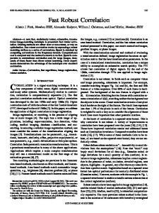
Parasitic dominant: ESR, ESL, Land R
I
-
Filter (L, C) and control
Recovery Time
Fig. I : Influence on voltage drop.
When a positive or negative load current step occurs a transient appears in output voltage of the converter. It is necessary to reduce the spike and the duration of the output voltage drop. A detailed analysis about the spikes and duration of the voltage drop and its relation with the parasitics of bulk and decoupling capacitors, packaging etc., can be found in [12]. In Fig. 1, just a simplified scheme is presented which will be explained in the principle of operation. In this way, an improved converter bandwidth and bigger output capacitors has been used to avoid this effects, but they are not enough with the current requirements. Therefore new strategies must be developed. Many of the recent references propose topological changes [3,4,10,11], however, a control improvement is proposed in this paper, the novel Combined Linear-NonLinear Control (LnLC), Fig. 2, which could aid to meet the second and fourth above requirements: output voltage tolerance for high current slew rate. If on a conventional buck converter, as only variation, the LnL Control is added, a significant reduction of the output voltage recovery time is achieved. Furthermore, this technique not only can be applied alone, it can be applied in addition to topological improvements to obtain better dynamic performances. The principle of operation and experimental results to check the proposed idea are presented in this paper.
1587
set the multiplexer selection input (UNL) to 0 and the
II. OPERATTON PRINCIPLE. For any buck converter controlled by means of a conventional linear voltage loop, when a positive load current step occurs, a "notch" appears in output voltage, Fig. 1. First of all, a negative voltage edge is produced due to the bulk and decoupling capacitors performance (output capacitor equivalent series resistance, ESR, and equivalent series inductance, ESL) and the parasitic inductances of the connection. After that, the output capacitor begins to discharge.
linear control regulates the converter. But, if output voltage exceeds the limits, the input L/NL is set to 1 and the converter results under a non-linear control (Fig. 4.d). The Duty Cycle Saturation-Reset Logic block force to 1 the duty cycle if LT is surpassed and set the duty cycle to 0 if output voltage is above the higher threshold, HT (see Fig. 4.c)
t'o
I
I
b
I
1
I I
D
0
;
-
Combined Linear Non Linear Control
Fig. 2: Buck
The output voltage delay to return to its nominal value (recovery time) depends basically on two factors: the first one is the inductor value (considering output voltage almost constant), the second one is the dynamic response of the regulator. In a converter with a conventional linear control, the dynamic response of the regulator depends on the evolution of the voltage of its capacitors. This evolution must be enough slow to keep up the stability of the converter. As a consequence, the duty cycle cannot vary instantaneous, imposing high recovery times. All this process is presented in Fig. 3.a. In this paper a new control method is proposed, this method combines a linear and a non-linear control. Output voltage is compared with two levels: the higher threshold (HT) and the lower threshold (LT), figures 3 and 4. In the case shown in Fig. 3.b, under a positive load current step, when output voltage drops below the LT, the duty cycle is set to 1. In the buck converter, the input voltage is directly applied to the output filter. Now, only the dynamic of the LC-R cell affects on the recovery time of output voltage. With a linear control in a buck converter when the positive load step occurs the duty cycle cannot vary quickly due to the dynamic of the regulator capacitors, then the voltage drop cannot eliminate as soon as possible. In Fig. 2 is represented a buck converter and the blocks diagram of the proposed control. While output voltage remains between the levels HT and LT (gray band in Fig. 4.b), the Threshold Logic block
1588
+ I
"GS
Fig. 3: Output voltage evolution under load current step, for linear and linear-non-linear combined control.
HT
LT
I
./ ./ ..j / . ./ .j
. j
j
.
. . j
i
j
i
:
:
Fig. 4: Multiplexer selection input (UNL), Duty cycle and output voltage evolution under load steps.
The non-linear control block operates on the output of the control circuit; therefore, the non-linear control circuitry does not modify the voltage of the regulator capacitors. These voltages only evolve according to output voltage. So, instability is not produced when output voltage returns under the level HT o LT and the linear control has to regulate the converter again (notice this detail in Fig. 4.c).
1+
...
L'.. . . . . . : , .
t : "
m.EXPERIMENTAL RESULTS.
.-.
.
-.
L
.
.
. . . .
. .
.
(L)
1
I
OUTPUT VOLTAGE MAXIMUM LOAD CURRENT STEP
I
.
.-.
-.
/?Ii
. . .. .b. . . . : . . . . . . . .../
-. -.
.
.
.
.
le
(1 00 mV/div, AC coupling). Ch2: Io, load current (20 Mdiv). Ch3: I ,
ou
7pH 10000 pF
bPUT VOLTAGE
..Ji
: :ti
F
250 kHz
OUTPUT CAPACITOR. (C)
. . . . .
I! .
.
INDUCTANCE
:
.
. .
.
SWITCHING FREQUENCY
:
. . . . . . .
i
. . . . . . . . .
2+
To obtain the experimental results, a buck converter with synchronous rectification has been built and experimentally tested. The complete specifications are listed in table 1.
:
1.5 V 16 A
1+
In order to check the performances of the combined linear-non-linear control, the buck converter prototype has been tested with both controls. Experimental results are presented for two cases: Buck converter with a conventional Linear control: BL. 0 Buck converter with the proposed combined Linear-non-Linearcontrol: BLnL.
h __
i :
i
: P., -. ............................. . . _. . . . _. .
AVO . . ... . ... . .. . . . . . . . . . .
t
1:
i ~
I I
Main system waveforms. In figures 5 and 6 it can be seen the differences between linear control and linear-non-linear control when a 16A load current step is applied on the same converter. In general, the Linear-non-linear control allows recovery times much smaller than the Linear control. In this case, this figures shown a clear improvement in the load step rise edge, however, in the load step fall edge the influence of Linear-non-linear control is not very important. This is not always thus, the obtained improvement with the linear-non-linear control respect to the linear control depends on the optimization of the buck control design, the output voltage and the load step value. In figures 7 and 8 are shown the output voltage ripple obtained with linear and linear-non-linear control for the same buck converter but when an 8A load current step is apply. In this case the obtained results shown, how the linear-non-linear control improves the rise and fall recovery time more significantly than previous cases.
Fig. 6: BLaL under a 16A load current step. ChI: AVO, output voltage npple (100 mV/div, AC coupling). Ch2: Io, load current (2OMdiv). Ch3: I , Output Current of the Buck Converter (20 Mdiv). Tune base 200 pddiv.
! I.
I.
..
:.
. . . . . .: .. . .: . .
.... . . .
:
...: . . . . . . . . . . .
. . . . . . . . . . . . .. . .. ..:. . . . . . . . . . . . . . . . . . .. . . . . . . . . . . . . . . . . . . . . . . .
I
-.
.
I,
Fig. 7: BL under an 8A load current step. Chl: AVO, output voltage ripple (100 mV/div, AC coupling). Ch2: Io, load current (20 Mdiv). Ch3: 1.w. Output Current of the Buck Converter (ZOA/div).Timebase 200 pddiv.
1589
11 I
I
. . . :. . . . :. . . . . : . . . . ; . . . ; . . . . . .; . , ; . . , _.
1
1
. . * .. , . .................... . . .
.
.& .... .. . , . , . ,
.
. : . .
. . . .
. , ,
.
..i. . . . . . . . . . . . .. . . . . . . .
I
1I I'
-
.
.
.
I
i
I ~
Fig. 9: BL ouipui voltage recovery time at load curreni rise edge. Chl: AVO,'ouiput voltage ripple (100 mV/div). Ch2: Io, load current (20MdN). Ch3. I , Ouipui Current of the Buck Converter (20 Mdiv). Time base 50 Wdiv.
Fig. 8: BLAL under an 8A load current step. Chl: AVO,output voltage ripple (100 mV/div, AC coupling). Ch2: Io, bad current (20Mdiv). Ch3: lm, Output Current of the Buck Converter (20 Ndiv). Time base 200 pddiv.
.
Output voltage recovery time comparison.
. . . :. . . .
. . :
. . .
:
.
. .: . . .
: .
. +
.