Proceedings of the 2nd COST G-6 Workshop on Digital Audio Effects (DAFx99), NTNU, Trondheim, December 9-11, 1999
FILTER IMPLEMENTATION ON SYNTHUP Jean-Michel Raczinski Stéphane Sladek Luc Chevalier CEMAMu CNET-B403 38-40, rue du Général Leclerc 92794 ISSY-LES-MOULINEAUX Cedex 9 France
[email protected] [email protected] [email protected]
2.
ABSTRACT This paper presents different implementations of digital filters on SYNTHUP, a PCI plug-in board based on FPGAs (Field Programmable Gate Arrays). The modular architecture of the board features a PCI interface, seven identical cells dedicated to computing, five FPGAs dedicated to data exchange, one cell for control and a total of 128M bytes of dual port SDRAM. The PCI interface offers bus mastering (scatter-gather DMA) for high speed data transfer between the board and the host memory. Applications are downloaded from the host via PCI into the logical resources of the FPGAs in few milliseconds. Each cell is made up of a FPGA that drives two independent 4M×16 SDRAM. It is connected to a 32 bit control bus and to an array of exchange FPGAs through a 64 bit bus. These FPGAs work as a crossbar switch. Moreover, they drive five 12 bit ports intended for communication with other boards. The paper concentrates on the implementation of FIR serial filters with distributed arithmetic which allows one FPGA to drive 48 channels in real time (48 kHz sampling rate, 16 bit data and coefficients). As the coefficients can be changed, each channel has its own filter (100 taps, adaptive filter). One can also build a 4800 taps filter for one channel.
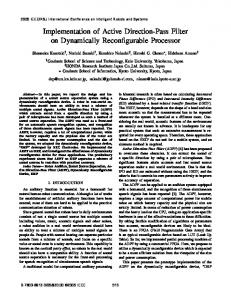
The architecture of the board has been described in a previous paper in French [1]. However, we will stress here on a few points of interest for DSP applications. exchange bus
update bus
W99-1
adress and control SDRAM A SDRAM B data
16 16
32
Figure 1. SYNTHUP cell. The basic cell is made up of a FPGA that drives two independent 4M×16 SDRAM. This allows two accesses (read and/or write) to take place simultaneously. The memory can also be configured as a plain 4M×32. When used to store data, this memory is programmed as a FIFO. control bus
PCI 9080
INTRODUCTION
SYNTHUP is a PCI plug-in board that has been designed at CEMAMu (Centre d’Études de Mathématique et Automatique Musicales) for real-time sound synthesis and can be used for general purpose digital signal processing. It is based on Xilinx FPGAs which combine the flexibility of programmable devices and the performance of a custom hardware solution. The modular architecture of the board together with the FPGA technology allows efficient implementation of parallel computationally intensive algorithms. This makes the board a good tool for implementing filters, FFTs, etc.
64
FPGA
PCI
1.
SYNTHUP
4 internal links
...
cell 7
cell 0
cell 1
SDRAM
SDRAM
SDRAM
FPGA
FPGA
FPGA
5 exchange FPGAs
external link
Figure 2. SYNTHUP architecture. The board gathers eight identical cells, which gives a total of 128 Mbytes of on board memory. Seven cells are dedicated to computing; cell 0 is intended for control and handles the PCI interface. Special attention has been paid to data exchange between the computing cells. Each cell can exchange 64 bits with the other cells through an array of five exchange FPGAs. These FPGAs
Proceedings of the 2nd COST G-6 Workshop on Digital Audio Effects (DAFx99), NTNU, Trondheim, December 9-11, 1999
work as a crossbar switch. Thanks to the FPGA technology, each bit can be programmed individually as input or output or general I/O. The exchange FPGAs are also responsible for the communication with other boards. They drive five 12 bit ports: one link is available on a 37 pin connector on the card bracket, the four others are intended for communication with other boards in the PC. Here also, each bit is programmable as input, output or general I/O with data or control functionality. The PCI interface is handled by a dedicated component from PLX (PCI 9080). It features full PCI V2.1 compliance (32 bit, 33 MHz) including 5 volts and 3,3 volts compatibility; true Plug and Play installation and configuration as well as bus mastering for high speed transfer between the board and the host memory (scatter-gather DMA). Applications are downloaded from the host via PCI into the logical resources of the FPGAs in few milliseconds. This makes the system fully re-configurable at will. This makes also the board to act as a co-processor that implement intensive calculations independently from the host. A VxD driver is available allowing access to the board under Windows 95 and 98. Next WDM version will be Windows 2000 compatible.
The FPGAs SRAM based technology allows the user to reconfigure the chip as many times as needed. Moreover, the designer implements exactly what is required for a given application through highly parameterized building blocks. He starts the design by translating the DSP algorithm into a circuit schematic using a schematic editor or by describing the algorithm with a high level language like VHDL. Then, a software environment including simulation and timing analysis helps him to control how the design is mapped and routed into the logical resources of the FPGA.
Figure 4. FPGA architecture. The devices feature a gate-array like architecture with a matrix of configurable logic blocks (CLBs) surrounded by a periphery of I/O blocks (IOBs). This regular structure holds an abundance of registers which enables a high degree of pipelining and leads to increase performance for parallel processing.
Figure 3. SYNTHUP layout. The footprint of the FPGAs (PQ240) allows us to install any component of the 4000XL or 4000XLA family, starting with 4013 (10K-30K gates equivalent) up to 4085 (75K-200K gates equivalent). It will be also possible to install 256 Mbit SDRAM instead of today’s 64 Mbit. The board works with a common 40 MHz clock. 3.
FPGA Figure 5. Simplified block diagram of XC4000XL CLB.
In the last years, FPGAs have become a new option for implementing programmable digital signal processing algorithms. On one hand, general-purpose DSP chips give a lot of flexibility as they can be programmed at will using a high level language like C. They allow fast design iterations and reduce time to market but debugging multi-processor software may turn out to be a tricky activity. On the other hand, Application-Specific Integrated Circuits (ASICs) deliver performance at the expense of high development costs, the inability to make design modification after production and a high price per chip when not manufactured in high volume. As an alternative, FPGAs offer the best of both worlds: flexibility and performance.
Each CLB includes two 4 bit look-up tables (LUT) and two 1 bit registers. A dedicated fast carry chain improves the performance of adders, accumulators, comparators and counters. For example, a 32 bit adder takes 16 CLBs and functions at 108 MHz in the 4000XLA family. Moreover, each CLB can be configured as a 16×1, 16×2 or 32×1 single port synchronous RAM or as a 16×1 dual port synchronous RAM with simultaneous read/write. This distributed RAM is a key element for DSP applications.
W99-2
Proceedings of the 2nd COST G-6 Workshop on Digital Audio Effects (DAFx99), NTNU, Trondheim, December 9-11, 1999
address x1,b x2,b
Eventually, the programmability of each IOB as input, output or general I/O with or without registers gives a lot of flexibility and allows fast data transfers between devices. FILTER IMPLEMENTATION
We will focus on Distributed Arithmetic implementations of FIR filters because they make an intensive use of look-up tables that are easily implemented in FPGAs. The response of a K taps FIR filter can be expressed as the following sum of products:
Taps 4 8 12 16 20
(1)
k =1
Where y(n) is the response at time n, xk(n) is the kth prior input data at time n and the Ak are the coefficients of the filter. We assume data and coefficients are coded on B and C bits respectively. Input data xk may be written with 2’s complement notation as follow: B −1
x k = − x k , 0 + ∑ x k ,b 2
−b
(2)
b =1
Where xk,b is a binary variable and xk,0 is the sign bit. This leads to explicitly express all product terms of equation (1) as: y(n) = − [ x1,0 • A1 + x2,0 • A2 + ... + xK ,0 • AK ] −1
+ [ x1,1 • A1 + x2,1 • A2 + ...+ xK ,1 • AK ] 2
xK,b
AK
2 A2 3 A2 + A1 4 A3 2K AK +…+ A1 2K words × A bits
8 bits 146 189 335 365 498
8 bits 12 bits 16 bits 186 226 229 269 411 487 441 517 610 722
8 bits 282 360 631 685 933
16 bits Data 12 bits 16 bits Coef. 354 428 432 506 772 914 826 968 1142 1352
Device CLBs 4013 576 4020 784 4028 1024 4036 1296 4044 1600 4052 1936 4062 2304 4085 3136
Table 1. CLB number for a parallel Distributed Arithmetic implementation of a symmetric FIR filter. On the other hand, serial implementation requires less resources (CLBs) at the expense of a limited sample rate. The B partial terms x1,b ; x2,b ; …, xK,b (b = 1, …, B) are successively sent to a single look-up table, LSB first (weight 2-(B-1)). The output of this look-up table enters a scaling accumulator (scale by ½) that will accumulate the B contributions so that one gets the final output result in B clock cycles for a non symmetric filter and B+1 cycles for a symmetric filter.
(3)
+ ... + [ x1,B−1 • A1 + x2,B−1 • A2 + ...+ xK ,B−1 • AK ] 2
Ak
A
In a fully parallel implementation, the input samples are stored in a series of registers (one register per tap) which feed a series of look-up tables. As all B bits of all K data sources address the B look-up tables, one gets the output in a single clock cycle. This is the fastest solution as it runs at the system frequency (40 MHz on SYNTHUP). But speed has its cost: a high number of CLBs. This is the classic speed – resources tradeoff. In other words, the number of taps is limited by the resources of the FPGA installed on the board. For example, an XC4028XLA (1024 CLBs) will implement a maximum of 16 taps with 16 bit data and coefficients.
K
y ( n ) = ∑ Ak • x k ( n )
xk,b
data
0 0 1 A1
Figure 7. Look-up table addressing and content.
Figure 6. Simplified block diagram of XC4000XL IOB.
4.
A1 A2
Taps 8 16 32 64 80
−( B−1)
Each term within the brackets involves only one bit of the input data with all the bits of the coefficients. This allows to construct a look-up table that can be addressed by the same bit of all input variables. This look-up table holds all the additive combinations of the coefficients: 2K elements of A = C + p bits when 2p-1 < K ≤ 2p. One gets each sum of products within the brackets in one clock cycle. These B partial terms are then added together to form the output result y(n).
8 bits 38 64 112 201 269
16 bits 16 bits 24 bits 55 68 77 93 142 174 263 327 364 460
8 bits 54 76 132 238 314
24 bits Data 16 bits 24 bits Coef. 63 75 89 105 162 194 300 364 409 505
Device CLBs 4013 576 4020 784 4028 1024 4036 1296 4044 1600 4052 1936 4062 2304 4085 3136
Table 2. CLB number for a serial Distributed Arithmetic implementation of a symmetric FIR filter. The output sample rate only depends on the size of the input samples while the number of taps relies on the abundance of CLBs in the FPGA. Compared with the parallel implementation,
W99-3
Proceedings of the 2nd COST G-6 Workshop on Digital Audio Effects (DAFx99), NTNU, Trondheim, December 9-11, 1999
for a given FPGA, the sample rate is divided by the input data size but the number of taps is more than ten times higher. This makes serial distributed arithmetic implementation to be a good compromise between speed and density. Data 8 bits 12 bits 16 bits 20 bits 24 bits 32 bits Symmetric filter 4.44 3.07 2.35 1.90 1.60 1.21 48 kHz channels 92 64 49 39 33 25 Non symmetric filter 5 3.33 2.5 2 1.66 1.25 48 kHz channels 104 69 52 41 34 26 system clock = 40 MHz
Table 3. Output sample rate (in MHz) for a serial Distributed Arithmetic implementation of FIR filter. It is possible to use the same resources, i.e. the same CLBs, to filter different audio channels. For that purpose, we affect one FPGA for filtering and another FPGA to handle the input samples of the different channels. The filter receives successive frames of F samples each, one frame per channel. The filtering of a new frame starts with the initialization of the input FIFO (K entries for K taps). During that process, the output of the filter is inactive. This time is negligible as far as F is much higher than K. For example, only 10% of the sample rate is lost if F = 10×K. A drastic method to avoid this problem consists in doubling the input FIFO: one FIFO feeds the look-up table while the other is initialized. At the expense of a few CLBs (5 CLBs per 10 taps for 16 bit data), this allows to filter 48 channels (16 bit input data sampled at 48 kHz, 16 bit coefficients). Until this point, the coefficients were stored in a ROM lookup table. Changing the ROM into a RAM gives the possibility to change the coefficients: each channel gets its own filter and, in addition, the coefficients of this filter can be changed as time goes on. We can implement adaptive filters that are capable of self adjustment and update their coefficients. The management of the RAM addresses and data path is not very CLB consuming. The difficulty comes here also from the initialization of the coefficients which takes 2K clock cycles for K taps. For symmetric filters, this time is divided by two but still leads to reduce the number of channels. Once again, doubling the lookup table solves the problem and allows to reach the maximum number of channels listed in table 3. A 100 taps filter with 16 bit data and coefficients fits in a 4036 device. 5.
6.
ACKNOWLEDGEMENTS
The authors would like to thank Gérard Marino and Vincent Fontalirant for their help all along this work. 7.
REFERENCES
[1] Raczinski, J.-M., Marino, G., Sladek, S., Fontalirant, V. "SYNTHUP carte PCI pour la synthèse du son et le traitement de signal en temps reel", Proceedings of the JIM99, pp 75-82, Paris, 1999. [2] "The Fastest Filter in the West", Xilinx publication, 1997. [3] "The Role of Distributed Arithmetic in FPGA-based Signal Processing", Xilinx publication, 1997. [4] Goslin, G. R. "A Guide to Using Field Programmable Gate Arrays (FPGAs) for Application-Specific Digital Signal Processing Performance", Xilinx publications, 1995. [5] Mintzer L. "FIR Filters with Field Programmable Gate Arrays", Journal of VLSI Signal Processing, No. 6, pp. 120127, 1993. [6] Peled, A. and Liu, B. "A New Hardware Realization of Digital Filters", IEEE Trans. on Acoust., Speech, Signal Processing, Vol. ASSP-22, pp. 456-462, Dec. 1974. [7] Xilinx DSP Overview: http://www.xilinx.com/dsp/
CONCLUSIONS
We have demonstrated the efficiency of FPGAs for implementing filters in digital audio applications. Serial implementation of distributed arithmetic allows us to construct 100 taps FIR adaptive filters for 48 channels (16 bit input data and coefficients) in one FPGA. Furthermore, the modular architecture of SYNTHUP will permit to extend the number of channels and the number of taps. This first step encourages us to use this board as an efficient tool for digital signal processing developments.
W99-4