Finite-Difference Modeling of Noise Coupling between Power/Ground Planes in Multilayered Packages and Boards. A. Ege Engin*, Krishna Bharath*, ...
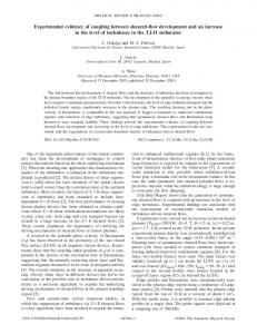
Finite-Difference Modeling of Noise Coupling between Power/Ground Planes in Multilayered Packages and Boards A. Ege Engin*, Krishna Bharath*, Madhavan Swaminathan*, Moises Cases+, Bhyrav Mutnury+, Nam Pham+, Daniel N de Araujo+ and Erdem Matoglu+ *Packaging Research Center, School of Electrical and Computer Engineering Georgia Institute of Technology, Atlanta GA, USA +IBM, xSeries eServer Development, 11400 Burnet Road, Austin, TX, USA Abstract Multilayered packages and boards, such as high performance server boards, contain thousands of signal lines, which have to be routed on and through several layers with power/ground planes in between. There can be noise coupling not only in the transversal direction through the power/ground planes in such a structure, but also vertically from one plane pair to another through the apertures and via holes. In addition, the continuous increase in power demand along with reduced Vdd values results in significant current requirement for the future chips. Hence, the parasitic effects of the power distribution system become increasingly more critical regarding the signal integrity and electromagnetic interference properties of cost-effective high-performance designs. We present a multilayer finite-difference method (M-FDM), which is capable of characterizing such noise coupling mechanisms. This method allows to consider realistic structures, which would be prohibitive to simulate using fullwave simulators. Introduction Increased power demand and reduced power supply voltage in integrated circuits (ICs) is leaving little or no room for error in high-speed signal integrity and power integrity analysis. According to International Roadmap for Semiconductors (ITRS), the power supply voltage (Vdd) that is 1.2V for 2005 is predicted to go below 1V in year 2012 [1]. The increased power demand along with reduced Vdd values result in significant current requirement for the future chips. Hence, the parasitic effects of the power distribution system become increasingly more critical. Power noise analysis for arbitrary shaped power layers and stack-ups becomes very important to achieve cost effective high-performance designs. High performance server boards contain thousands of signal lines, which have to be routed on and through several layers with power/ground planes in between as shown in Figure 1. Power/ground planes in electronic packaging and printed circuit boards (PCB) can be a major factor for noise coupling. There can be noise coupling not only in the transversal direction between two planes, but also vertically from one plane pair to another through the apertures and via holes. Excessive supply voltage fluctuations cause signal integrity problems. In addition, noise voltage that gets coupled to the edge of the board may cause significant electromagnetic interference. Hence, accurate modeling of power/ground planes is critical to estimate the noise levels. Power/ground planes in packages and PCBs generally have irregular geometries. There can be large apertures and splits in planes. Fields in different plane pairs can get coupled
1-4244-0152-6/06/$20.00 ©2006 IEEE
through these apertures. This can be regarded as a coupling by means of a wrap-around current on the edges of the planes. For narrow slots, a transmission-line based model has been proposed to take into account this interlayer coupling [2]. Electric and magnetic polarization currents have also been considered to compute coupling through electrically small cut-outs [3]. In this paper, a method to model arbitrary shaped non-overlapping plane structures is shown using the finitedifference method (FDM). To the best of the authors’ knowledge, there has been no efficient method available to analyze such structures with arbitrarily large holes in the planes. Hence, analysis of such structures has been only possible by using generic full-wave simulators, which are not capable of handling realistic structures due to their memory requirements and computational complexity.
Figure 1 Multilayered server board FDM has been recently applied as a simple and efficient method for the modeling of single plane pairs [4]. We extended FDM to multilayered planes in [5] by combining the admittance matrices of single plane pairs. In this paper, we present for the first time equivalent circuit models for such structures based on multilayer FDM. The resulting model reduces to the well-known bed-spring model for a single plane pair [5], [6]. For time domain analysis, the circuit model is readily available that can be included in a generic circuit solver such as Spice. A banded sparse matrix solver can be used for the solution of the network in frequency domain. Based on the proposed method, coupling between different layers through electrically large apertures can be modeled very accurately and efficiently. FDM for a single plane pair The underlying elliptic partial differential equation for the modeling of planes is a Helmholtz equation
1262 2006 Electronic Components and Technology Conference
(∇ T2 + k 2 )u = − jωµdJ z
(1)
where ∇ T is the transverse Laplace operator parallel to the 2
planar structures, u is the voltage, d is the distance between the planes, k is the wave number, and J z is the current density injected normally to the planes [7]. Problem definition is completed by assigning homogenous Neumann boundary conditions, which correspond to assuming a magnetic wall, or an open circuit, on the periphery of the planes. One method to solve the Helmholtz equation is by applying the finitedifference scheme. The 2-dimensional Laplace operator can be approximated as
∇ T2 u i , j = (u i , j −1 + u i , j +1 + u i −1, j + u i +1, j − 4u i , j ) / h 2 (2)
The cell-centered discretization scheme shown in Figure 2 results in a well-known equivalent circuit model. This can be shown by dividing both sides of (4) with − jωµd , resulting in:
(ui , j −1 + u i , j +1 + ui −1, j + ui +1, j − 4ui , j ) /(− jωµd )
length and u i , j is the voltage at node (i, j ) for the cell-
d
ui , j = h 2 J z
Cuc =
εh 2
(6)
d
and
Luc = µd
centered discretization as shown in Figure 2.
(7)
Substituting (6) and (7) in (5) yields:
ui,j+1
(u i , j −1 + u i , j +1 + u i −1, j + u i +1, j − 4 u i , j ) /(− jωLuc ) ui-1,j
ui,j
+ jωCuc u i , j = I z
ui+1,j
ui , j = ui+1, j
h h
Another way of representing this approximation, which is called the 5-point approximation, is through its stencil form:
1 1 = 2 1 − 4 1ui , j h 1
ui +1, j is outside of the plane boundary. Equations (8) and (9) can be represented using a unit cell as shown in Figure 3. This unit cell results in the well-known bedspring model for a plane consisting of inductors (Luc) between neighboring nodes, and capacitors (Cuc) from each node to ground.
(3)
R1
L1
Applying this 5-point approximation on the Helmholtz equation yields
ui , j −1 + ui , j +1 + u i −1, j + ui +1, j − 4ui , j + h k ui , j 2
= −h jωµdJ z 2
(4)
h
h
(a)
which gives a system of linear equations when applied to all nodes on the plane.
R1 R1
ε 2
(9)
where u i , j represents the voltage on a boundary cell and
Figure 2 Discretization of the Laplace operator
∇ ui , j
(8)
where I z is the total current injected into the cell. Homogeneous Neumann boundary conditions can be approximated as
ui,j-1
2 T
(5)
For a parallel-plate transmission line of equal length and width (h), the capacitance and inductance per unit cell can be obtained from the permittivity (ε), permeability (µ), and the distance between the planes (d) as:
2
with an error in the order of O( h ) , where h is the mesh
εh 2
+ jω
L1
L1 L1
C1
R1
G1
(b)
Figure 3 (a) Geometry and (b) electrical model of a unit cell for a single plane pair
1263 2006 Electronic Components and Technology Conference
Multilayer FDM The unit cell model shown in Figure 3(b) uses a common ground node. In a multilayered structure consisting of more than two planes, unit cells of different plane pairs can assign this ground potential to different planes. Therefore, such unit cells cannot be stacked on top of each other without any modification to model a multilayered plane. A straightforward stacking would short-circuit the elements between two ground connections, resulting in a completely wrong model. In order to obtain a model for the combined unit cell representing all the planes in the structure, consider the inductor elements in a unit cell as shown in Figure 4(a). L1 is the per unit cell (p.u.c.) inductance between plane 1 and plane 2, whereas L2 is the inductance between plane 2 and 3. Hence, reference planes are different in both models in Figure 4(b) and L2 would be short-circuited if the same nodes on plane 2 were connected with each other. In order to avoid that, the p.u.c. inductances can be combined as shown in Figure 4(c) using a mutual inductance and assigning plane 3 as the reference plane. This model can be extended in a similar way to any number of planes. Physically, this model is based on that there is a complete coupling of the magnetic field when the return current is on plane 3, as represented by the mutual inductance that is equal to L2.
R1
ε1
d1
ε2
d2
L1+L2 L1+L2
h
h
h d1
L2
L2
h2 L2 = µd 2 / 2, C 2 = ε 2 d2
R2
(b)
(a)
R1 L1+L2 L1+L2
L1+L2
R1
R1
C1
G1
L2 R2
L1+L2
R1
L1+L2
R1 L1+L2
C1
G1 L2
R1
L1+L2
L1+L2
C1
L2
L2
L2
R2
R1
C2
G2
G1 L2
L2 R2
L2
L2
Var
L2 L2
R1
R2
L1+L2 Plane 1
R2 R2
L2
L1+L2
L2
L2
L1+L2
L1+L2
R1
Val
R1
R1 L1+L2
L2
V1r
R1
L2
Plane 3
Ia
R2
G2
C2
L2
(a)
V1l
L2 L2
R2
L2
R1, R2, G1, G2 are the conductor and substrate losses at a given frequency
Plane 2
Plane 1
R2
L2
L2
L2
R1
G1
2
L1
L1
C1
L1+L2
L1 = µd1 / 2, C1 = ε 1
L1+L2 L2
L2
Plane 1
I1
R1
R2
L2 L2
R2
L2
R2
L2 L2
R2
Plane 2 Ib Vbl I2
L2
R2
L2
Plane 2
L2
Vbr
R2
G2 L2
C2
G2
Plane 2
Vbl
Vbr
(c)
Plane 3
Plane 3
(b)
(c)
Figure 4 (a) Side view of a unit cell for a 3 plane structure showing the current loops associated with the p.u.c. inductances. (b) P.u.c. inductance of each plane pair. (c) Combining the p.u.c. inductances by changing the reference planes In terms of the admittance parameters, this model can be derived using the indefinite admittance matrix. The model on top of Figure 4(b) can be represented as
I1 = Y1 (V1l − V1r ) where
C2
(10)
Figure 5 (a) Geometry and p.u.c. parameters. (b) Combined unit cell model for three planes. (c) Plane model consisting of multilayer unit cells
Y1 =
1 . jωL1
(11)
Since the reference nodes of the ports are different, the indefinite admittance matrix is required [8], which can be constructed as:
I1 Y1 − Y1 Val − Var = , − I1 − Y1 Y1 Vbl − Vbr
(12)
1264 2006 Electronic Components and Technology Conference
A B B A − B B B O O Y = B O O B A − B B B A
where V1l − V1r = (Val − Var ) − (Vbl − Vbr ) . Then the admittance of the bottom model in Figure 4(b) can be added as
− Y1 Val − Var I a I1 Y1 = = (13) I b I 2 − I1 − Y1 Y1 + Y2 Vbl − Vbr which corresponds to the admittance matrix of the model in Figure 4(c). The total unit cell can then be obtained as shown in Figure 5(b) for the example of three planes, where the bottom plane is chosen as the voltage reference plane. The p.u.c. parameters can be obtained from the permittivity ( ε i ), permeability ( µ ), loss tangent ( tan δ i ) and the thickness of each dielectric layer ( d i ) for the i-th plane pair as:
Li =
µd i h2 di
where A = −1 −1 − Z uc uc Y uc + 2−Z −1 −1 1 − Z uc − Z uc Y uc + 3Z uc −1 −1 − Z uc Y uc + 3Z uc O
−1
O
− Z uc
− Z uc
Y uc + 3Z uc
−1
−1
−1
− Z uc
and (14)
− Z −1 uc B= O −1 − Z uc
1 1 jω r µ + 2σt 2 σ Gi = ω r Ci tan δ i Ri =
where h is the mesh length, and a constant conductivity ( σ ) and thickness (t) is assumed for each conductor. The p.u.c. resistance (Ri) and conductance (Gi) can be obtained at a given angular frequency ω r , where a significant portion of the considered signals are concentrated in the spectrum. Construction of the Multilayer FDM Matrix An equivalent circuit model such as shown in Figure 5, based on the T-unit cells can be solved using a common circuit solver. However, direct solution of the FDM equation using a linear equation solver can improve the memory requirements and speed, since the resulting admittance matrix is a sparse banded matrix. Based on the plane model in Figure 5, a linear equation system can be obtained which can be written in matrix form as:
YU = I
O
−1 − Z uc −1 Y uc + 2 Z uc
(17)
2
Ci = ε i
(16)
A and B are (kM × kM ) matrices for (k+1) planes, assuming that the nodes are numbered starting from the top node in the lowest row, increasing in the vertical direction to the bottom node, then starting with the next cell in the x direction until the last cell, and then starting with the next row. Hence, Y is a (kMN ) × (kMN ) matrix. The unit-cell −1
matrices Y uc and Z uc can be obtained similar to (13) as
Y uc
(15)
where U and I are the cell voltage and current vectors. The admittance matrix Y for solid multilayered rectangular planes, discretized with M cells in x -direction and with N cells in y -direction, can be written as:
(18)
− Y1 Y1 − Y1 Y1 + Y2 − Y2 =
− Y2 O O
O − Yk − 2
− Yk − 2 Yk − 2 + Yk −1 − Yk −1
− Yk −1 Yk −1 + Yk (19)
and
1265 2006 Electronic Components and Technology Conference
−1
Z uc
1 Z1 −1 Z 1 =
−1 Z1
1 1 + Z1 Z 2 −1 Z2
−1 Z2 O
O
O −1 Z k −2
1
−1 Z k −2
1 + Z k −2 Z k −1 −1 Z k −1
−1 Z k −1 1 1 + Z k −1 Z k (20)
where Yi and Z i can be obtained similar to (14) and unit cell
6. Only port 2 is excited, which is between the middle and bottom planes. The large amount of current on the top plane indicates coupling of the plane pairs through wrap-around currents. (0,22.9)mm Port 1
(45.7,22.9)mm Plane 1
Plane 3
Plane 1 45.7mm
parameters of a single plane pair [6] as
Plane 2 (30.5,30.5)mm
Plane 3
(15.2,15.2)mm 45.7mm
Yi = jωCi + ωCi tan δ i
2 jωµ Z i = 2 jωLi + + 2 σt σ
(21)
The admittance matrix Y is a sparse banded matrix. This becomes important for storage of the matrix elements and the solution of the matrix equation. In practical applications, the planes can have non-rectangular boundaries or they can even contain holes. In this case, wherever a plane is missing in a −1
unit cell structure, the p.u.c. matrix Z uc , which represents the connections from this unit cell to the neighboring unit cells, is modified. In this way, practical structures can also be considered very efficiently. To illustrate this, if the middle −1
plane in a three plane structure is missing in a unit cell, Z uc can be modified as 1 −1 Z uc = Z 1 + 2 jωL2 0
Port 2
Plane 2
0 0
Figure 6 Three-plane structure with a hole in the middle plane The multiple plane structure in Figure 6 was fabricated using FR4 dielectric layers with εr=4, tan δ = 0.02, and thicknesses of 5mils for each layer. Figure 8 shows that there is an excellent agreement regarding the transmission coefficient S12 obtained from the measurement and the proposed method. S12 is solely due to the coupling through the aperture, and could be very accurately captured. This is a large amount of coupling, which could cause a signal integrity problem if, for example, top and bottom planes were assigned to different voltage levels. The same structure was also simulated using a full-wave simulator, Sonnet, giving similar results. All the simulations were done on an Intel Xeon workstation with a 3GHz CPU and 3.25GB RAM. Calculation of each frequency point required 1.35s using FDM implemented in Matlab, and 94s using Sonnet, resulting in a speed-up of 70X.
(22)
which can be obtained by simply removing the inductance associated with plane 2 in Figure 4(c). The factor of 2 before the inductance is necessary, if the inductance is defined according to (14). Numerical Results Consider the three-plane structure in Figure 6 with a hole in the middle plane (plane 2). Port 1 is defined between plane 1 and 2; and port 2 is between plane 2 and plane 3. In such a three-plane structure, there will be three plane pairs. These plane pairs are coupled at their boundaries. Current flowing into the boundary of a plane pair will spread into other plane pairs, which results in a wrap-around current. Figure 7 shows the magnitude of current at 1.5GHz, which was simulated using Sonnet, for the structure in Figure
Figure 7 Simulated wrap-around current
1266 2006 Electronic Components and Technology Conference
A high level of vertical noise coupling was observed through an aperture in the middle plane for the test structure. The proposed method could accurately predict this noise coupling, which can cause signal integrity (SI) and electromagnetic interference (EMI) problems. The multilayered finite difference method is based on unit cells. Hence we believe that it will be very useful to model the SI and EMI behavior of realistic structures with multilayered planes having arbitrary shapes.
-10
mag(S12) [dB]
-20 -30 -40
Multilayer FDM Sonnet Measurements
-50
References 1. 2004 International Roadmap for Semiconductors (ITRS) [http://public.itrs.net] 2. R. Ito and R.W. Jackson, “Parallel plate slot coupler modeling using two dimensional frequency domain transmission line matrix method,” in Proc. IEEE EPEP, pp. 41–44, 2004. 3. J. Lee, M.D. Rotaru, M.K. Iyer, H. Kim, and J. Kim, “Analysis and suppression of SSN noise coupling between power/ground plane cavities through cutouts in multilayer packages and PCBs,” IEEE Trans. Adv. Packag., vol. 28, no. 2, pp 298–309, May 2005. 4. O. M. Ramahi, V. Subramanian, and B. Archambeault, “Simple and efficient finite-difference frequency-domain algorithm for study and analysis of power plane resonance and simultaneous switching noise in printed circuit boards and chip packages,” IEEE Trans. Adv. Packag., vol. 26, pp. 191–198, May 2003. 5. A. E. Engin, M. Swaminathan, Y. Toyota, “Finite Difference Modeling of Multiple Planes in Packages,” Proc. 17th International Zurich Symposium on Electromagnetic Compatibility, Singapore, Mar. 2006. 6. J. Kim and M. Swaminathan, “Modeling of multilayered power distribution planes using transmission matrix method,” IEEE Trans. Adv. Packag., vol. 25, no. 2, pp. 189-199, May 2002. 7. T. Itoh, Ed., “Numerical Techniques for Microwave and Millimeter-Wave Passive Structures,” John Wiley & Sons, 1989. 8. Janusz A. Dobrowolski, “Introduction to Computer Methods for Microwave Circuit Analysis and Design,” Artech House, 1991.
-60 -70 0
1
2 3 4 Frequency [Hz]
5
6 9
x 10
(a)
Multilayer FDM Sonnet Measurements
phase(S12) [degrees]
200
100
0
-100
-200 0
2 4 Frequency [Hz]
6 9
x 10
(b) Figure 8 (a) Transmission coefficient magnitude and (b) transmission coefficient phase for the structure in Figure 6 Conclusions This paper presented a new method to model multiple plane pairs coupled through apertures. It is based on an extension of the finite difference method to multiple plane pairs. An equivalent circuit model was also presented. Based on this method, the wrap-around current around the apertures can be taken into account very accurately. There was an excellent agreement between the proposed method and measurements for a multilayered structure with three planes. A speed-up of 70X was observed compared to the run time of a full-wave simulator for this structure.
1267 2006 Electronic Components and Technology Conference