Firm-core Virtual FPGA for Just-in-Time FPGA Compilation Roman Lysecky, Kris Miller, Frank Vahid
Kees Vissers
University of California, Riverside {rlysecky, kmiller, vahid}@cs.ucr.edu
Xilinx Corp.
[email protected]
Abstract Just-in-time (JIT) compilation has been used in many applications to enable standard software binaries to execute on different underlying processor architectures, yielding software portability benefits. Researchers previously introduced the concept of a standard hardware binary to achieve similar portability benefits for hardware, using a JIT compiler to compile the hardware binary to an FPGA. The JIT compiler includes lean versions of technology mapping, placement, and routing algorithms that implement the standard hardware binary on a simple custom FPGA fabric designed specifically for JIT compilation. While developing a custom FPGA may be feasible for some applications, we propose implementing the simple FPGA fabric as a virtual FPGA. In this paper, we present a virtual FPGA, described using structural VHDL and thus representing a firm core that a designer can synthesize onto an existing FPGA. We synthesized the firm-core virtual FPGA onto Xilinx Spartan physical FPGAs and then mapped 18 benchmark circuits onto the virtual FPGA. Our results show a 6X decrease in performance and 100x more hardware resource usage, for the virtual FPGA approach compared to mapping the circuits directly to the physical FPGA fabric. While the hardware overhead is large, large commercial FPGA capacities may still mean that some applications can utilize a virtual FPGA approach if portability is more important than resource utilization. Furthermore, our work provides a baseline for future virtual FPGA approaches that may reduce the performance or area overhead through various means.
Keywords Virtual FPGA, FPGA, configurable logic fabric, just-in-time compilation, hardware/software partitioning, platforms, systemon-a-chip, dynamic optimization, self-improving chips, warp processors.
1. Introduction Just-in-time (JIT) compilation for Field-Programmable Gate Arrays (FPGAs) enables the development of a standard hardware binary, as well as new technologies such as warp processing [13]. Standard hardware binaries would provide portability, allowing designers to use a single hardware netlist to configure a multitude of different FPGAs with different underlying architectures. An FPGA supporting JIT compilation would be capable of transparently mapping the standard hardware binary to the FPGA’s configurable logic while optimizing the hardware design for that particular FPGA. In software design, just-in-time compilation provides powerful benefits. Just-in-time compilation involves downloading a software binary format onto a chip, and then dynamically and transparently re-compiling that binary to the instruction set of the particular processor on that chip. The main benefit is that of binary portability – standard tools can be used to create a binary, and that same binary can be downloaded onto many different platforms. Modern x86 processors, including Intel’s Pentium and
Transmeta’s Crusoe and Effecion processors, incorporate JIT compilation, wherein x86 binaries are dynamically translated to and optimized for the chip’s underlying RISC or VLIW instruction set [8][17]. As FPGAs continue to find their way into more end-products, such as TV set-top boxes, cell phones, medical equipment, etc., the concept of a “binary” changes from that of just a microprocessor program, to a more general concept of a platform binary providing the configuration bits for a chip, possibly providing the configuration for an FPGA, a software program, or both. Ideally, a designer could create a standard binary for an FPGA and then map that standard binary to any of multiple FPGA architectures. Unfortunately, there presently does not exist the concept of a standard hardware binary for FPGAs. Netlist formats are specific to a particular FPGA architecture, and FPGA architectures vary significantly. Consider the example of a TV set-top box. Cable TV companies may transparently upgrade software within such boxes by downloading new software binaries. This works even though newer boxes may contain more advanced versions of the microprocessor, since newer processors often support older binaries or the binary can be JIT compiled to the different processor. Yet, such boxes increasingly rely on FPGAs for video processing, and so ideally as part of the platform binary we could download new hardware binaries for the FPGAs as well, either to add new features or to fix bugs. However, newer boxes may contain newer or different FPGA architectures, complicating upgrades. By incorporating a JIT compiler within the FPGAs, a standard hardware binary could be transmitted and JIT compiled to the different FPGAs. JIT compilation for FPGAs is also useful, in fact essential, for warp processors that perform dynamic hardware/software partitioning [13]. Warp processors dynamically optimize an executing software binary by moving software kernels to on-chip configurable logic, resulting in better performance and lower energy consumption. At the heart of warp processors, a JIT compiler is required to implement the synthesized hardware circuits onto the on-chip configurable logic fabric. Another potential application of JIT FPGA compilation could be future desktop, laptop, and handheld computers that allow users to add FPGA to their computing systems to improve performance. In a similar manner to how today’s computer users expanding the available memory by adding RAM, users could simply plug-in additional FPGA resources or perhaps plug-in a faster FPGA device with more extensive hardware resources. Assuming a standard hardware binary, the operating system could re-implement the hardware binary or platform binary to utilize the newly added FPGA. An example application benefiting from additional FPGA resources might be fingerprint or speech recognition, for which adding FPGA might improve speed from minutes down to seconds. Previously, researchers developed a lean set of JIT FPGA compilations tools that compiles a standard hardware netlist onto
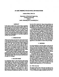
Figure 1: (a) Simple FPGA configurable logic fabric (b) configurable logic block (CLB), and (c) switch matrix (SM) architecture. a b c SM
SM
CLB
d e f
SM
Adj.
CLB
LUT
LUT
CLB SM
0 1 2 3 0L 1L2L 3L
SM
SM
o1
o2
o3
Adj. CLB
3L 2L 1L 0L 3 2 1 0
3L 2L 1L 0L 3 2 1 0
o4
0 1 2 3 0L 1L 2L 3L
Configurable Logic Fabric (a)
Configurable Logic Block (b)
a simple custom configurable logic fabric [10][11]. Compiling to an FPGA is notoriously time-consuming, however, due in large part to placement and routing. Yet, a JIT FPGA compiler must execute on-chip on lean processing resources, perhaps just a small 32-bit embedded processor with limited memory, with that processor even perhaps a soft processor core on the FPGA itself. Thus, instead of targeting a commercially available FPGA, those researchers developed a simple FPGA fabric specifically designed for fast place and route, in conjunction with their JIT compilation tools, in order to enable the development of their lean tools that execute using very limited memory resources and execution time while producing good results. We could further increase the usefulness of JIT FPGA compilation if we could extend the JIT compilation approach to support use of any existing FPGA or future FPGA products. However, a set of JIT compilation tools supporting such a broad range of FPGAs would require much more memory resources and longer execution, resulting in a set of tools no longer suitable for lean on-chip execution. Alternatively, one could implement the simple custom configurable logic fabric by mapping the fabric to an existing FPGA, as the simple fabric is actually just another circuit, meaning the simple fabric would be a “virtual FPGA.” By providing a layer of abstraction between the configurable logic fabric targeted by the JIT FPGA compiler and the underlying FPGA device, we can create an FPGA supporting JIT compilation using any FPGA. However, a virtual FPGA has several drawbacks. By adding a layer of abstraction, the virtual FPGA will require some amount of additional hardware resources to implement the components within configurable logic fabric. Therefore, a virtual FPGA will have a reduced amount of usable configurable logic compared to the underlying physical FPGA. Additionally, a hardware circuit implemented using a virtual FPGA would have a longer critical path due to the additional hardware resources through with a signal must travel. Previously, other researchers have also investigated implementing virtual FPGAs. Both Torresen [14][15][16] and Sekanina [12] proposed developing similar virtual configurable logic fabrics consisting of coarse-grained functional units. The functional units could be programmed to perform a few different logic operations as well as provide the routing mechanism with their fabric. Furthermore, both efforts also focused on enabling their virtual FPGAs to support storing multiple bitstreams. During execution, the virtual fabric provided the ability to quickly select
Switch Matrix (SM) (c)
a new bitstream and re-program reprogram the configurable logic to one of several pre-determined configurations. Lagadec et al [9] proposed a system in which a user defines a virtual FPGA fabric using a high level description. In this methodology, the high-level abstraction would be used to automatically create the virtual fabric and placement and routing tools required to target the new fabric. While the proposed system could support any level of granularity within the FPGA, their work focused a coarse-grained capable of performed addition, subtraction, maximum, or minimum comparisons on two 8-bit inputs. Fornaciari [7] also proposed a virtual FPGA system. However, a virtual FPGA in this work refers to a methodology for swapping in FPGA configurations on a physical FPGA devices using operating system support, much like virtual memory systems. In this paper, we present a virtual FPGA fabric, based on the configurable logic fabric from [10]. The main difference from previous virtual FPGA work is that our fabric is a fine-grained fabric, much like existing commercial FPGAs. To ensure we can implement the virtual fabric using any available FPGA, we developed the virtual fabric as a synthesizable VHDL model an implemented the virtual fabric using a low cost FPGA. Using our virtual FPGA, one can develop an FPGA supporting a standard hardware binary as well as develop a warp processing system that relies on JIT compilation for dynamically re-implementing critical software kernel in hardware. In this paper, we describe a simple configurable logic fabric, our VHDL model, and experiments that evaluate the performance and power overhead of our virtual FPGA approach.
2. Just-in-Time FPGA Compilation JIT compiler for FPGAs consists of lean versions of technology mapping, placement, and routing algorithms. Starting with the standard hardware binary, a JIT compiler performs technology mapping to map the hardware onto to the LUTs within the configurable logic and further packs the LUTs into CLBs. Once mapped, the JIT compiler determines the location of each CLB within the configurable logic using our greedy placement algorithm. The placement algorithm attempts to assign location to the CLBs to reduce the critical path of the circuit while ensuring the circuit can be routed. Finally, the JIT compiler performs routing during which the actual wire segments used to connect CLBs together are determined. Implementing the required lean CAD tools for on-chip execution is not trivial. Existing FPGA CAD tools are capable of
Figure 2: Virtual configurable logic block consisting of four 3-input LUTs (two 3-input 2-output LUTs. def abc Adj. CLB
pdout pdin
Adj. CLB
o1
o2
producing highly optimized hardware circuits. However, these tools suffer from very large data memory usage, often exceeding 100 megabytes, and long execution, ranging anywhere from minutes to hours. Therefore, the researchers in [11] designed a JIT compiler by focusing on developing lean algorithms that use as little data memory as possible and have fast execution times. These design goals will inherently restrict the ability of the JIT compiler to produce designs as highly optimized as their desktop counterparts will. However, their on-chip CAD tools still produce hardware circuits of acceptable quality. Furthermore, researchers have also developed a simple FPGA fabric specifically designed to enable the development of a lean JIT compiler for FPGA [10]. Figure 1(a) presents their custom configurable logic fabric. The FPGA consists of an array of configurable logic blocks (CLBs) surrounded by switch matrices (SM) for routing between CLBs. Each CLB is connected to a single switch matrix to which all inputs and outputs of the CLB can be connected. The switch matrices handle routing between CLBs and can route signals in one of four directions to an adjacent SM or to a SM two rows apart vertically or two columns apart horizontally. Figure 1(b) shows our configurable logic block architecture. Each CLB consists of two 3-input 2-output LUTs and four flip-flops optionally connected to each of the four outputs. The CLBs further support carry chains by providing direct connections to adjacent CLBs as well as connections between the LUTs within the CLB. Finally, Figure 1(c) shows the switch matrix architecture. Each switch matrix is connected using short channels for routing between adjacent switch matrices and long channels for routing between every other switch matrix. Routing through the switch matrix can only connect a wire from one side with a given channel to another wire on the same channel but a different side of the switch matrix. Additionally, each short channel is paired with a long channel and can be connected together within the switch matrix (indicated as a circle where two channels intersect) allowing nets to be routed using short and long connections.
3. Virtual FPGA In developing a virtual FPGA, we identified two possible methods for implementing the virtual FPGA: • Firm-core virtual FPGA: A structural VHDL model of the target FPGA fabric that can be synthesized onto any physical FPGA device using any suitable synthesis tools. • Hard-core virtual FPGA: A customized implementation consisting of a partial bitstream for a specific FPGA device, in which the un-programmed bits within the
o3
o4
bitstream are used to store the configuration for the virtual fabric. We used the terms firm-core and soft-core from general descriptions of IP (Intellectual Property) cores that distinguish between soft, firm, and hard IP cores (e.g., Virtual Socket Interface Alliance [18]). The firm-core virtual FPGA provides many advantages over the hard-core approach. Not only can the VHDL model be synthesized for any number of FPGAs devices, but a designer can also use the VHDL model for simulation. Furthermore, one can quickly add new features and incorporate architectural changes into the virtual fabric without requiring any time consuming modifications that would be required in a hard-core virtual FPGA. Alternatively, in the hard-core virtual FPGA, one can implement the virtual fabric by exploiting specific FPGA’s underlying physical components and re-using the physical routing resources and configurable components. In this approach, the bitstream used to configure the physical FPGA would consist of two intertwined elements: a fixed partial configuration creating the virtual FPGA and a variable configuration used to program the behavior of the virtual fabric. While this approach is not portable across different FPGA devices (or even different devices within the same family of FPGAs), a hard-core virtual FPGA would require less overhead and provide better performance than the firm-core approach. In [4], researchers developed a large dynamically programmable crossbar switch using an FPGA. The researchers efficiently implemented the programmable crossbar switch by exploiting the physical architectural features to implement the switch fabric. While the hard-core virtual FPGA has many advantages, our initial goal in developing a virtual fabric is to provide a very flexible and portable virtual FPGA. Therefore, the work in this paper focuses on the firm-core virtual FPGA design.
3.1 Combination Logic Blocks The configurable logic block presented in Figure 1 consists of two 3-input 2-ouptut LUTs, four flip-flops, and logic use to provide support for carry chains and enabling or bypassing the flip-flops. Furthermore, in a typical FPGA, the CLB would also contain SRAM bits for storing the CLBs configuration, including the contents of the LUTs. Figure 2 presents our virtual implementation of the configurable logic block. We represent each of the 3-input 2-output lookup tables as a two 3-input 1output lookups with same 3-inputs. The individual lookup tables are implemented using an 8-bit shift register whose outputs connect to an 8-to-1 multiplexor that produces the single bit
Figure 3: Virtual tri-state buffer based switch matrix: (a) overall switch matrix architecture, (b) internal routing switch, and (c) configurable logic block (CLB) interface. 0
1
0L
1L
Internal Switch a b c d e f o1 o2 o3 o4
0L 1L
IS
IS
IS
IS
IS
1
0L 1L
IS
1 CLB
Interface 0
IS
IS
0
SM Input SM Output 0
1
0L
1L
From/To CLB
Switch Matrix (Tri-state Buffer) (a)
Internal Switch (b)
output. The virtual CLB connects the LUT’s output from the multiplexor to the CLB’s sequential elements implemented using flip-flops. The flip-flop outputs and the LUT’s output are connected to a 2-to-1 multiplexor that allows the configuration to select the combinational of sequential output. Furthermore, the least significant input to the LUTs can come from either the CLB’s main inputs c or f, or from the adjacent CLB’s and LUT’s outputs. We implemented this programmability using two 2-to-1 multiplexors for each of the LUTs. One can program the virtual CLB by shifting in a bitstream using in on the pdin input that connects to the shift register used to the store the CLB’s configuration. A typical FPGA would store the bitstream using an SRAM-based shift register. However, our virtual FPGA implements the shift register using sequentially connected flip-flops. Figure 2 presents the configuration shift registers and demonstrates how the various configurable bits are connected with the virtual CLB. The output from the last flip-flop of the configuration shift register, pdout, will be connected to the other CLBs and switch matrices throughout virtual FPGA to create the entire configuration shift register interface for programming the fabric.
3.2 Switch Matrix In a traditional FPGA, the switch matrices providing routing resources through programmable interconnects. The programmable interconnects can be implemented as a single pass transistor connecting two wires. Furthermore, with this implementation, the wires connected within the switch matrix can act as either inputs or outputs. However, while VHDL does provide bi-directional ports and signals, developing a virtual switch matrix using bi-directional signals would be difficult, if not possible impossible, as we need to know beforehand what elements of the circuit will be driving the inputs and receiving the outputs. Instead, we implemented the virtual switch matrices by replacing each wire connected to a switch matrix with a pair of wires with one input and one output. We implemented the switch matrices by trying two different approaches. Our first approach is a tri-state buffer based switch matrix (TSM). We designed the virtual TSM to closely replicate the behavior of the original switch matrix. However, because or virtual switch matrices have individual input and outputs, we require twice as many configurations bits in the bitstream to
CLB Interface (c)
program the switch matrix. The second virtual implementation is a multiplexor-based switch matrix (MSM). The virtual MSM does not replicate the exacting routing behavior of the original SM but instead provides the same routing functionality using multiplexors. We describe the two virtual switch matrix implementations next.
3.2.1 Tri-state Buffer Based SM Figure 3 presents our virtual tri-state buffer based switch matrix (TSM). While the actual switch matrix supports four short channels and four long channels, the virtual TSM presented in Figure 3(a) shows a smaller version of the switch matrix with only two short channels and two long channels for illustration purposes. The TSM has three different internal routing elements. First, the TSM contains an internal switch (IS) that connects the wires on the same channel from different sides of the switch matrix. Additionally, the TSM uses another internal switch to connect the long and short channels within the switch matrix, depicted as the circular IS component. Finally, the CLB interface is used to connect the switch matrix’s inputs and outputs to the CLB associated with that SM. Because SM can connect the CLB’s inputs and outputs to any of the inputs or outputs of the SM, we include a CLB interface for each routing channel within the SM. Figure 3(a) presents the details on how we implement the TSM’s internal switches (IS). The same IS design is used for routing signals on the same channel and routing between the long and short channels. Internally, the IS consists of 12 tri-state buffers. We configure each tri-state buffer using an individual flip-flop from the configuration shift register to program the internal switch. Each tri-state buffer routes an incoming channel wire to an output wire on different sides of the internal switch. Figure 3(b) presents the CLB interface for connecting the inputs and outputs of the CLB to all of the TSM’s routing channels. The interface consists of ten tri-state buffers. The interface connects the CLB’s input signals using six of the tristate buffers to the incoming SM routing channel, SM Input. The CLB interface also connects the CLB’s outputs to the outgoing SM routing channel, SM Output, using the remaining four tri-state buffers.
Figure 4: Virtual multiplexor-based switch matrix: (a) overall switch matrix architecture highlighting internal mutliplexor connections and (b) configurable logic block (CLB) interface 0
1
0L
1L
a 0L
0L
1L
1L
1
1
0
0
CLB Interface
4
0
1
0L
1L
North
0 1 0L 1L
East
Switch Matrix (Mux) (a)
3.2.2 Multiplexor Based SM Figure 4 presents our virtual multiplexor-based switch matrix (MSM). The SM presented in Figure 1 allows a wire to be routed on a given channel from one side of the SM to the same channel on another side of the SM. Additionally, the original SM can route a wire from a short channel to the associated long channel. While the MSM does not present and exact implementation of the SM, the virtual MSM will provide the same functionality. We also note that the programming bits for this SM would be different from the virtual TSM implementation, however, translating between the two bitstream formats is a straightforward task. The MSM consists of two different programmable interfaces. For each output channel of the switch matrix, the MSM uses a 12-to-1 multiplexor to select which input routing channel or CLB output is connected to that output. For a given channel, the possible connections include input signal of the same channel from different sides of the SM, the long or short routing channels associated with that output channel, or any of the four output signals from the CLB. Figure 4(b) presents the CLB interface used within the MSM to connect the CLB’s inputs and output to the SM’s routing channels. In this virtual SM implementation, only a single CLB interface is required. The CLB interface uses four 32-to-1 multiplexors to connect the routing channels of the SM to the CLB’s inputs. Each multiplexor can select which of the 32 incoming short or long channels is connected to a given CLB input. Finally, the interface simply passes through the CLB’s output directly to the output of the CLB interface.
4. Experiments We evaluated our firm-core virtual FPGA implementation both in terms of the resource overhead of the virtual fabric as well as the performance overhead. We implemented our virtual FPGA by synthesizing both VHDL models for a Xilinx Spartan-IIE FPGA using Xilinx ISE 6.2 synthesis tools [19]. The Spartan-II devices are low cost FPGAs that one can easily incorporated into a JIT FPGA compilation framework. Table 1 presents the resulting amounts of resources within the Spartan FPGA required to implement a virtual CLB and virtual switch matrices. The virtual CLB requires 22 LUTs to implement the various multiplexors used for accessing the LUTs and
d
4
0 1 0L 1L
From/To CLB
c
b
f
e
4
o1 o2 o3 o4
4
0 1 0L 1L
0 1 0L 1L
South
West
o1 o2 o3 o4
CLB Interface (b) providing routing within the CLB. Considering the CLB design consists of 4 LUTs, the virtual CLB requires roughly 5X more LUT resources. However, the implementation of the configuration shift register using flip-flops presents and even larger overhead. Overall, the virtual CLB requires 42 flip-flops, 32 of which are used to implement the configuration shift register. Compared to the original CLB design that consists of four flip-flops, the virtual CLB requires 10X more flip-flops. The tri-state buffer based SM and the multiplexor-based SM provide an interesting tradeoff between the number of LUTs and flip-flops require for both implementations. While the TSM requires 64 LUTs to the implement the virtual SM, the MSM requires over 5X times more. On the hand, the MSM requires 158 flip-flops to implement the configuration register, whereas the TSM requires 4X more flip-flops because the TSM requires more configuration bits. Considering that the each CLB is directly connected to a SM, the basic element within our virtual FPGA is the combination of a SM and CLB. Table 1 presents the total resources used for each SM and CLB combination. A CLB connected to a TSM requires a total of 86 LUTs and 554 flipflops, or 21X times more LUTs and over 100X times more flipflops than the original FPGA. A CLB connected to a MSM requires a total of 354 LUTs and 200 flip-flops, or 88X times more LUTs and 50X more flip-flops. Depending on the organization and hardware resources of the physical FPGA the virtual fabric is implemented on, a designer can choose between the two different implementations to maximize the virtual FPGA Table 1: Physical FPGA resources required for virtual FPGA components. Virtual FPGA CLB TSM MSM CLB+TSM CLB+MSM
Physical FPGA Resources LUTs 22 64 332 86 354
Total FFs 42 512 158 554 200
Config. FFs 38 508 196 546 234
Figure 5: Critical path (ns) for a custom FPGA, our firm-core virtual FPGA with tri-state buffer SM, and our firm-core virtual FPGA with multiplexor-based SM for several MCNC benchmark circuits.
Critical Path (ns)
2000 Custom FPGA
Virtual FPGA (TSM)
Virtual FPGA (MSM)
1500 1000 500
g ra ge : Av e
ts en
se q
4 s3 17 85 84 .1
8
23
s2 9
s3 8
Benchmark Circuit
s1 4
ex 3
sc
m is
fri
p ex 5
t ic el lip
e6 4
p ds i
eq di ff
de s
y ke
x4
bi g
ap e
ap e
al u
4
x2
0
Figure 6: Performance overhead of our firm-core virtual FPGA with tri-state buffer SM and our firm-core virtual FPGA with multiplexorbased SM compared to a custom FPGA fabric for several MCNC benchmark circuits. 12 Virtual FPGA (TSM)
Performance Overhead
10
Virtual FPGA (MSM)
8 6 4 2
size that can fit within the physical FPGA. While the large amount of resources overhead for implementing the virtual FPGA is expected, we are currently working to reduce this large size overhead. However, while the virtual FPGA requires up to 100X more hardware resources, a designer could use a large 2 million gate FPGA to implement a virtual FPGA with 20,000 logic gates, providing about the same amount configurable logic as FPGAs produced in the mid 1990s. Although the firm-core virtual FPGA provides much less configurable logic than the underlying physical FPGA, our virtual FPGA will be useful for some applications in which the portability of a hardware binary is far more important than the total FPGA size. Another important aspect of our firm-core virtual FPGA is the resulting performance overhead. We analyzed the delay through the various virtual FPGA components by synthesizing and downloading the bitstreams for our virtual FPGA implementations to a Spartan-IIE FPGA using the Digilent Digilab 2SB FPGA system board [6]. Using several different configurations, we determined the delays through the various elements of the virtual fabric. Using this data, we estimated the performance overhead of our virtual FPGA fabric for several MCNC benchmark circuits [20] against a custom implementation of the original FPGA
ts en g Av er ag e:
Benchmark Circuit
se q
fri sc m is ex 3 s1 42 3 s2 98 s3 84 s3 17 85 84 .1
5p ex
tic lip el
4 e6
ds ip
q di
ffe
s de
4
ey gk bi
2
ex ap
ex ap
al
u4
0
shown in Figure 1 implemented using the UMC 0.18 µm technology process. Starting with the BLIF specification for the benchmarks circuits, we first mapped each circuit to 3-input 1-ouput LUTs using FlowMap [5]. We then packed the LUTs together into the 3input 2-output LUTs and further into CLBs using VPR’s T-VPack [1][3]. We then determined the placement for each circuit using the VPR’s bounding box placement algorithm [1][2]. Finally, we routed the benchmark circuits using VPR’s timing-driven router using the ROCR routing algorithm provided by researchers in [11]. Figure 5 presents the critical path in nanoseconds for 18 MCNC benchmark circuits implemented on a custom FPGA, our virtual FPGA using the TSM, and our virtual FPGA using the MSM. Similarly, Figure 6 presents the performance overhead of both firm-core virtual FPGA implementations compared to the custom FPGA. On average, the virtual fabric with tri-state buffer based SMs resulted in a 6.4X performance overhead. On the other hand, while the multiplexor-based switch matrix requires more LUTs than the TSM, the delay though the MSM only resulted in a slightly slower circuit. On average, the virtual fabric incorporating a MSM resulted in a 6.8X performance overhead. Although the virtual FPGA implementations have a large
resources overhead, the decrease in performance of our virtual FPGA is not as significant. However, as mentioned, a hard-core virtual FPGA developed by exploiting the underlying physical components of a FPGA would result in a greatly reduced performance overhead, and we are currently working on this effort.
5. Conclusions and Future Work We presented an initial implementation of a firm-core virtual FPGA fabric that we can use to create a FPGA supporting Just-inTime FPGA compilation, and thus a standard hardware binary, using any existing FPGA. We implemented the firm-core virtual FPGA using a VHDL model of a simple FPGA fabric previously designed to support JIT FPGA compilation. In designing the virtual FPGA, we presented two different switch matrix architectures that provide a tradeoff between which hardware resources, LUTs or flip-flops, are required when synthesizing the virtual fabric. The virtual FPGA requires 100X more hardware resources to implement and results in a 6X performance overhead. However, even with this hardware overhead, the large capacity of current commercially available FPGAs enables a designer to create a virtual FPGA with tens of thousands of configurable gates. Such a virtual fabric can be useful for many applications, especially those applications in which hardware portability is essential. Our work can be considered as a “baseline” upon which future work on firm-core virtual FPGAs might improve. We are currently investigating improvements to our virtual FPGA fabric to reduce the area overhead. Furthermore, we are also investigating a hard-core virtual FPGA fabric. By targeting a specific FPGA device and exploiting the physical LUTs and routing resources, the hard-core virtual FPGA will require much fewer hardware resources and result in a lower performance overhead. However, a hard-core virtual FPGA will not be portable to other FPGA devices, even within the same family of FPGAs. Hence, we are also investigating the possibility of developing a generalized approached to creating a hard-core virtual FPGA that would allow the hard-core fabric to ported to other devices within the same FPGA family. Our future work is also focused on how we can better synthesize our firm-core virtual FPGA by synthesizing our VHDL model to different FPGA devices. Some FPGA devices allow the LUTs within the FPGA to be configured as a shift register that we can use to directly store our configuration bits instead of using flip-flops. However, ensuring that the synthesis tools recognize that our configuration bits can be implementing using the shift register functionality may require some modifications to our firm-core virtual FPGA model.
6. References [1] Betz, V., J. Rose, A. Marquardt. Architecture and CAD for Deep-Submicron FPGAs. Kluwer Academic Publishers, 1999.
[2] Betz, V., J. Rose. VPR: A New Packing, Placement, and Routing for FPGA Research. International Workshop on Field Programmable Logic and Applications (FPLA), 1997. [3] Betz, V., J. Rose, A. Marquardt. VPR and T-VPack: Versatile Packing, Placement and Routing for FPGAs. http:// www.eecg.toronto.edu/~vaughn/vpr/vpr.html, 2003. [4] Blodget, B., S. McMillan, P. Lysaght. A Lightweight Approach for Embedded Reconfiguration of FPGAs. Design Automation and Test in Europe Conference, 2003. [5] Cong, J., Y. Ding. FlowMap: An Optimal Technology Mapping Algorithm for Delay Optimization in Lookup-Table based FPGA Designs. IEEE Trans. On Computer-Aided Design of Integrated Circuits and Systems, Vol. 13, No. 1, pp. 1-12, 1994. [6] Digilent, Inc., http://www.digilentinc.com, 2004. [7] Fornaciari, W., V. Piuri. Virtual FPGAs: Some Steps behind the Physical Barrier. Workshop on Parallel and Distributed Processing (IPPS/SPDP), 1998. [8] Klaiber, A. The Technology Behind Crusoe Processors. Transmeta Corporation White Paper, 2000. [9] Lagadec, L., D. Lavenier, E. Fabiani, B. Pottier. Placing, Routing, and Editing Virtual FPGAs. International Conference on Field Programmable Logic and Applications (FPL), 2001. [10] Lysecky, R., F. Vahid. A Configurable Logic Architecture for Dynamic Hardware/Software Partitioning. Design Automation and Test in Europe Conference, 2004. [11] Lysecky, R., F. Vahid, S. Tan. Dynamic FPGA Routing for Just-in-Time FPGA Compilation. Design Automation Conference (DAC), 2004. [12] Sekanina, L., R. Ruzicka. Design of the Special Reconfigurable Chip using Common FPGA. Design and Diagnostics of Electronic Circuits and Systems (DDECS), 2000. [13] Stitt, G., R. Lysecky, F. Vahid. Dynamic Hardware/Software Partitioning: A First Approach. Design Automation Conference (DAC), 2003. [14] Torresen, J. A Divide-and-Conquer Approach to Evolvable Hardware. International Conference on Evolvable Systems: From Biology to Hardware (ICES), 1998. [15] Torresen, J. Reconfigurable Logic Applied for Designing Adaptive Hardware Systems. International Conference on Advances in Infrastructure for e-Business, e-Science, and eMedicine on the Internet (SSGRR), 2002. [16] Torresen, J., K. Vinger. High Performance Computing by Context Switching Reconfigurable Logic. European Simulation Multiconference (ESM), 2002. [17] Transmeta Corporation. http://www.transmeta.com, 2004. [18] Virtual Socket Interface Alliance. http://www.vsi.org, 2004. [19] Xilinx, Inc. http://www.xilinx.com, 2004. [20] Yang, S. Logic Synthesis and Optimization Benchmarks, Version 3.0. Technical Report, Microelectronics Center of North Carolina, 1991.