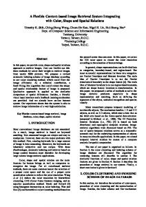
FLEXIBLE ADC: A DITHER AND OVERSAMPLING BASED SOLUTION TO IMPROVE THE PERFORMANCE OF ADC SYSTEMS (1)
J.M. Dias Pereira(1), A. Cruz Serra(2) and P. Girão(2) DSI, Escola Superior de Tecnologia, Instituto Politécnico de Setúbal, Portugal DEEC, Instituto Superior Técnico, Universidade Técnica de Lisboa, Portugal
(2)
Abstract: A well-known technique that can be used to increase the resolution of ADC digitising systems is based on dithering, oversampling and noise shaping. Dithering assures a uniform power spectral density for the quantisation error, oversampling. Followed by digital filtering, it improves signal to noise ratio and effective number of bits at the expenses of the input signal bandwidth. Noise shaping removes quantisation error power from signal bandwidth. The present paper introduces the concept of a flexible ADC that can be applied to an ordinary data acquisition board as a solution to optimise digitising systems performance for different sampling rates. Gains of ten or more effective bits can be obtained, for low frequency input signals, using always the maximum sampling rate of the ADC together with dithering, oversampling and noise shaping techniques. Keywords: Dither, Oversampling, Noise Shaping. 1
INTRODUCTION
Two main performance parameters in any digitising system are resolution and sampling rate. Unfortunately, sampling rate and resolution are usually competing interests in the design of any acquisition system, but for a single ADC system substantial gains in resolution can be obtained for input signals with low bandwidth compared with ADC sampling rate. In the present paper, dithering and noise shaping techniques are used together with oversampling to optimise the performance of an ADC based digitising system. Two different hardware configurations are considered to obtain a flexible ADC implementation: one based on a combination of an ADC and a digital signal processor (DSP) and another one based on an ordinary data acquisition board (DAQ) with external trigger and clock capabilities. In both configurations, the ADC is used in oversampling mode with a sampling rate equal to its maximum value. The overall digitising system behaves, from the view point of topology, as a multibit sigma-delta (Σ-∆) converter, which takes advantages of digital signal processing techniques to increment output signal-to-noise relation at the expenses of input signal bandwidth. Effective sampling rate of the output digitised signal is much lower than ADC sampling rate due to the usage of decimation, but its resolution varies inversely with the input signal bandwidth. Section 2 gives an overview of the basic concepts related to dithering, oversampling and noise shaping, highlighting the compromise between resolution and bandwidth for an oversampled ADC system, and introducing two different hardware solutions to implement the flexible ADC. Simulated and experimental results are presented in sections 3.1 and 3.2, respectively. Section 4 is dedicated to conclusions and future developments.
2
SYSTEM DESCRIPTION
Figure 1 represents two possible solutions for the hardware block diagram of a flexible ADC. One of the solutions (Figure 1(a)) is based on a DAQ board connected to a personal computer (PC) that performs filtering and decimation functions. Optional synchronisation between signal triggering and sampling can be provided by a phase locked loop (PLL) used as a frequency multiplier with a factor equal to the oversampling factor (N). In this case, external triggering and clock capabilities of DAQ board must be available. Another solution, represented in Figure 1(b), is based on a DSP whose fast on-chip, fixed or floating point, multiplier allows the device to perform fundamental digital signal processing operations, such as filtering and decimation, with optimum efficiency. Figure 2 represents the connections between the noise shaper block diagram and the flexible ADC. Noise shaping can be used to obtain additional reduction of quantisation error inside the signal bandwidth. The first order modulator, associated with the ADC, shapes the quantisation error power
density so that it lies above the passband of the digital output filter. The effective number of bits (ENOB) that can be reached is therefor much larger than would otherwise be expected from the oversampling ratio without noise shaping. Analogue input signal
PC
DAQ
∆fI
Σ
+
ADC
SC
Tr
(fS)
n FILT / DEC
FIFO
Ck
fS
N
-
fADC
PLL (÷ ÷N)
Nef
Digital output signal
Timer
NS
(a) Analogue input signal
DSP
∆fI
ADC
Σ
+
n
(fS) FILT / DEC
Tr Ck
-
fS
N
fADC PLL (÷ ÷N)
NS
Nef
Digital output signal
Timer
n fS≥2∆ ∆fI (Nyquist criteria) fADC=NfS
Figure 1.
(b)
Hardware block diagram of a flexible ADC: (a) using a data acquisition board and a PC; (b) using an ADC and a DSP (PC- personal computer; SC- signal conditioning circuits; PLL- phase locked loop; FILT- filtering; NS- noise shaping; DEC- decimation; FIFO- firstin first-out memory; Tr- trigger input; fADC- ADC sampling rate; ∆fI - input signal bandwidth; fs- effective sampling rate; N- oversampling factor). Analogue input signal
Digital output signal
Flexible ADC
Σ
+
ADC (n)
-
PC/DSP n
Nef DAC (m)
H(z)
-
Σ
+ NS
H(z)=z
Figure 2.
2.1
-1
m≥ ≥n
Connections between the noise shaper block diagram and the flexible ADC (NS- noise shaper; n- number of bits of the ADC; m- number of bits of the DAC).
Oversampling, filtering and dithering
The ADC sampling rate (fADC) is equal to its maximum value and the effective sampling rate (fS), taken from the PC or DSP, depends on the input signal bandwidth (∆fI). The effective number of bits (Nef) obtained after digital filtering varies in a logarithmic way with the oversampling factor (N) [1]:
1 N Nef = n + log2 2 2 1+ k
(1)
where n represents the number of bits of the ADC, k the normalised dither amplitude referred to the ADC quantisation step (Q), and the oversampling factor (N) is defined by the ratio between ADC sampling rate and Nyquist rate (fN) of the input signal, defined by:
fN = 2∆fI
(2)
where (∆fI) represents the input signal bandwidth. From (1) we conclude that for each additional effective bit we must increment the oversampling by a factor equal to four. Consequently, the relation between input signal bandwidth (∆fI) and ADC sampling rate (fADC) is given by the following expression:
ÄfI Äf 1 = I = 2 2(Nef − n) fADC NfS 2(1 + k )2
(3)
From the last expression we obtain the well known result that the input signal bandwidth is reduced to one quarter of its value for each additional effective bit gain when oversampling and filtering techniques are used. In order to assure a uniform power spectral density of the quantisation error [2], self-dithering provided by the noise naturally added to the signal and by the ADC internal noise is usually enough, considering that the amplitudes of those noise signals are adequate for dithering purposes. These noise signals are also assumed to be uncorrelated with the analogue input signal of the converter. If this is not the case, or if large-scale dithering is required to minimise ADC non-linearities [3], an additive or subtractive topology must be considered (Figure 3), and for the last case expressions (1) and (2) are still valid with k=0. For deterministic dithering with an auto-subtractive topology, dither subtraction is achieved without the need of an actual subtractor. The subtracting effect is maintained as long as the dither experienced by the input signal exhibits a zero mean value and the linear filter averages the digital output signal over an integer number of dither periods. Analogue input signal +
Digital output signal
Σ
Input signal
ADC +
+ PRN
DAC
Σ
ADC +
Σ PRN
DAC
(a)
+
Digital output signal
(b)
Figure 3. Dither insertion topologies: (a) additive or auto-subtractive; (b) subtractive (PRN- pseudo random noise ).
2.2
Noise shaping
Additional gains in effective number of bits, without so high bandwidth penalties, can be obtained with the usage of noise shaping techniques that remove quantisation error from signal bandwidth (base-band) to out-of-band, and is afterwards cancelled by filtering. Supposing that the quantisation error density is frequency independent in the band f=0 to f=fADC/2, the total noise power associated with the quantisation error for a first-order noise shaper (Fig. 2), after filtering, is given by [4]: fS /2
2
NQ = ∫ nq2 1 − e − j2ð f/fS df
(4)
0
2
where nq represents the power density of uniform quantisation error. Using Euler’s relationship and some trignometric equalities, the result of the integration represented by (4) is equal to:
Q2 1 1 ð NQ = 4 − sin 12 2N 2ð N
(5)
where Q represents the quantisation step of the ADC and N the oversampling factor previously defined. The signal-to-noise relation gain (SNRG) associated with filtering and noise shaping is given by:
Q2 /12 1 1 1 ð SNRG = = − sin NQ 4 2N 2ð N
−1
Using a third order Taylor series approximation for the function sin(x):
(6)
x3 sin(x) ≅ x − 6
(7)
it is possible to obtain:
1 1 1 SNRG = 4 2N 2
-1
p p3 3N3 = 3 2 ð N 6N ð
(8)
and using logarithmic units:
SNRG (dB) ≅ 30log10 (N) − 5.2 dB
(9)
From the last expression it is possible to confirm that for each duplication of the oversampling factor (∆N=2), the signal to noise relation gain (∆SNRG) is equal to 9 dB, which corresponds to a gain of 1.5 effective bits of the digitising system. This means that for the same oversampling factor (N>>1), the effective number of bits gain with noise shaping is three times higher than the one obtained with oversampling and filtering alone.
3
RESULTS EVALUATION
A LabVIEW simulator was developed to study global effects of oversampling, dithering and noise shaping techniques on signal digitalisation. Experimental results to confirm the effective number of bits gain as a function of the input signal frequency were obtained with a Keithley-Metrabyte data acquisition board (DAS4102) that has the following main characteristics: maximum sampling rate=64 MS/s; ADC number of bits: n=8 (flash type); ADC internal sampling rates: 0.5; 1.0; 2.0; 4.0; 8.0; 16.0; 32.0; 64.0 MS/s.
3.1
Simulation results
The main input parameters of the simulator are: oversampling factor (N), signal and noise amplitudes, dither characteristics – amplitude, period and type, number of bits (n) of the ADC, digitalisation options – filtering, decimation and noise shaping and sine wave curve fitting convergence parameters – maximum number of iterations and tolerance (maximum error). The main output parameters of the simulator are: sine wave interpolated signal, conversion error and effective number of bits of the digitised output signal. The four parameters (amplitude, frequency, initial phase and offset) least mean squares algorithm for sine wave fitting [5], using matrix operations, was fully implemented in LabVIEW. Non-linearity errors of the converter can also be easily added to the ADC model virtual instrument (VI). Figure 4 represents the front panel of the virtual instrument and in Figure 5 are presented simulator 4 16 results for an oversampling factor (N) between 2 and 2 , a six bit ADC (n=6) and a uniform dither component with the following characteristics: amplitude equal to 1 LSB (least significant bit) and period equal to 16.
Figure 4. Front panel of the LabVIEW virtual instrument used for simulation.
10
9
(4) 8
(3) 7
(1)
Nef (bits) 6
(2) 5
4
3
Figure 5.
4
5
6
7
8
9 10 log2(N)
11
12
13
14
Simulated results: (1)- without dither, filtering and noise shaping; (2)- with dither, noise shaping and no filtering; (3)- with dither, filtering and no noise shaping; (4)- with dither, filtering and noise shaping.
As main conclusions after several simulations it is important to refer that filtering and noise shaping techniques require a minimum value of oversampling factor in order to be effective (signal amplitude variation between samples less than 1 LSB); noise shaping advantage over filtering is only visible when 8 the oversampling factor is larger than a minimum value (in the example N=2 ). For each oversampling factor value there is a optimal value of dither period and amplitude that maximises digitising system performance.
3.2
Experimental results
Experimental results, represented in Figure 6, were obtained using a DAQ board from KeitlleyMetrabyte (DAS4102) and a sine wave generator with enough accuracy for an eight-bit converter (HP33120-A). Curve (a) represents the effective number of bits (ENOB) as a function of input signal frequency, assuming a maximum integer oversampling factor without application of noise shaping techniques. Curve (b) represents the same kind of data for an oversampling factor equal to an integer power of two. Finally curve (c) represents the effective number of bits (ENOB) as a function of input signal frequency, assuming a maximum integer oversampling factor equal to an integer power of two but with application of noise shaping techniques. Effective number of bits evaluation was based on the sine wave curve fitting algorithm (four parameters). Synchronisation between the external clock and triggering of the data acquisition board was provided by a phase locked loop (PLL) circuit. These results clearly show the advantages that can be obtained with the proposed method, especially when low frequency signals are present at the input of the digitising system. Nef (bits)
Nef (bits)
15 14
15 14
13
13
12
12
11
11
10
10
9
9
8
8
7
7
6
6 5
5 0
5
10
15
fI (MHz)
(a)
20
25
30
0
5
10
15
fI (MHz)
(b)
20
25
30
Nef (bits)
24 22 20 18 16 14 12 10 8 6 0
5
10
15
20
25
30
fI (MHz) (c)
Figure 6. Effective number of bits as a function of input signal frequency for an 8 bit converter: (a) maximum integer oversampling factor without noise shaping; (b) maximum integer power of two oversampling factor without noise shaping; (c) maximum integer power of two oversampling factor with noise shaping (continuous line – theoretical results; symbol ‘*’ – experimental results). Maximum relative difference between experimental and expected theoretical effective number of bits is lower than 5%. This difference can be explained taking into consideration the differential nonlinearity (DNL) and integral non-linearity (INL) errors of the DAQ board which are equal to 0.6 LSB, its maximum signal-to-noise relation equal to 46.3 dB (Nef=7.4), distortion of input signal generator and other errors associated with digital signal processing, like coefficient quantisation and truncation errors of digital filters.
4
CONCLUSIONS AND FUTURE DEVELOPMENTS
Simulated and experimental results show clearly the advantages of the proposed principle of the flexible ADC. The technique can be applied to an ordinary DAQ board and assures a complete usage of ADC performance for all effective sampling rates. Gain of 1.5 bits can be obtained for each doubling of oversampling factor (N). At the same time, usage of oversampling minimises the accuracy requirements of the sample-and-hold amplifiers, eases the design of antialiasing filters and minimises differential non-linearity errors (DNL) that are a serious problem for low amplitude signals [6]. Results obtained with the simulator, developed to study global effects of dithering, noise shaping, filtering and decimation, in the presence of input non-stationary signals, point out that for deterministic dither there is an optimum value of dither amplitude and period for each value of oversampling factor. As future developments of the present work, it will be considered an automatic selection of the oversampling factor based on the input signal frequency contents obtained using a FFT algorithm. This capability, together with the flexible ADC concept introduced in this paper, creates what we can call “smart ADC” with an automatic selection of resolution as a function of the input signal bandwidth.
REFERENCES [1] Jan Holub, Josef Vedral, “Dithered Quantizer of ADC Plug-In Card: Theoretical Model and Practical Testing”, XIV IMEKO World Congress, Vol.IVb, pp. 287-290, Tampere, Finland, June 1997. [2] Robert M. Gray, “Quantization Noise Spectra”, IEEE Transactions on Information Theory, Vol.36, No. 6, Nov. 1990. [3] Paolo Carbone, Claudio Narduzzi, Dario Petri, “Dither Signal Effects on the Resolution of Nonlinear Quantizers”, IEEE Transactions on Instrumentation and Measurement, Vol. 43, No. 2, pp. 139-145, April 1994. [4] Rudy van de Plassche, “Integrated Analog-to-Digital and Digital-to-Analog Converters”, Kluwer Academic Publishers, 1994. [5] Institute of Electrical and Electronics Engineers, Inc., “IEEE Standard for Digitizing Waveform Recorders, IEEE Std 1057-1994, pp. 35-36, December 1994. [6] Brad Brannon, “Overcoming Converter Nonlinearities with Dither”, Application Note 410 (AN-410), Analog Devices, 1996. AUTHOR(S): Adj. Prof. Dr. J.M. Dias Pereira, Departamento de Sistemas e Informática, Escola Superior de Tecnologia, Rua do Vale de Chaves, Estefanilha, 2910 Setúbal, Portugal, Tel. 351-265790000 Ext 6254, Fax 351-265-721869, E-mail:
[email protected]