The formal method of symbolic trajectory evaluation (STE) ap- pears to offer a solution, however. STE verifies that a circuit satisfies a formula in a carefully ...
Formal verification of PowerPCTM arrays using symbolic trajectory evaluation Manish Pandey1 1 2
Richard Raimi2
Derek L. Beatty2
School of Computer Science, Carnegie Mellon University Pittsburgh, PA 15213 Motorola Inc., 6501 William Cannon Drive West, Austin, TX 78735.
Abstract
of Boolean functions [4], and utilize the canonicity of OBDDs to determine equivalence. It is now common in the industry to simulate at the RTL level, and depend on such Boolean comparison tools to guarantee equivalence of lower-level implementations.
Verifying memory arrays such as on-chip caches and register files is a difficult part of designing a microprocessor. Current tools cannot verify the equivalence of the arrays to their behavioral or RTL models, nor their correct functioning at the transistor level. It is infeasible to run the number of simulation cycles required, and most formal verification tools break down due to the enormous number of state-holding elements in the arrays.
Arrays have not fit well into this strategy, however. Translating transistors into combinational logic and latches can fail to capture the complex timing in arrays. The state explosion problem poses a greater difficulty, however. Arrays contain enormous numbers of storage elements, and a Boolean comparison tool will naively attempt to build OBDDs of functions which depend on all the storage bits. This is usually not feasible.
The formal method of symbolic trajectory evaluation (STE) appears to offer a solution, however. STE verifies that a circuit satisfies a formula in a carefully restricted temporal logic. For arrays, it requires only a number of variables approximately logarithmic in the number of memory locations. The circuit is modeled at the switch level, so the verification is done on the actual design.
Recently, at the joint IBM-Motorola PowerPC microprocessor design center, Somerset, the formal verification technique of Symbolic Trajectory Evaluation (STE) has been applied to arrays. STE offers the following advantages:
We have used STE to verify two arrays from PowerPC microprocessors: a register file, and a data cache tag unit. The tag unit contains over 12,000 latches. We believe it is the largest circuit to have been formally verified, without abstracting away significant detail, in the industry. We also describe an automated technique for identifying state-holding elements in the arrays, a technique which should greatly assist the widespread application of STE.
1.
Randal E. Bryant1
1. Array properties can be verified using a number of variables approximately logarithmic in the number of array nodes, ameliorating the state explosion problem. 2. STE tools utilize switch-level simulation, allowing accurate modeling of actual transistor behavior. 3. Arrays usually have concise, well-understood specifications. STE tools can directly verify adherence of the transistor or RTL model to these specifications.
Introduction
In this paper we report on using Symbolic Trajectory Evaluation (STE) to verify on-chip memory arrays from PowerPC microprocessors. Arrays include circuits such as multi-ported register-files, instruction and data caches and cache tag units. These circuits typically consist of a Static Random Access Memory (SRAM) core embedded within complex logic. Such units are generally designed at the transistor-level and have non-trivial internal timing, including selftimed components.
We used the Voss STE system [11] in our work. Voss provides a powerful, functional language interface to the STE verifier, called FL. FL is a strongly-typed polymorphic functional language, similar to ML [9]. Voss represents Boolean functions with OBDDs, making Boolean function manipulation particularly fast and convenient.
2.
Verification of on-chip arrays has been a weakness in the verification strategies of many companies. Behavioral or RTL models of arrays are usually simulated as part of the full-chip verification effort. These simulation results then need to be related to the actual array implementations. In recent years, formal verification tools for comparing RTL models to gate level netlists have come into widespread use[7]. Most use Ordered Binary Decision Diagram (OBDD) representations
Preliminaries
STE [10] is a descendant of symbolic simulation [5]. A symbolic simulator propagates symbolic variables through a circuit network, in addition to logic constants. For symbolic simulation to be efficient, a compact format for Boolean functions is needed. The development of Ordered Binary Decision Diagrams (OBDDs) in the late 1980’s provided such a format [4]. With that advance came the desire to integrate symbolic simulation with a rigorous, formal proof procedure. Bryant and Seger developed the theory of Symbolic Trajectory Evaluation towards that end [10].
�
This research is sponsored by the Wright Laboratory,Aeronautical Systems Center, Air Force Materiel Command, USAF, and the Advanced Research Projects Agency (ARPA) under grant number F33615-93-1-1330 and in part by a grant from Motorola Inc. 0
In STE, properties of circuits are expressed in a restricted temporal logic. Formulae in the underlying logic can be simple predicates (e.g., ’node x is 1’) or conjunctions of these. Such formulae can be operated on by a next time operator (e.g., “node x is 1 on the next time step”), or qualified by domain restriction (e.g., “node x is 1 when function E is true”). These latter are also formulae. An assertion is an implication between two formulae. 1
WADR0[0:4] DIN0[0:31] WE0
WRITE PORT 0
R0 R1 R2 R3 R4
WADR1[0:4] DIN1[0:31] WE1
WRITE PORT 1
R31
WRITE INHIBIT TGPR_WR
TR0
TGPR_RD READ_CLK WRITE_CLK
READ PORT 0
READ PORT 1
READ PORT 2
READ PORT 3
TR3 READ PORT 4
RADR0[0:4] DOUT0[0:31] RE0 RADR1[0:4] DOUT1[0:31] RE1 RADR2[0:4] DOUT2[0:31] RE2 RADR3[0:4] DOUT3[0:31] RE3 RADR4[0:4] DOUT4[0:31] RE4
INDEX[0:6] LOAD_REQ STORE_REQ SNOOP_REQ
set0 set1 set2
tag0
vm
tag1
vm
tag2
vm
tag3
v m LRU
tag0
vm
tag1
vm
tag2
vm
tag3
v m LRU
tag0
vm
tag1
vm
tag2
vm
tag3
v m LRU
set127
tag0
vm
tag1
vm
tag2
vm
tag3
v m LRU
RESET other control signals TAGIN[0:19]
4-way COMPARATOR + LOGIC
STAT[0:1] WW[0:1] LRU UPDATE
CLK1 CLK2
HIT HITWAY[0:1] DIRTY TAGOUT[0:19]
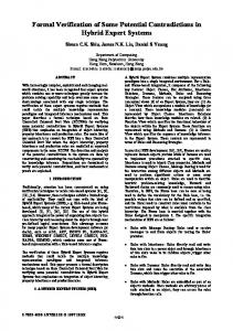
Figure 1: Multi-ported Register File Unit.
Figure 2: Data Cache Tags Unit
STE provides an algorithm for proving such assertions valid. It is a model-checking algorithm, in that it checks whether a system is a model of an assertion in the logic. However, it should not be confused with CTL model-checking [6]. STE lacks the expressiveness of CTL, e.g., eventuality properties are not expressible, nor is existential path quantification available. Use of STE is limited to applications wherein the properties to be verified are expressible in its (rather limited) logic, and, in addition, the set of starting states for the verification can be safely assumed to be reachable states. Unlike CTL model-checkers, STE tools do not calculate the reachable state set of a circuit. For arrays, these restrictions are acceptable. It is generally sound to assume that array nodes can hold arbitrary bit combinations. And, even in cases where this is not so, the state invariants can usually be manually derived and the array properties verified under these invariant conditions. Additionally, the behavior of memories can generally be expressed in the STE logic.
the WRITE CLK signals are mutually exclusive. The environment guarantees that the two write addresses are always different.
���� �
To use STE, properties of circuits are expressed as assertions of the form , where A is termed the antecedent, and C the consequent. Intuitively, the antecedent defines initial settings and input stimuli, while the consequent defines expected results. The symbolic simulation engine simulates the symbolic patterns of the antecedent, and simulation results are compared to the consequent. The intuitive sense of STE is that it proves that the behavior exhibited by symbolic simulation of the antecedent is one of the possibly many behaviors consistent with the consequent, proving this for any assignment of values to the variables involved. The reader is referred to [10] for more detail.
3.
PowerPC array circuits
The first circuit we verified was a relatively simple multi-ported register file unit of a PowerPC microprocessor. The second circuit is the tags unit for a data cache circuit from a recent PowerPC design.
3.1.
Multi-ported register file
Figure 1 shows a high-level view of the register file, which has 2 identical write ports and 5 identical read ports. When READ CLK is high, the register file does a read operation and when WRITE CLK is high, the register file does a write operation. The READ CLK and
The register file contains 36 registers of 32 bits each, arranged in two banks, R0-R31 and TR0-TR3. During a write operation, when TGPR WR is low, the writes go to one of R0-R31 as specified by the 5-bit address for each write port. When TGPR WR is high, the writes go to one of TR0-TR3 based on the two least significant address bits. The environment is supposed to keep the middle address bit (bit 2) at 0, when the TGPRs are to be written. WRITE INHIBIT when high prevents any writes from occurring. Also, each port has a write enable signal (WE0, WE1). The read ports also have read enable signals (RE0,..., RE4). When TGPR RD is low, the five address bits select a register from the first bank. When TGPR RD is high, the lowest two address bits select a register from the second bank, and bit 2 of the address must be low for the read to be successful. If a read does not occur on a port, or if bit 2 of the address is high when TGPR RD is high, then the port’s data output stays precharged high.
3.2.
Data cache tags unit
The data cache tags (DTAG) circuit, shown in figure 2, contains 128 4-way-associative sets. Each set contains 4 tags of 20 bits each, and each tag has one valid and one modified (dirty) bit. Also, each set contains 6 least-recently-used (LRU) bits which record the access history of its four ways. In a typical operation, a 7-bit index at the INDEX input selects one of the 128 sets, and the 20-bit tag at TAGIN is compared in parallel with all four tags in the selected set. If a tag matches, then the HIT signal goes high and the LRU bits are updated to reflect that the matched way is most recently used. HITWAY indicates which of the four ways is hit. If none of the four tags match, the HIT signal remains low, and the least recent tag appears at TAGOUT (for cache replacement). Other important operations are the reset and the tag write operations. In the reset operation, the RESET signal resets the DTAG unit by zeroing all valid, modified and LRU bits. In the tagwrite operation, the tag value at TAGIN and the valid and modified bit values at STAT are written into a way selected by WAYSEL of a set specified by SLOW INDEX.
CIRCUIT NODE
�
ASSERTION PHRASE
NODE VALUE and TIMING
READ_CLK
Register R i
u
Register R j
v
(R[i]=u) in antecedent (TR[n]=v) in antecedent
(antecedent)
i
RADR0
(ReadAdr0=i)
EN0
(ReadEn0=1)
TGPR_RD
(TGPRRead=0) u
DOUT0
(Dout0=u)
Register R i
u
Register R i
v
(consequent) (consequent)
(R[i]=u) in consequent (TR[n]=v) in consequent
��
Each abstract assertion is a symbolic expression of the form LEADSTO
Antecedent Consequent. The Antecedent specifies the current state of the abstract machine and the current inputs. The Consequent specifies what the outputs and new state of the machine should be, after the abstract machine makes a transition. For example, the abstract assertion for a read operation at port 0 of the register file (see Section 3.1) is
�
�����
0
�
�� ��
����
#"$���
���&%(' �
�
�
� ��� ��� ������ !)��
0
���
� �
� ��� ��� ������
���
��
�
��� ��� �� ���
�� ��� �
� �&��
�*(�
0
1
�
(1) (2)
LEADSTO
���
��� ��� �� ���
��+ , �-� � � #"$� ��.0/ �21
0
��2�3�
�
�
"
�
In verifying the arrays, we structured our specifications into 2 parts: a set of high level assertions over an abstracted system state, and an implementation mapping that relates that abstracted state to circuit state. The set of assertions is defined by the set of operations that the array can perform. Each assertion gives the conditions required for doing one operation, and the conditions guaranteed as a result of it. The implementation mapping converts the abstracted state into constraints on signals in the circuit over time. Structuring specifications in this way keeps the most critical part of the specification—the abstract description of the desired behavior—simple, clear, and free of implementation-specific details. This methodology [1, 2] is not directly supported by Voss. However, we disciplined our use of the FL language to write our specification in a hierarchical manner and separated the abstract assertions from the implementation mapping.
�!
The implementation mapping, illustrated in figure 3, expands such an assertion to include details of the circuit implementation, such as the timing of state, IO, and clock signals. It maps the value of each � ��
�! component of the abstract state (for example, 0) onto the values of one or more specific��/=circuit nodes at specific times. For � >� ��
�� in the abstract assertion example, the figure shows how translates to the READ CLK signal making low to high and then high to low transitions during specified times, and the WRITE CLK signal staying low. �
Verification methodology
� � ��
4
Note that the variables , , and in the assertion are used as array indices. The implementation mapping represents each of them in binary form as a word of symbolic Boolean variables. From the �(�?�@� A� , the implementation mapping will iniantecedent fragment tialize each RAM storage node B in the register file with a symbolic ternary function
Figure 3: Implementation mapping for the register-file.
4.
�
�
(op = Read)
WRITE_CLK (antecedent)
"
initially, after a read operation at some address , still contains . In line 4, we verify that the read operation results in the correct �:4 � data value being sent to the output. When contains , and the " � read address is , we are interested in checking the output for data , � � ;"$� + , �