Framework for Application Mapping over Packet-switched Network of FPGAs : Case studies Vinay B. Y. Kumar∗ , Pinalkumar Engineer∗ , Mandar Datar∗ , Yatish Turakhia† , Saurabh Agarwal∗ , Sanket Diwale‡ and Sachin B. Patkar∗ Department of Electrical Engineering, Indian Institute of Technology Bombay, Mumbai, India Email:∗ {vinayby, pje, mandardatar, saurabh, patkar}@ee.iitb.ac.in, †
[email protected], ‡
[email protected] applications/algorithms (used interchangeably henceforth)— particularly those amenable to be expressed in a data-flow manner—through a network abstraction, and an automation framework that would simplify exploration of this complex design space in mapping to a given multi-FPGA platform. In particular, we map the application task graph to a packetswitched Network-on-Chip (NoC), and extend the NoC abstraction across FPGAs communicating over quasi-serial links. The path from a higher-level specification of the application to a task-graph with precedence constraints, followed by coarsening and identifying the partition across chips is not discussed in this work (related earlier work: [4]). We illustrate the framework through three cases studies that could use scalability, each of a different flavor—I. LDPC decoding, min-sum algorithm; II. Particle Filter based Object Tracking; and III. Matrix Vector Multiplication over GF(2). Case I naturally has a message passing structure, unlike II. For case III, although a more straightforward message passing model could have been used, as a way to highlight the role of a domain expert in this step, we use a novel sub-quadratic algorithm by Ryan Williams [5], this incidentally being its first hardware realization. For each case study, in phase-1, we
Abstract—The algorithm-to-hardware High-level synthesis (HLS) tools today are purported to produce hardware comparable in quality to handcrafted designs, particularly with user directive driven or domains specific HLS. However, HLS tools are not readily equipped for when an application/algorithm needs to scale. We present a (work-in-progress) semi-automated framework to map applications over a packet-switched network of modules (single FPGA) and then to seamlessly partition such a network over multiple FPGAs over quasi-serial links. We illustrate the framework through three application case studies: LDPC Decoding, Particle Filter based Object Tracking, and Matrix Vector Multiplication over GF(2). Starting with highlevel representations of each case application, we first express them in an intermediate message passing formulation, a model of communicating processing elements. Once the processing elements are identified, these are either handcrafted or realized using HLS. The rest of the flow is automated where the processing elements are plugged on to a configurable network-on-chip (CONNECT) topology of choice, followed by partitioning the ‘on-chip’ links to work seamlessly across chips/FPGAs.
I. I NTRODUCTION As applications targeting FPGAs grow more pervasive or when they need to scale, there are matching demands on logic capacity as well as resources such as special-function on-chip resources, I/O and reliable multi-gigabit transceivers. Moore scaling enabled meeting these demands in large part. As with general purpose processors, more than Moore scaling with FPGAs is enabled by multiple FPGA platforms—the classic use-cases of which are ASIC prototyping, Emulation and Hardware-acceleration of applications and also more recently for datacenter applications [1]. Although commercial HLS tools such as Vivado [2]— given good user directives—are capable of producing hardware of quality comparable to handcrafted designs, it is not within the ready scope of HLS tools to address the issue of scalability. This problem becomes even more tricky because of the fragmentation in the ways the multi-FPGA platforms are built, particularly in terms of the variety in the nature of host to FPGA/s and inter FPGA links, and underlying custom interfaces. Dally et. al. [3] recently advocated for design productivity through modular designs with standardized interfaces on a network-on-chip abstraction. In the current context, such a standard interface can abstract the variety in the physical links. In this work we begin to explore the scalability of Copyright is held by the author/owner(s). 2nd International Workshop on FPGAs for Software Programmers (FSP 2015), London, United Kingdom, September 1, 2015.
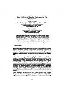
Design Entry Algorithm/Software
MultiFPGA Design Flow HW Acceleration Platform Parameters
(Re)Model in a Message Passing Framework Model Level Design Space Exploration Communication vs. Computation (PEs) Network parameters PE Clustering, Mapping
Design Mapped
FPGA aware NOC Generator MultiFPGA NOC Partitioner Processing Element Actualization Custom HW Design High−level Synthesis Compiled Code
Algorithm/MultiFPGA
Fig. 1: Design flow: Scaling Hardware Acceleration start with a high-level description of the algorithm, express it in message passing formulation, followed by realization of the processing elements either by HLS (Vivado) or custom design. Phase-2 automates the process of integrating these processing
22
Sequential Code
elements onto a network-on-chip (NoC) architecture (autogenerated by a NoC Generator, CONNECT [6]), followed by seamlessly (in a manner oblivious to the designer) partitioning the NoC over multiple FPGAs where the NoC links crossing FPGAs are replaced by stitching-in quasi-serial links implemented over FPGA pins. In other words, this work flow expects the algorithm domain expert (software) to help express the original algorithm in a message passing model (phase-1), the rest of the flow is an automation that gives a scaled design over an NoC or multiple FPGAs. Figure 1 outlines the design flow. This semi-automated framework is a work in progress, and was done with a little manual intervention for the case studies discussed.
Frontend Parsing
DFG Partitioning
Unified Scheduling and Mapping
Partitioned DFG Scheduling
Mapped + Scheduled DFG Code Generation
Synthesizable Base Templates
Assembly Like Code
(NOC + MIPS PROCESSORS) System Generation
Synthesizable Verilog
Fig. 2: Basic application partitioning and mapping tool flow
A. Organization The rest of the paper is organized as follows. Section II discusses phase-1 of the automation where the algorithm is expressed in a way that helps identification and synthesis of processing elements, followed by wrapping them with suitable adapters before plugging them to CONNECT NoC. Section III, phase-2 of the automation, describes the design of quasiSERDES endpoints and the automation of partition of the NoC across multiple FPGAs. The next three sections IV, V, and VI discuss the specific case studies mentioned above.
processing module is the basic processing element that is synthesized out of the processes/functions from the previous step. outgoing flit
incoming flit DATA COLLECTOR
DATA DISTRIBUTOR
DATA PROCESSING
II. P HASE -1: A PPLICATION MAPPING TO N O C A. Message passing modeling of the Application
Fig. 3: Structure of Processing elements connecting to NoC
The algorithm should first be expressed in a message passing formulation. This modeling, at the software level, is best done by the domain expert. The result is a model of software threads—corresponding to processing elements in hardware— communicating in a message passing fashion. For simplicity, we assume the body of the function/thread is executed after all the argument messages on received. 1) Note on compiler-driven automation: This phase too can be automated as long as the domain expert annotates the input high-level description appropriately. We have a compilerdriven toy automation flow (Figure 2) for this task, that partitions the Dataflow-Graph (DFG) extracted from a highlevel description (straight line code) to be executed on a network of MIPS processors. The DFG parts are compiled to a minimal MIPS instruction set with network-push/pull instructions (FIFO-semantics) added to account for the communication between the DFG parts, taking into account the precedence constraints/schedule. [4] is a follow-up work in this direction focusing on fast scheduling and mapping.
incoming flit
outgoing flit
start input FIFOs
done
DATA COLLECTOR
output FIFOs
(a) Data Collector module start input FIFOs
DATA DISTRIBUTOR
(b) Data distributor module
done output FIFOs DATA PROCESSING
(c) Computing elements for data processing
Fig. 4
B. Processing Element Realization and Interfacing to NoC Data collector and Data distributor modules—interfacing an NoC router on one side—are responsible for enabling external communication for processing elements over the NoC. Incoming data (in terms of Flits: basic units of data on NoC links) to the processing element is accepted at the router and processed by the Data Collector module, even with the flits arriving in an out-of-order fashion, and is put in appropriate
The hardware modules corresponding to the nodes of the message-passing graph identified in the previous step could either be designed by hand or a HLS tool. However, at this stage these modules are not yet network/NoC aware. Figure 3 shows the structure of a processing element that makes it pluggable on to an NoC. It consists of three modules: Data collector, Data processing and Data distributor. The Data
23
FIFOs corresponding to the input arguments of the processing element, the Data processor. Internal structure of Data Collector module is shown in Figure 4a. Once all the data is received and written into FIFOs, start is asserted to Data processing module. The interface of the Data processing module should be as in Figure 4c. Here, as the start is asserted, the input data is read from the input FIFOs, and once the computation is complete, the results are stored into output FIFOs and done is asserted. Data distributor module, as shown in Figure 4b, prepares the flit data (packet) from results and sends it to network interface of NoC router. 1) Automation: As mentioned earlier, the basic processing module could be designed using Verilog HDL or HLS. A script then generates a wrapper around such processing module in form of Data collector and Data distributor modules. Storage requirements of both input and output memory modules should be known a priori.
FPGA 1 N2
N2
N3
R2
N3
R2
R3
R3
Partitioning
N1
N1
N0
R1
R1
R0
N0
R0 FPGA 2
Fig. 5: Example 2-FPGA partition of an NoC
[To be SERIALIZED] Flit/Data from Router (input)
[DESERIALIZED] Flit/Data to Router (output)
Transmission Clock (input) Design Clock (input)
III. P HASE -2: PARTITIONING N O C ACROSS MULTIPLE FPGA S
p-bit Serialized Data (input)
We use a freely available web-based synthesizable RTL generator for the Network-on-Chip (NoC) infrastructure, named CONNECT (Configurable Network Creation Tool). CONNECT [6] can be used for generating NoCs of arbitrary topology and supports a large variety of router and network configurations. Also, CONNECT incorporates a number of useful features fine-tuned for the FPGA platform. In extending the NoC links across FPGAs, we require asynchronous links. However, the limited number of pins per FPGA would not support the typical router port-widths and radix counts. We therefore use serializer/deserializer (SERDES) blocks at the interfaces. One would typically use the dedicated multi-gigabit transceiver resources on the FPGA for SERDES links, but for this work, we develop a generic interfacing module that uses the GPIO pins available on any FPGA. As we use more than 1-pin to serialize the flit-transactions across a link (depending on the radix of the router, and the number of pins available), we call them quasi-SERDES. Assuming an 8-wire physical link, these quasi-SERDES modules (on either side of a link) implement the following protocol—whenever a valid data (valid bit in the flit) in presented as input from router keep it in buffer and start sending 8 bits at a time with MSB first; similarly, whenever a valid 8 bit MSB is received reconstruct output data and put the data on the output port to the router. Figure 5 shows an example partition of an NoC with four routers on two FPGAs. The router R0 (along with its processing element N0) is mapped onto a separate FPGA. Communication between FPGAs takes place using serializer/deserializer (quasi-SER/DES) links. The processsing elements N 1, 2, 3, 4 here are as constructed earlier.
Global Reset
quasi-SERDES ENDPOINT
Transmission Clock (output) p-bit Serialized Data (output) p-physical wires
Fig. 6: Quasi-SER/DES Link Endpoint
script automates the process of generating required number of independent parts of the NoC and inserting a pair of quasiSERDES endpoints on each NoC link cut. The independent part modules of the NoC are synthesized separately and programmed on respective FPGA boards. We have tested this framework between two Altera DE0-Nano boards, as well as two Xilinx Zynq Zedboads (ARM+FPGA).
IV. C ASE S TUDY: LDPC D ECODING
Listing 1 shows an outline of LDPC decoding based on the popular Min-sum algorithm. Number of data bits, to be decoded is N and N iters is maximum number of iterations for LDPC decoding. Input to LDPC decoder is initial LogLikelihood Ratio (LLR) of the data. LDPC decoding is done through Check nodes and Bit nodes iteratively, by passing message through dedicated channels between the nodes. Number of channels and interconnection between nodes depends on type of LDPC code. Here, we are using finite projective geometry based LDPC code [7][8] in GF (2, 2s ) with s = 1. The message passing model is evident for this application and the processing nodes (the bit and check nodes) are also readily identified.
A. Automation Given an NoC topology and an application mapped to it (as described above), and the decisions (presently user specified) as to ‘cuts’ that specify a partition on the NoC, an python
24
1 2 3 4 5 6 7 8 9 10 11 12 13 14 15 16 17
Control Unit
Listing 1: Outline of min-sum LDPC decoding d e c o d e d [N] = minsum ( d a t a [N] , N i t e r ) { do { f o r ( i = 0 ; i < N ; i ++) { / / I n i t i a l LLR v a l u e s u0 ( i ) = d a t a ( i ) ; u i j = i n i t i a l LLRs s e n t t o Check node / / j i s d e g r e e o f LDPC n o d e s
start
done
/ / Check node p r o c e s s i n g v i j = minimum ( u i j ) ; / / B i t node p r o c e s s i n g [ u i j , sum ] = sum ( v i j ) ;
C3
R14
R9
B2
d e c o d e d [N] = s i g n ( sum ) ;
B6
B4
R8
} } w h i l e ( i t e r a t i o n s