module. Inputs to the processor array architecture consist of a stream of residues, ...... Challenging the dogma: the hidden layer of non-protein-coding RNAs in.
Hardware-Accelerated RNA Secondary-Structure Alignment James Moscola and Ron K. Cytron Department of Computer Science and Engineering Washington University, St. Louis, MO and Young H. Cho Information Sciences Institute University of Southern California
The search for homologous RNA molecules—sequences of RNA that might behave simiarly due to similarity in their physical (secondary) structure—is currently a computationally intensive task. Moreover, RNA sequences are populating genome databases at a pace unmatched by gains in standard processor performance. While software tools such as Infernal can efficiently find homologies among RNA families and genome databases of modest size, the continuous advent of new RNA families and the explosive growth in volume of RNA sequences necessitate a faster approach. This work introduces two different architectures for accelerating the task of finding homologous RNA molecules in a genome database. The first architecture takes advantage of the tree-like configuration of the covariance models used to represent the consensus secondary structure of an RNA family and converts it directly into a highly-pipelined processing engine. Results for this architecture show a 24× speedup over Infernal when processing a small RNA model. It is estimated that the architecture could potentially offer several thousands of times speedup over Infernal on larger models, provided that there were sufficient hardware resources available. The second architecture is introduced to address the steep resource requirements of the first architecture. It utilizes a uniform array of processing elements and schedules all of the computations required to scan for an RNA homolog onto those processing elements. The estimated speedup for this architecture over the Infernal software package ranged from just under 20× to over 2, 350×. Categories and Subject Descriptors: C.1.3 [Processor Architectures]: Other Architecture Styles; J.3 [Life and Medical Sciences]: Biology and genetics General Terms: Algorithms, Design, Performance Additional Key Words and Phrases: Bioinformatics, RNA, Secondary-Structure Alignment
1.
INTRODUCTION
In the field of bioinformatics, sequence alignment plays a major role in classifying and determining relationships among related DNA, RNA, and protein sequences.
Permission to make digital/hard copy of all or part of this material without fee for personal or classroom use provided that the copies are not made or distributed for profit or commercial advantage, the ACM copyright/server notice, the title of the publication, and its date appear, and notice is given that copying is by permission of the ACM, Inc. To copy otherwise, to republish, to post on servers, or to redistribute to lists requires prior specific permission and/or a fee. c 2008 ACM 1529-3785/2008/0700-0001 $5.00
ACM Transactions on Computational Logic, Vol. V, No. N, December 2008, Pages 1–44.
2
·
James Moscola et al.
Sequence alignment is very well studied in the areas of DNA and protein analysis, and many tools have been developed to aid research in these areas [Altschul et al. 1990; Pearson and Lipman 1988; HMMER ]. However, only recently has the importance of non-coding RNAs (ncRNAs) been discovered [Storz 2002]. An ncRNA is an RNA molecule that is not translated into a protein, but instead performs some other cellular process. Examples of ncRNA molecules include transfer RNAs (tRNAs) and ribosomal RNAs (rRNAs). These molecules are typically single-stranded nucleic acid chains that fold upon themselves to create intramolecular base-paired hydrogen bonds [Durbin et al. 1998]. The result of these bonds is a complex three-dimensional configuration (shape) that partially defines the function of an RNA molecule. This configuration is known as the secondary structure of the RNA molecule. Two molecules are said to be homologous if they have similar to identical secondary structures. Homologous RNA molecules are likely to have similar biological functions, even though they may have dissimilar primary sequences. For example, the primary sequence AAGACUUCGGAUC creates the secondary structure shown in the left portion of Figure 1(b). A homologous molecule with a highly dissimilar primary sequence could result from exchanging the sequence’s G and C nucleotides, or by substituting U for C and A for G. The DNA sequences from which ncRNA molecules are transcribed are known as RNA genes. However, unlike protein-coding genes, RNA genes cannot be easily detected in a genome using statistical signals [Rivas and Eddy 2001]. Moreover, because related RNA genes tend to exhibit poor primary sequence conservation, techniques developed for comparing DNA sequences are ill-suited for detecting homologous RNA sequences [Durbin et al. 1998]. Instead, techniques have been developed that utilize the consensus secondary structure of a known RNA family to detect new members of that family in a genome database [Eddy and Durbin 1994]. To date, these techniques have proven to be very computationally complex and can be quite demanding even for the fastest computers [Eddy 2006]. The consensus secondary structure of an RNA family can be represented as a stochastic context-free grammar (SCFG) that yields high-probability parses for, and only for, the primary sequences of molecules belonging to the family [Searls 1992]. Several tools have been developed that employ SCFGs as a means of detecting homologous RNA molecules in a genome database. At the forefront of these tools is the Infernal software package [Infernal ] and the Rfam database [Griffiths-Jones et al. 2005] which currently includes SCFGs for over 600 RNA families. Infernal has shown great success in its ability to detect homologous RNA sequences in genome databases. Additionally, since it was first released in 2002, Infernal has been frequently updated and extended to incorporate various heuristics to decrease the computational costs of finding homologous RNA sequences [Weinberg and Ruzzo 2006; Nawrocki and Eddy 2007]. However, even with these improvements, the time to scan a large genome database can still take many hours, days, or even years, which greatly limits the usefulness of tools such as Infernal. This work examines architectures for finding RNA homologs using custom hardware. First, Section 2 presents related work. Next, Section 3 provides a brief background on the techniques used to model RNA secondary structures and the ACM Transactions on Computational Logic, Vol. V, No. N, December 2008.
Hardware-Accelerated RNA Secondary-Structure Alignment
·
3
algorithms used for finding homologous sequences in a genome database. Section 4 presents a highly-pipelined initial architecture that is capable of scanning genome databases at very high speeds. Although extremely fast, the resource requirements for the baseline architecture prohibits the architecture from practical use for even average size RNA models. In Section 5, a more practical architecture for scanning genome databases is presented that involves scheduling computations onto a set of parallel processing elements. One possible scheduling technique for use with this architecture is presented in Section 6. Finally, an analysis of the architecture is presented in Section 7. 2.
RELATED WORK
While heuristics [Brown 2000; Lenhof et al. 1998; Lowe and Eddy 1997; Weinberg and Ruzzo 2004; 2006; Nawrocki and Eddy 2007] can dramatically accelerate the computationally complex process of detecting homologous RNA sequences in genome databases, the completeness and quality of the results are often sacrificed. For example, some heuristics pre-filter sequences based on their primary sequence similarity, applying the more complex secondary structure alignment algorithms only on the sequences that pass the filter [Weinberg and Ruzzo 2004; 2006]. However, because these filters are based on the consensus primary sequence of an RNA family, they do not work well on families that have limited primary sequence conservation [Nawrocki and Eddy 2007]. Furthermore, as an RNA family grows, and more variation is introduced into the consensus primary sequence, these filtering techniques may become ineffective. Concurrency can also be exploited to improve performance. Liu and Schmidt [Liu and Schmidt 2005] utilized coarse-grained parallelism and a PC cluster to achieve a 36× speedup. While not directly related RNA secondary structure alignment, Aluru [Aluru et al. 2003] and Schmidt [Schmidt et al. 2002] present approaches for taking advantage of finer grained parallelism in primary sequence comparisons. 3.
BACKGROUND
Transformational grammars were first described as a means for modeling sequences of nucleic acids by Searls [Searls 1992]. Grammars provide an efficient means of modeling the long range base-pair interactions of RNA secondary structures. More specifically, stochastic context-free grammars (SCFGs) provide the framework required to represent probabilistic models of both the primary sequence and the base-paired secondary structure of an RNA molecule. Given a multiple sequence alignment of an RNA family, one can construct a profile-SCFG, also referred to as a covariance model (CM), that can subsequently be used to detect homologs in a genome database [Eddy and Durbin 1994]. The remainder of this section provides background on CMs and how they are used for scanning genome databases. 3.1
Covariance Models
A covariance model (CM) is a specialized SCFG developed specifically for modeling both the primary sequence and secondary structure of RNA families. Figure 1 shows the development of a CM as follows. In Figure 1(a), three RNA sequences are aligned, with connected boxes showing the consensus base pairs that bind to ACM Transactions on Computational Logic, Vol. V, No. N, December 2008.
·
4
James Moscola et al.
(a) a
a
g
a
c
u
u
c
g
g
a
u
c
u
g
g
c
g
a
c
a
c
c
c
u
a
c
a
c
u
u
c
g
g
a
u
g
a
c
a
c
c
a
a
a
g
u
g
a
g
g
u
c
u
u
c
g
g
c
a
c
g
g
g
c
a
c
c
a
u
u
c
1
5
10
15
20
(b)
(c) a
a
1
5
MATL1
2
MATL2
c
a
u
c
u u
15 g
a g 10 g c
ML52
MR53
D54
IL55
IR56
MATP17
BIF3
u g
MP51
24
ROOT0
1
MATP16
(d)
MP57
c 24
g
c
g
c
c a
BEGL4
c 20
13
14 MATL15
4 MATP6
12
15 MATP16 24
MATR7
11
16 MATP17 23
5 MATP8
10
17 MATL18
6
MATL9
MR59
D60
BEGR14
3 MATP5
a
ML58
IL61
IR62
MATL18
18 MATP19 22
7 MATL10
19 MATL20
8 MATL11
20 MATL21
9 MATL12
21 MATL22
END13
END23
ML63
D64
IL65
Fig. 1: A reproduction of an example CM from [Durbin et al. 1998; Nawrocki and Eddy 2007]
form the secondary structure; the top sequence’s secondary structure is called out in Figure 1(b). The consensus secondary structure of all three sequences is represented by the directed binary tree in Figure 1(c), whose nodes indicate the binding pattern of the sequences’ nucleotides. While the three sequences of Figure 1(a) fit identically onto the binary tree, other sequences may fit the model only if appropriate insertions and deletions are applied. Such edits are accommodated by state transitions within a node. For three nodes of the binary tree in Figure 1(c), Figure 1(d) shows those nodes’ internal states and possible transitions. State Type MP M L / IL M R / IR B D S E
Description Pair Emitting Left Emitting Right Emitting Bifurcation Delete Start End
Production P → x i Y xj L → xi Y R → Y xj B → SS D→Y S→Y E→ǫ
Emission ev (xi , xj ) ev (xi ) ev (xj ) 1 1 1 1
Transition tv (Y ) tv (Y ) tv (Y ) 1 tv (Y ) tv (Y ) 1
Table I: Each of the nine different state types and their corresponding SCFG production rules
For the purposes of assessing the fitness of an RNA string for membership in an RNA family, the RNA string is parsed using grammar rules that model state transitions such as those in Figure 1(d). Each state can be represented as a SCFG production rule that has the form of one of the nine non-terminal (or state) types shown in Table I. Each state has its own set of emission probabilities for each of the single or base-paired residues that can be emitted from that state. Additionally, each state has its own set of transition probabilities for the set of states to which it can transition. ACM Transactions on Computational Logic, Vol. V, No. N, December 2008.
Hardware-Accelerated RNA Secondary-Structure Alignment
·
5
A state that is denoted as an M P state generates (or emits) the base-pair (xi ,xj ) with some emission probability ev (xi , xj ) and transitions to some state Y with some transition probability tv (Y ). Likewise, a state that is an M L (or IL) state generates (or emits) the single residue xi with some emission probability ev (xi ) and transitions to some state Y with some transition probability tv (Y ). The B type bifurcation states represent a fork in the tree structure of the CM and always transition to two distinct S type states without emitting any residues. S states are also members of the ROOT node of the CM. A D type state is used to represent a residue that is part of the CM, but missing from the target genome sequence. Leaf nodes of the CM are represented as E states and do not emit any residues. For a more detailed discussion on CMs, refer to [Durbin et al. 1998; Eddy and Durbin 1994]. 3.2
Rfam Database
An online database, known as the Rfam database [Griffiths-Jones et al. 2005], currently contains multiple sequence alignments and CMs for over 600 RNA families. Rfam is an open database that is available for all researchers interested in studying algorithms and architectures related to RNA homology search. Since its inception, the Rfam database has seen continuous growth as more ncRNA families are identified. Figure 2 depicts the growth of the Rfam database over the last five years. Estimates suggest that there are several tens of thousands of ncRNAs in the human genome [Mattick 2003; Washietl et al. 2003]. The vast number of ncRNAs suggests the need for a high-performance alternative to software approaches for homology search.
800
Number of CMs in Rfam DB
700 600 500 400 300 200 100
00 7 De c-2
Ju n-2 00 7
De c-2 00 6
Ju n-2 00 6
De c-2 00 5
Ju n-2 00 5
00 4 De c-2
Ju n-2 00 4
00 3 De c-2
Ju n-2 00 3
De c-2 00 2
Ju n-2 00 2
0
Fig. 2: The number of covariance models in the Rfam database has continued to increase since its initial release in July of 2002. ACM Transactions on Computational Logic, Vol. V, No. N, December 2008.
6
·
3.3
Database Search Algorithm
James Moscola et al.
CMs provide a means to represent the consensus secondary structure of an RNA family. This section describes how to utilize a CM to find homologous RNA sequences in a genome database. Aligning an RNA sequence to a CM can be implemented as a three-dimensional CYK (Cocke-Younger-Kasami) [Cocke 1969; Younger 1967; Kasami 1965] dynamic programming (DP) parsing algorithm. Each state in the CM is represented as a two-dimensional matrix with rows 0 through L where L is the length of the genome database, and columns 0 through W where W is the length of the window (i.e. the longest subsequence of the genome database) which should be aligned to the CM. Figure 3 shows an example of the alignment window as it scans across a genome database. Genome Database L = 25
: A.C.U.G.U.A.G.C.U.G.C.U.G.A.C.U.G.A.U.G.C.U.A.G.C Alignment Window W=5
Fig. 3: An alignment window scans across the genome database. Each window is aligned to the CM via the DP parsing algorithm.
The DP algorithm initializes the three-dimensional matrix for all parse trees rooted at E states of the CM and for all subsequences of zero length. The algorithm then computes the scores for the DP matrix starting from the EN D nodes of the CM and working towards the ROOT0 node. Figure 4 shows the DP recurrences for aligning a genome database sequence x1 ...xL to a CM where:1 – x1 ...xL is a sequence of residues (A, C, G, U) – xi ...xj is a subsequence of x1 ...xL where 1 ≤ i, j ≤ L and i ≤ j – i is the start position of the subsequence xi ...xj – j is the end position of the subsequence xi ...xj – d is the length of the subsequence xi ...xj where 1 ≤ d ≤ W and i = j − d + 1 – γv (j, d) is the log-odds score for the most likely parse tree rooted at state v that generates the subsequence that ends at location j of the genome sequence and has length d (i.e. the subsequence xj−d+1 ...xj ) – M is the number of states in the CM – v indexes a state from the CM where 0 ≤ v < M – sv identifies the state type of v (i.e. M P , M L, etc.) – Cv is the set of states to which state v can transition – tv (y) is the log-odds probability that state v transitions to the state y – ev (xi ) is the log-odds probability that state v generates (or emits) the residue xi 1 Figure
4 shows the equations used in version 0.81 of the Infernal software package. However, it should be noted that as of Infernal version 0.4 the emission probabilities for all insert states are set to 0 in lieu of the values stored in the CM. ACM Transactions on Computational Logic, Vol. V, No. N, December 2008.
Hardware-Accelerated RNA Secondary-Structure Alignment
–
·
7
ev (xj ) is the log-odds probability that state v generates (or emits) the residue xj ev (xi , xj ) is the log-odds probability that state v generates (or emits) the residues xi and xj
–
Initialization: f or j = 0 to L, v = M − 1 to 0 :
γv (j, 0) =
0
maxy∈Cv [γy (j, 0) + tv (y)] γy (j, 0) + γz (j, 0) −∞
if sv = E if sv ∈ {D, S} if sv = B, Cv = (y, z) otherwise
Recursion: f or j = 1 to L, d = 1 to W (and d ≤ j), v = M − 1 to 0 :
γv (j, d) =
−∞ −∞ max0≤k≤d [γy (j − k, d − k) + γz (j, k)] maxy∈C [γy (j, d) + tv (y)]
v maxy∈Cv [γy (j, d − 1) + tv (y)] + ev (xi ) maxy∈Cv [γy (j − 1, d − 1) + tv (y)] + ev (xj )
maxy∈Cv [γy (j − 1, d − 2) + tv (y)] + ev (xi , xj )
if if if if if if if
sv sv sv sv sv sv sv
=E = M P and d < 2 = B, Cv = (y, z) ∈ {S, D} ∈ {M L, IL} ∈ {M R, IR} = M P and d ≥ 2
Fig. 4: The initialization and recursion equations for the dynamic programming algorithm
The DP algorithm scores all subsequence of length 0 through W rooted at each of the CM states M −1 down to 0. The final score for a subsequence xi ...xj is computed in the start state of the ROOT0 node as γ0 (j, j − i + 1) (i.e. γ0 (j, d)). For example, the final score for the subsequence x10 ...x15 would be located in γ0 (15, 6). Generally, subsequences with final scores that are greater than zero represent good alignments to the CM. The DP algorithm has a O(Ma LW + Mb LW 2 ) time complexity and a O(Ma W + Mb W 2 ) memory complexity where Ma is the number of non-bifurcation states and Mb is the number of bifurcation states [Durbin et al. 1998]. 3.4
Expressing Covariance Models as Task Graphs
To aid in the development of architectures for accelerating the computations described in Section 3.3, it is helpful to think of the three-dimensional DP matrix required by the computation as a directed acyclic task graph. With the exception of matrix cells that are a part of bifurcation states, each cell (v, j, d) in the DP matrix can be represented as a single node in a task graph. Nodes are connected using the parent/child relationships that are described in CM, as well as the DP algorithm shown in Figure 4. The CM specifies the parent/child relationships between the states v. The DP algorithm specifies the parent/child relationships for cells (j, d) within those states. To connect nodes in the task graph, edges are created from a child node to a parent node (i.e. from nodes in higher numbered states to nodes in lower numbered states). This corresponds to the direction of the computation which starts at state v = M − 1 and ends at state v = 0. For nodes from non-bifurcation states, the maximum number of incoming edges is six. As can be seen in Figure 1(d), the structure of CMs limits the maximum number of children that a state may have to six. The minimum number of incoming edges is one. ACM Transactions on Computational Logic, Vol. V, No. N, December 2008.
8
·
James Moscola et al.
3.4.1 Bifurcation States. As mentioned in the previous section, matrix cells from bifurcation states are not represented as a single node in a task graph representation of the DP computation. As the equations in Figure 4 show, cells for bifurcation states are treated differently than cells for non-bifurcation states. Unlike non-bifurcation states, the number of children (i.e. incoming edges) that a cell from a bifurcation state may have is not limited to six. Instead, the number of children that a bifurcation cell may have is limited only by the window size W of the CM. More specifically, the number of individual additions required by a cell in a bifurcation state is W + 1. The number of comparisons required to find the maximum of those additions is log2 (W +1). For the CMs in the Rfam 8.0 database, W can range from as low as 40 to as high as 1200. To make the computations required for cells in bifurcation states more like the computations for cells in non-bifurcation states, each bifurcation computation is broken up into a series of smaller computations. It is these smaller computations that are mapped into nodes in the task graph that represents the CM. As mentioned above, the computation for each bifurcation node can be broken down into a set of additions and comparisons. Because non-bifurcation nodes in the task graph can represent as few as one addition and as many as six, it is given that an architecture will need to have resources capable of handling computations in sets of one to six. It is those resources onto which the computations for bifurcation nodes must be mapped. Given the above, the number of addition nodes required in the task graph for a single cell in a bifurcation state can be expressed as: �
k+1 x
�
where x is the number of additions per node and 0 ≤ k ≤ d
The number of addition nodes required in the task graph for all cells in a single window W of a bifurcation state can be expressed as: � j � W X X k+1 x
j=0 k=0
where x is the number of additions per node and 0 ≤ k ≤ d
The number of comparison nodes required in the task graph for a single cell in a bifurcation state is: &� logx ⌈ k+1 x ⌉ X i=1
k+1 x xi
�'
where x is the number of comparisons per node and 0 ≤ k ≤ d
The number of comparison nodes required in the task graph for all cells in a single window W of a bifurcation state is: j W X X
j=0 k=0
&� logx ⌈ k+1 x ⌉ X i=1
k+1 x xi
�'
where x is the number of comparisons per node and 0 ≤ k ≤ d
The total number of nodes required in the task graph for all cells in a single window ACM Transactions on Computational Logic, Vol. V, No. N, December 2008.
Hardware-Accelerated RNA Secondary-Structure Alignment
·
9
W of a bifurcation state is: &� �' ⌈ k+1 � logxX � j W X x ⌉ k+1 X k+1 x + i x x i=1 j=0 k=0
3.5
Covariance Model Numeric Representation in Hardware
Before developing an architecture to accelerate the algorithm in Section 3.3 it is important to understand the range of values that can be generated by the algorithm. CMs included in the Rfam 8.0 database represent transition and emission probabilities as log-odds probabilities accurate to three decimal places [Griffiths-Jones et al. 2005]. The Infernal software package [Infernal ] represents these values as floating-point values and performs floating-point addition to compute the final log-odds score of the most likely parse of an input sequence. Because floating-point units are expensive in terms of hardware resource utilization, it is desirable to avoid floating-point computation in hardware. Fortunately, the DP recurrence, described in Section 3.3, requires only floating-point addition, and no floating-point multiplication. This means that all log-odds probabilities can be converted into signed integer values by multiplying them by 1000, which can subsequently be summed quickly and efficiently using integer adders in hardware. Multiplying the CM probabilities by 1000 allows all data in the model to be utilized so there is no data loss during the DP computation in hardware. To utilize hardware logic and memory resources most efficiently, it is desirable to represent the signed integer scores computed by the DP algorithm with as few bits as possible. Using too many bits would result in inefficient use of precious fast memory-structures (such as block RAM) and could potentially limit the size of the CMs that can be processed using the architecture. Additionally, too many bits would result in adders with excessively high latencies and degrade the overall performance of the architecture. Using too few bits could cause the adders to become saturated on high scoring sequences, resulting in computational errors, and ultimately incorrect scores being reported for those sequences. To determine the minimum number of bits required to avoid saturation, one must know the maximum values expected in the DP computation. In this work, the maximum scores expected for all of the CMs in the Rfam 8.0 database were computed as follows. Because there is often a penalty associated with insertions and deletions with respect to the consensus structure, the maximum likelihood path through any CM M is the consensus path ~π . To compute the maximum score expected γmax (~π |M), let v be a state in M, let Cv be the set of states that are children of the state v, let tv (y) be the transition probability from state v to state y where y ∈ Cv , and let ev be the set of emission scores associated with state v. Then for any M with consensus path ~π :
γmax (~π |M) =
M −1 X
tv (y) + max ev
where y ∈ Cv , y ∈ ~π
v=0,v∈~ π
ACM Transactions on Computational Logic, Vol. V, No. N, December 2008.
·
10
James Moscola et al.
That is, the sum of the transition probabilities along the consensus path plus the maximum emission scores for each state along that path produces the maximum score that can be computed for that model. In computing the maximum scores for each of the CMs in the Rfam 8.0 database, it was found that the maximum score over all models is 726.792, which was computed for the model with the Rfam ID RF00228. When converted to a signed integer as described earlier, the maximum value is 726,792 which can be represented using ⌈log2 (726, 792)⌉ bits + 1 sign bit = 21 bits. Using 21-bits ensures that there will be no loss of precision in a hardware architecture for models that have maximum 21−1 scores of up to 21000 = 1048.576. Therefore, all models in the Rfam 8.0 database can be processed accurately without saturating adders in a hardware architecture. If new CMs are developed in the future that have maximum scores that are greater than 1048.576, additional bits will be required to represent those scores. A graph illustrating the distribution of maximum scores of all the CMs in the Rfam 8.0 database is shown in Figure 5. The maximum scores range from 28.683 (Rfam ID RF00390) to 726.792 (Rfam ID RF00228). The graph also shows the number of bits required to compute scores for the CMs without saturation. For example, using 18 bits to represent probabilities supports only 58% of the CMs in the Rfam 8.0 database. The remaining 42% of the CMs have maximum scores that 18−1 are greater than 131.072 (i.e. 21000 ) and will saturate 18-bit adders. Using 19 and 20 bits, the architecture would be capable of supporting 91% and 98% of the CMs respectively. As shown in Figure 5, all Rfam 8.0 models can be supported using 21 bits. 1200
Maximum Score for CMs
1000
21-bits [100% of models]
800
600 20-bits [98%]
400
200
19-bits [91%] 18-bits [58%]
0 Covariance Models
Fig. 5: Distribution of maximum scores of all CMs in the Rfam 8.0 database ACM Transactions on Computational Logic, Vol. V, No. N, December 2008.
Hardware-Accelerated RNA Secondary-Structure Alignment
·
11
Although positive saturation is of much greater concern for this architecture, it is still important to note that negative saturation is also a possibility. However, unlike when finding the maximum possible score for a CM, there is no single path through a CM that defines the minimum possible score. In fact, there are many paths through a CM, all certain to include some combination of insertion and deletion states, that will result in very low scores. To determine which of these paths provides the minimum possible score for a CM, a score must be computed for all paths in the CM. However, this is still insufficient to ensure that negative saturation cannot occur. Because the number of insertions is bounded by the window size W , and W can be increased (or decreased) by a knowledgeable computation biologist, it is impossible to definitively compute a minimum score for a CM. Increasing W increases the number of insertions possible, thereby decreasing the minimum possible score. Instead of trying to determine the minimum score possible for a CM, it is straightforward to show that any sequence that causes negative saturation cannot also exceed a score reporting threshold ρ when ρ > 0. Scores that are less than zero are uninteresting since a sequence that generates such a score does not align well to the CM. The maximum positive value that can be computed for a CM M has already been defined as γmax (~π |M), which can be represented as a two’s complement signed k integer using k bits. That is, 0 < γmax (~π |M) ≤ 22 . In a two’s complement k k system, these k bits are also sufficient to represent −( 22 + 1) where −( 22 + 1) < −γmax (~π |M) < 0. Therefore, for any negative value γnsat that causes negative k saturation, γnsat < −( 22 + 1) < −γmax (~π |M) < 0. From this, it follows that γnsat + γmax (~π |M) < 0 ≤ ρ. Thus it is shown, that if negative saturation does occur, there is not enough “positive value” (i.e. no path through M) that will allow a sequence to generate a final score that is greater than or equal to ρ. Therefore, negative saturation may cause computational errors, but these errors are ignorable since any score containing one of these errors will never be reported. 4.
THE BASELINE ARCHITECTURE
To better understand the level of acceleration achievable using custom hardware, a baseline architecture was developed. The baseline architecture computes the value for each cell of the dynamic programming (DP) matrix immediately after (i.e. on the next clock cycle) all of the cells that it depends on have been computed. That is, the baseline architecture computes all the values for the three-dimensional DP matrix in the fewest possible clock cycles. As a single engine solution, the baseline architecture represents an optimal solution to the DP problem described in Section 3.3. However, as discussed later in this section, the resource requirements of the baseline architecture make it impractical for even small CMs. 4.1
Overview
The baseline architecture takes advantage of the graph-like structure of covariance models (CMs) and converts the structure directly into a pipelined architecture of processing elements (PEs), where each PE represents a cell in the DP matrix. Provided a CM from the Rfam database, the pipelined architecture can be automatiACM Transactions on Computational Logic, Vol. V, No. N, December 2008.
12
·
James Moscola et al.
cally generated specifically for that CM. The generated hardware can subsequently be programmed onto reconfigurable hardware for an optimal hardware solution for that specific CM. As mentioned in Section 3.3, each state in a CM is represented as a two-dimensional matrix of width W + 1 and height L + 1, where W is the size of the window sliding over the target sequence in which to align the CM, and L is the length of the target sequence (typically, W ≪ L). There are M such two-dimensional matrices, where M is the number of states in the CM. For a given CM, there are a total of approximately M W L matrix cell values that need to be computed to score the CM against all possible subsequences of a target sequence that are of length ≤ W . However, it is not necessary to have the hardware resources for a PE for each of the M W L cells in the DP matrix. Instead, the number of PEs required can be reduced by observing that each position of the sliding window can be computed independently of all other window positions. This means that the pipelined architecture only needs PEs for a single window position which can be reused for all other window positions. Because of hardware reuse, the actual number of PEs required in the pipeline is approximately M (W + 1)2 , which is much less than M W L for large genome databases. 4.2
Processing Elements
To best illustrate the baseline architecture, this section presents an example CM, the corresponding architecture, and implementation results. A small example CM, along with its expanded state notation, is shown in Figure 6. The CM represents a very small consensus secondary structure consisting of only three residues, where the first and the third residues are base-paired. The CM consists of four nodes and thirteen states, as shown in Figure 6. Figure 7 provides a high-level view of how the CM is converted into a pipeline. States at the bottom of the CM are computed first and are thus at the beginning of the pipeline. The states in the ROOT0 node are computed last and are thus at the end of the pipeline. A residue pipeline feeds the target sequence through a pipeline from which PEs can determine what emission score (if any) should be added to their score. As described earlier, each state in a CM can be represented as a two-dimensional matrix of width and height W +1. For the example CM described here, the window size was configured as W = 3, resulting in a total of thirteen 4 × 4 matrices. One of those matrices representing state M L4 is shown in Figure 8. Note that the first column of the matrix is initialized to −∞ as described by the DP algorithm in Section 3.3. The dark gray cells in the matrix need not be computed as they represent negative values of i, the starting position of a subsequence. The remaining matrix cells contain the values that are computed as part of the DP computation. They represent the log-odds scores that the subsequences represented by those matrix cells are rooted at the given state. Figure 8 also shows an example of a PE that is part of the pipelined architecture. The number of children states that a state may depend on ranges from one to six, depending on the structure of the CM. This particular PE is part of a state that has four children states as illustrated in Figure 6. Therefore, the maximization portion of the PE requires four adders and three comparators. An additional adder is ACM Transactions on Computational Logic, Vol. V, No. N, December 2008.
·
Hardware-Accelerated RNA Secondary-Structure Alignment
13
ROOT0 S0
IL1
IR2
MATP1 MP3
2
MR5
D6
IL7
ROOT0
1 MATP1
ML4
IR8
3
MATL2
MATL2
END3
ML9
D10
IL11
END3 E12
Fig. 6: A small CM, consisting of four nodes and thirteen states, represents a consensus secondary structure of only three residues END3
MATP1
MATL2
ROOT0
E12 IL11 D10 ML9 IR8 IL7 D6 MR5 ML4 MP3 IR2 IL1 S0
residue pipeline
Fig. 7: A high-level view of a pipeline for the baseline architecture
ACM Transactions on Computational Logic, Vol. V, No. N, December 2008.
14
·
James Moscola et al.
ML4 0
1
d�
2
3
0 -INF
.40
2 -INF
.44
.30
3 -INF
.30
.72
j�
1 -INF
.22
ML4_t(7) ML4_t(8) ML4_t(9) ML4_t(10)
IL7,3,2
+
IR8,3,2
+
ML9,3,2
+
D10,3,2
+
= = = +
ML4,3,3 = .22
ML4_e(A) ML4_e(C) ML4_e(G) ML4_e(U) input residue, xi
Fig. 8: Each CM state is represented as a two-dimensional matrix, and each matrix cell is represented as a processing element containing adders and comparators.
included to factor the emission probability into the computation, which is dependent on the input residue at location xi of the target sequence in an M L type state (M R states depend on the residue at location xj of the target sequence, and M P states depend on the residue at both the xi and the xj locations of the target sequence). The largest PE, which contains inputs for six children states, has a total of seven adders and five comparators. In the PE shown in Figure 8, gray boxes represent the constant values for transition and emission probabilities from the CM. For example, M L4 t(7) represents the transition probability from state M L4 to state IL7 . The value M L4 e(G) represents the probability that the residue G is emitted by state M L4 of the CM. The other inputs, such as IL7,3,2 , represent the matrix cell values computed in the child states of state M L4 . More specifically, IL7,3,2 represents the score output from the PE for the matrix cell ILv,j,d where v is the state number, j is the position of the last residue of the subsequence, and d is the length of the subsequence. The output of the PE, M L4,3,3 represents the score of the subsequence x1 ...x3 when rooted at state M L4 . This value is forwarded to the PEs in the pipeline that depend on it. For this CM, the PE M L4,3,3 only has a single dependent, S0,3,3 as per the structure of the CM shown in Figure 6 and the DP algorithm described in Section 3.3. Note that states IL1 and IR2 are also dependent on state M L4 . However, because both of those state types depend on values from column d − 1, neither of them contain PEs that are dependent on the last column of a child state. For the baseline architecture, all values are represented using 16-bit signed inACM Transactions on Computational Logic, Vol. V, No. N, December 2008.
Hardware-Accelerated RNA Secondary-Structure Alignment
·
15
tegers. This provides a sufficient number of bits to compute the results for small CMs without causing overflow. All adders and comparators in the hardware are implemented as 16-bit adders and comparators. 4.3
Pipeline
Based on the structure of the CM, PEs are created and wired together to create the pipeline for the baseline architecture. Figure 9 shows a small portion of the pipeline required for the CM in Figure 6. The portion shown represents the first three rows (i.e. j = 0 through j = 2) of the first three states (i.e. S0 , IL1 , and IR2 ) in the CM. The final results for subsequences are output from the S0,j,d PEs which represent the S type states from the ROOT0 node.
-INF
IR2,0,0
-INF
IL1,0,0
from MP(3,0,0) from ML(4,0,0) from MR(5,0,0) from D(6,0,0)
S0,0,0
-INF
IR2,1,0
-INF
IL1,1,0
from MP(3,1,0) from ML(4,1,0) from MR(5,1,0) from D(6,1,0)
S0,1,0
IL1,1,1
from MP(3,1,1) from ML(4,1,1) from MR(5,1,1) from D(6,1,1)
S0,1,1
IL1,2,0
from MP(3,2,0) from ML(4,2,0) from MR(5,2,0) from D(6,2,0)
S0,2,0
from IR(2,0,0) from MP(3,0,0) from ML(4,0,0) from MR(5,0,0) from D(6,0,0)
-INF
IR2,1,1
IR2,2,0
-INF
from IR(2,1,0) from MP(3,1,0) from ML(4,1,0) from MR(5,1,0) from D(6,1,0)
IR2,2,1
IL1,2,1
from MP(3,2,1) from ML(4,2,1) from MR(5,2,1) from D(6,2,1)
S0,2,1
from IR(2,1,1) from MP(3,1,1) from ML(4,1,1) from MR(5,1,1) from D(6,1,1)
IR2,2,2
IL1,2,2
from MP(3,2,2) from ML(4,2,2) from MR(5,2,2) from D(6,2,2)
S0,2,2
Fig. 9: 18 of the 130 PEs required to implement the CM shown in Figure 6 using the baseline architecture. The full pipeline structure can be automatically generated directly from a CM.
4.4
Implementation Results for Baseline Architecture
An implementation of the CM shown in Figure 6 was developed to compare the performance of the baseline architecture to the performance of the Infernal (version 0.81) software package. The evaluation system for the Infernal software contains ACM Transactions on Computational Logic, Vol. V, No. N, December 2008.
16
·
James Moscola et al.
dual Intel Xeon 2.8 GHz CPUs and 6 GBytes of DDR2 SDRAM running Linux CentOS 5.0. The baseline architecture was evaluated on the same system using an FPGA expansion card connected to the system via a 100 MHz PCI-X bus. The FPGA expansion card contains a Xilinx Virtex-II 4000 FPGA. The baseline architecture was built using a combination of Synplicity’s Synplify Pro v8.8.0.4 for synthesis and version 9.1i of Xilinx’s ISE back-end tools for place-and-route. The implementation of the baseline architecture for the small CM shown in Figure 6 occupies 88% of the slices available on the Xilinx Virtex-II 4000 FPGA and 8% of the block RAMs. The implementation is highly pipelined and can run at over 300 MHz, but was clocked at 100 MHz for the experiments presented here. By default, Infernal’s cmsearch tool does more work than the baseline architecture presented in this section. In particular, Infernal’s cmsearch tool scans both the input database sequence as well as the complement of that sequence. The default parameters also prompt the cmsearch tool to output how subsequences mapped to a CM, as opposed to simply outputting the score for each of the highscoring subsequences. To provide a more direct comparison, the extra work done by Infernal can be eliminated by specifying the –toponly and –noalign options to the cmsearch tool. These options prompt the cmsearch tool to scan only the input sequence, and to only provide scores for the high-scoring subsequences. Another option available to Infernal’s cmsearch tool includes the –noqdb option. By default, the latest versions of Infernal utilizes Nawrocki’s Query Dependent Banding (QDB) heuristic [Nawrocki and Eddy 2007]. The –noqdb option disables the QDB heuristic and provides a more direct comparison to the baseline architecture. For the experiments in this section, the performance with and without QDB are reported. Table II compares the performance of Infernal with that of the baseline architecture. Testing was done on a randomly generated database sequence of 100 million residues. The first two entries in the table represent the performance of the Infernal software package with and without the QDB heuristic. It should be noted that the speedup attainable by the QDB heuristic is dependent on the CM. For the small model tested here, the speedup was only 1.2×. Previous results have shown a speedup between 1.4× and 12.6×, with an average speedup of 4.1× for QDB [Nawrocki and Eddy 2007]. Run Type Infernal Infernal (QDB) Baseline Architecture
Time
Speedup
17m19.287s 14m28.706s 0m42.434s
1 1.2 24.5
Table II: Performance comparison between Infernal and the baseline architecture
The results for the baseline architecture running at 100 MHz shows a 24.5× speedup. As with QDB, these results are quite conservative compared to the possible speedup achievable with the baseline architecture. The baseline architecture processes one residue per clock cycle regardless of the size of the CM. At 100 MHz, the baseline architecture can process a database sequence of 100 million residues ACM Transactions on Computational Logic, Vol. V, No. N, December 2008.
Hardware-Accelerated RNA Secondary-Structure Alignment
·
17
in 1 second (plus the latency of the pipeline, ∼60 clock cycles for the CM implemented here). The additional time shown in Table II (42.434 − 1 = 41.434 seconds) represents the time to read the sequence from disk, transfer the sequence to the hardware, and retrieve the results. As the size of the CM increases, the time to send the database sequence to the hardware will stay the same, and the processing time will increase only slightly as the latency of the pipeline increases. Therefore, the degree of acceleration achievable is much greater with larger CMs. Provided a device with sufficient hardware resources, the baseline architecture could achieve a speedup thousands of times faster than Infernal running on a traditional CPU. However, the high resource requirement of the baseline architecture makes the approach somewhat impractical for today’s technologies. Figure 10 charts the percentage of Rfam 8.0 CMs that will fit onto hardware in a given year provided that technology continues to improve at the rate specified by Moore’s law. Note that at the time of writing, only about 5% of the CMs in the Rfam 8.0 database can be converted into a pipelined architecture that will fit on today’s hardware.
100%
% of CMs that fit onto FPGA
90% 80% 70% 60% 50% 40% 30% 20% 10% 0% 2000
2005
2010
2015
2020
2025
2030
Year
Fig. 10: Percentage of CMs that will fit onto hardware in a given year
4.5
Expected Speedup for Larger CMs
The experimental results presented in Section 4.4 are for a very small CM. This section estimates the expected speedup that the baseline architecture can achieve when processing much larger CMs. The estimate is based on several factors including the depth of the pipeline required to process the CM, the I/O time required to transmit ACM Transactions on Computational Logic, Vol. V, No. N, December 2008.
·
18
James Moscola et al.
100 million residues to the baseline architecture (as measured in Section 4.4), and a clock frequency of 100 MHz for the baseline architecture.
CM
Num PEs
Pipeline Width
Pipeline Depth
Latency (ns)
HW Processing Time (seconds)
Total Time with measured I/O (seconds)
Infernal Time (seconds)
Infernal Time (QDB) (seconds)
Expected Speedup over Infernal
Expected Speedup over Infernal (w/QDB)
RF00001
3539545
39492
195
19500
1.0000195
42.4340195
349492
128443
8236
3027
RF00016
5484002
43256
282
28200
1.0000282
42.4340282
336000
188521
7918
4443
RF00034
3181038
38772
187
18700
1.0000187
42.4340187
314836
87520
7419
2062
RF00041
4243415
44509
206
20600
1.0000206
42.4340206
388156
118692
9147
2797
Table III: Estimated speedup for baseline architecture running at 100 MHz
The results are presented in Table III. The latency of the pipeline is computed as cycles P ipelineDepth × P E latency where the PE latency is 10 100MHz since each PE has a 10 cycle latency. The hardware processing time is the time, in seconds, that it takes the baseline architecture to process 100 million residues when running at 100 MHz. This includes the latency of the baseline architecture’s pipeline. The total time is the expected time, in seconds, to process 100 million residues with the baseline architecture, including the 41.434 seconds (measured in Section 4.4) required to transmit 100 million residues to the baseline architecture. The time required for Infernal to process a database of 100 million residues was estimated from the measured time required to process 1 million residues on the test machine described in Section 4.4. The expected speedup over Infernal for four different CMs from the Rfam database is shown in Table III. The baseline architecture exhibits an estimated speedup of over 9, 000× over the Infernal software for CM RF00041. A speedup of over 4, 000× is estimated for CM RF00016 when Infernal is run with the QDB heuristic. Results for additional CMs from the Rfam 8.0 database, where the speedup exceeds 13, 000× for some CMs, can be found in [Moscola 2008]. 5.
THE PROCESSOR ARRAY ARCHITECTURE
Section 4 described a baseline architecture for accelerating RNA secondary structure alignment in hardware. By unrolling the alignment computation into individual processing elements, the baseline architecture can potentially process genome databases many thousands of times faster than software approaches such as Infernal. However, the baseline architecture is limited by the steep resource requirements needed for the vast number of computations in the alignment. This section introduces a second architecture that employs a stored program model, where alignment computations are divided up onto an array of processing elements (PEs) that can be used to perform the computation. The number of PEs in the processor array can be increased or decreased to make the best use of available hardware resources. PEs in the processor array architecture are similar in structure to those described in Section 4 (e.g. Figure 8) with the only difference being that the constant transition and emission probabilities from the baseline architecture are replaced with rewritable registers. This allows each PE in the processor array to act as a shared resource that can compute the result of any computation in the dynamic programming (DP) matrix. ACM Transactions on Computational Logic, Vol. V, No. N, December 2008.
Hardware-Accelerated RNA Secondary-Structure Alignment
·
19
Because the number of PEs is far less than the number of computations required to align an RNA sequence to a covariance model (CM), computations must be scheduled onto the available PEs. The remainder of this section describes the processor array architecture. Section 6 describes a scheduling algorithm capable of scheduling the necessary DP computations onto the processor array. 5.1
Overview
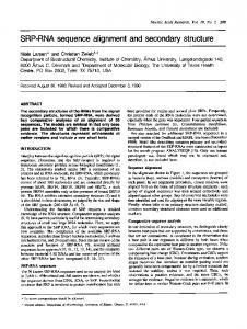
The processor array architecture generalizes the approach taken with the baseline architecture presented in Section 4. The baseline architecture utilizes individual PEs for each computation in the graph-like structure of CMs. This limits the size of the CMs that can be processed using the baseline architecture as the number of PEs is bounded by physical hardware resources. The processor array architecture described in this section employs PEs using a more general technique so that any PE can be utilized to compute the result of any computation in the graph-like structure of a CM. The processor array architecture consists of three main components, an array of processing modules (PMs), a multi-port shared memory structure, and a reporting module. Inputs to the processor array architecture consist of a stream of residues, which is replicated and sent to each PM, and a stream of instructions, which is divided up so instructions are sent to the appropriate PM. The mapping of instructions to PMs is discussed in Section 6.2.2. The architecture outputs only the scores for high scoring alignments. A high-level block diagram of the processor array architecture is illustrated in Figure 11. Each of the main components for the processor array architecture is described in more detail in the following sections.
Reporting Module Processor Array Processing Module 0
Residue Input
PE0_score
Output Scores
Shared Data Memory
PE0_waddr PE0_data[0-5] PE0_raddr[0-5]
Instruction Input
Main Instr. FIFO
Processing Module 1
out[0-5] in[0-5]
PE1_score PE1_waddr PE1_data[0-5] PE1_raddr[0-5]
out[6-11] in[6-11]
Processing Module n
Fig. 11: A high-level block diagram of processor array architecture with two processing modules. The number of processing modules can be scaled as shown with dashed lines. ACM Transactions on Computational Logic, Vol. V, No. N, December 2008.
20
5.2
·
James Moscola et al.
Processing Modules
The processing module is where all of the computation required for the RNA alignment takes place. A block diagram of a PM is shown in Figure 12. The core of the PM is similar to the PEs used in the baseline architecture. Each PE consists of seven saturating adders and five comparators. The first six saturating adders are used to sum results from previous computations with transition probabilities associated with the state of the current computation. The five comparators in the PE determine the maximum value from those summations and pass that value to the final adder in the PE. The final saturating adder adds an emission probability which is selected from the local emission probability memory. When a computation does not require the addition of an emission probability, like those for start (S), delete (D), and bifurcation (B) states, a value of zero is presented to the adder so as not to affect the result of the maximization portion of the PE. Likewise, not all states in a CM have six children states, thus not all computations require all six adders in the maximization portion of the circuit. In such cases, the largest negative number possible (dependent on the number of bits used in the architecture) is presented to the unused adders so as not to affect the result of the maximization portion of the PE.
Processing Module 0 Processing Element: PE0 PE0_data0
+
PE0_data1
+
PE0_data2
+
= Residue Input
=
Instruction Input
= PE0_data3
PE0_data4
PE0 Residue Memory
PE0 Instr. FIFO
PE0_score
+
Reporting Module
+ =
PE0_data5
Local T. Registers
Data read delay
=
+
+
Local E. Registers
write addr. delay
PE0 Covariance Model Memory Data Address Decoder
PE0_waddr PE0_raddr0 PE0_raddr1 PE0_raddr2 PE0_raddr3 PE0_raddr4 PE0_raddr5
Fig. 12: Block diagram of a single PM. Dashed lines represent components that are only needed on the first PM.
In addition to the PE core, PMs also contain a variety of memories for different functions of the PM. An instruction FIFO collects and stores instructions from an input stream until they are ready to be executed. A dual ported residue memory stores a single window’s (W ) worth of residues. Only one port is used when executing computations for the single emission states M L and M R. Both ports are required when executing computations for the pairwise emission state M P . Each PM also contains its own memory for storing CM information such as transition and emission probabilities. Transition and emission probabilities are loaded ACM Transactions on Computational Logic, Vol. V, No. N, December 2008.
Hardware-Accelerated RNA Secondary-Structure Alignment
·
21
into the memory during initialization and reused throughout the computation. Because each PM has its own CM memory, it has unrestricted access to the probabilities required for the alignment computation. Additionally, the CM memory for each PM stores only the probabilities required by the computations that are to be executed on that PM. During an alignment computation, the necessary transition and emission probabilities are read from the CM memory and stored in local registers where they are immediately available to the PE. This design makes effective use of distributed memories, such as block RAMs on an FPGA or embedded SRAM on an ASIC. Data computed by each PM is stored in a shared memory that is shared by all PMs in the processor array architecture. For each instruction executed, each PM may issue up to six reads to the shared memory. The data returned from the shared memory is used as input to the PE adders. Because each PM only produces a single result for each instruction executed, only a single write interface to the shared memory is required. Scaling the performance of the processor array architecture can be accomplished by increasing the number of PMs in the array. A discussion on the scalability of the processor array architecture is presented later in Section 7.4. 5.2.1 Instruction Format. The instruction format utilized by the processor array architecture is a long instruction word that contains all of the information necessary to complete the computation. The instruction format has fields for the state value v, the starting position of a test alignment i, the end position of a test alignment j, six read address pointers raddr0 through raddr5 , and a write address pointer waddr where the result is to be written. An example of the long instruction word is shown below: [v, i, j, raddr0 , raddr1 , raddr2 , raddr3 , raddr4 , raddr5 , waddr] The number of bits required for each of the fields in the instruction word is dependent on a number of factors. The values for v, i, and j must be large enough to handle the largest CMs that are to be processed. Using 10 bits for each of v, i, and j allows the processor array architecture to process CMs with up to 1024 states and window sizes W up to 1024. The number of bits required for each of the read address pointers and the write address pointer is dependent on the number of processors in the processor array architecture. More details on the number of bits required for each pointer are discussed in Section 7.4.2. The analysis presented later in Section 7 is based on fixed-length instructions as described above. However, it would also be possible to use variable-length instructions for the processor array architecture. Based on an analysis of the CMs in the Rfam 8.0 database, the average number of reads required for a computation is approximately 4, where ∼ 42% of computations required 3 reads and ∼ 40% of computations require 6 reads. Eliminating the unnecessary read addresses from instructions could help to reduce the bandwidth required for instruction execution considerably. ACM Transactions on Computational Logic, Vol. V, No. N, December 2008.
22
·
James Moscola et al.
5.2.2 Executing Instructions. Instruction execution on the processor array architecture works similarly to that of a traditional instruction pipeline, with stages for fetching and decoding instructions, reading and writing data memory, and execution. On each clock cycle a single instruction is read from the instruction FIFO of the PM. The seven memory addresses (one write address, and up to six read addresses) are sent to the data address decoder where they are divided onto the respective read of the shared memory interface. The data address decoder also extracts the write address, that is the shared memory location where the result of the instruction should be stored, and sends it to a delay module. The write address is not needed until the computation has completed. Other portions of the instruction that indicate the state number as well as the i and j residue positions for the computation are also delayed until the data from the shared memory becomes available. The data returning from the shared memory represents computations from the CM states that are children of the current CM state computation being executed. Synchronously with the arrival of data from the shared memory, the necessary transition and emission probabilities are read from the CM memory and stored in local registers. Additionally, one or two residues are read from the residue memory and used to select the emission probability that will be used, if any, by the PE to complete the computation. Upon completion of the computation by the PE, the result is written to shared memory in the location specified by the instruction and previously stored in the delay unit. Computations for state v = 0 are not stored in the shared memory structure. Instead, they are sent to a reporting module for further processing.
5.3
Shared Memory Structure
One of the pivotal components of the processor array architecture is the shared memory structure. Throughout the alignment computation, results computed on one PM may be required by other PMs in the processing array. The shared memory structure provides a means for communicating results between PMs. The shared memory structure is a large memory bank composed of many smaller memories, each with its own read and write interfaces. This approach allows a large number of independent reads and writes per clock cycle and increases the effective bandwidth of the memory interface. The shared memory is partitioned in such a way so that each PM writes results to a designated region of the memory. However, each PM can read any location from any of the available memories in the structure. Furthermore, each PM can issue up to six memory reads per clock cycle. Therefore, if the processor array has multiple PMs, the number of concurrent memory reads on any given clock cycle may be as high as 6p where p is the number of PMs in the processing array. The size and number of each memory required in the shared memory structure is dependent on the CM being processed. However, since each PM can issue up to six simultaneous reads to the shared memory structure, the minimum number of individual memories required for each PM is six. A discussion on the required size of those memories is presented in Section 7.3. ACM Transactions on Computational Logic, Vol. V, No. N, December 2008.
·
Hardware-Accelerated RNA Secondary-Structure Alignment
23
5.3.1 Writing Results to the Shared Memory Structure. As previously mentioned, each PM in the processor array architecture is allocated a portion of the shared memory structure where it writes its results. Additionally, because each PM only needs to write a single result per clock cycle, the write interface of the shared memory structure is considerably simpler than the read interface. Figure 13 illustrates the write interface to one region of the shared memory structure. The region shown is for a single PM and consists of six individual memories. In the example configuration, the value being written is an 18-bit value and the write address is a 15-bit value. The most significant bits are used to select which of the available memories in which to write the data. The remaining bits of the write address are used to address the individual memories.
read_addr
data_out
read_addr
PE0 MEM0
data_out
read_addr
PE0 MEM1
data_out
read_addr
PE0 MEM2
data_out
read_addr
PE0 MEM3
data_out
read_addr
PE0 MEM4
data_out
PE0 MEM5
wr_en
wr_en
wr_en
wr_en
wr_en
wr_en
wr_addr
wr_addr
wr_addr
wr_addr
wr_addr
wr_addr
data_in
data_in
data_in
data_in
data_in
data_in
PE0_we
(14:12)
PE0_waddr PE0_score
(14:0)
(11:0)
(17:0)
Fig. 13: Write interface configuration for a single PM with six individual memories
5.3.2 Reading Data from the Shared Memory Structure. The read interface for the shared memory structure allows any PM in the processor array architecture to read a value from any memory in the structure. To accomplish this, the available memories in the shared memory structure are interfaced to the PMs via a pair of switching fabrics. There are many types of switching fabrics available, each with its own pros and cons. The requirements for the shared memory structure are that the switching fabric be non-blocking and that it be scalable. Non-blocking behavior is desirable so that all memory reads have the same known latency. This ensures that all PMs in the processing array can operate continuously without running the risk of desynchronization with other PMs. As described later, synchronization between PMs is built into the schedules for each PM. Using a switching fabric with blocking behavior (i.e. buffering) could stall a memory read for one PM while allowing another to proceed. This could desynchronize the PMs producing unknown results. The switching fabric must also be scalable so that as more PMs are added to the processing array, more read interfaces can be added to the shared memory structure. Given these requirements, a Banyan switch [Goke and Lipovski 1973] was selected to interface the PMs to the memories in the shared memory structure. Banyan switches are non-blocking and scalable [H. Ahmadi and W. Denzel 1989]. Additionally, Banyan switches can be easily pipelined, allowing for very high-speed designs. However, the Banyan switch does have two restrictions that need to be ACM Transactions on Computational Logic, Vol. V, No. N, December 2008.
24
·
James Moscola et al.
Return Addr. Reg
PE0_raddr0 PE0_raddr1 PE0_raddr2 PE0_raddr3 PE0_raddr4 PE0_raddr5
(19:0)
(19:0)
(19:0)
(19:0)
(19:0)
(19:0)
in0
out0
in0
out0
in1
out1
in1
out1
in2
out2
in2
out2
in3
out3
in3
out3
in4
out4
in4
out4
in5
out5
in5
out5
Input Batcher Switch
(15:0)
(15:4)
read_addr read_addr read_addr read_addr 1K x 18bit read_addr 1K x 18bit read_addr 1K data_out xBRAM 18bit
1K xBRAM 18bit 1K xBRAM 18bit BRAM PE0 BRAM wr_en MEM0 wr_en
data_in
Input Banyan Switch
PE1_raddr1 PE1_raddr2 PE1_raddr3
(19:0)
(19:0)
(19:0)
(19:0)
in6
out6
in6
out6
in7
out7
in7
out7
in8
out8
in8
out8
in9
out9
in9
out9
(17:0)
wr_addr wr_en wr_addr wr_en wr_addr wr_addr wr_en wr_addr wr_addr wr_addr wr_addr wr_addr wr_en wr_addr wr_addr
Return Addr. Reg
PE1_raddr0
(21:18)
(3:0)
(15:0)
(15:4)
1K xBRAM 18bit 1K xBRAM 18bit BRAM PE1 BRAM wr_en MEM0 wr_en
out0
in0
out0
in1
out1
in1
out1
in2
out2
in2
out2
in3
out3
in3
out3
in4
out4
in4
out4
in5
out5
in5
out5
Output Batcher Switch
(17:0)
(17:0)
(17:0)
(17:0)
(17:0)
(17:0)
PE0_data0 PE0_data1 PE0_data2 PE0_data3 PE0_data4 PE0_data5
Output Banyan Switch
(21:18)
(3:0) read_addr read_addr read_addr read_addr 1K x 18bit read_addr 1K x 18bit read_addr 1K data_out xBRAM 18bit
in0
(17:0)
in6
out6
in6
out6
in7
out7
in7
out7
in8
out8
in8
out8
in9
out9
in9
out9
(17:0)
(17:0)
(17:0)
(17:0)
PE1_data0 PE1_data1 PE1_data2 PE1_data3
wr_addr wr_en
PE1_raddr4 PE1_raddr5
(19:0)
(19:0)
in10
out10
in10
out10
in11
out11
in11
out11
wr_en wr_addr wr_addr wr_addr wr_en wr_addr wr_addr wr_addr wr_addr wr_addr wr_en wr_addr wr_addr
in10
out10
in10
out10
in11
out11
in11
out11
(17:0)
(17:0)
PE1_data4 PE1_data5
data_in
Fig. 14: Switched read interface for two PMs, each with six individual memories
considered. The first restriction is that no two inputs to the Banyan switch can be routed to the same output port. This would result in contention not only at the output of the Banyan switch, but also at the memory since each memory only has a single read interface. This type of contention is prevented by ensuring that no two PMs are ever scheduled to read the same memory interface on any given clock cycle. Section 6.2.3 provides more details on removing memory contention from the schedule. The second restriction of the Banyan network is that certain inputs can cause internal collisions [H. Ahmadi and W. Denzel 1989]. An internal collision in the Banyan switch can result in one or more of the inputs being routed to the wrong output port. As shown by Batcher, these types of collisions can be avoided by presorting all inputs to the switch [Batcher 1968]. A Batcher switch, which performs a merge sort on its inputs, can be used to pre-sort memory read prior to sending them through the Banyan switch. On each clock cycle, the Batcher switch can take up to k inputs. Those k inputs are then sorted in ascending order and output on the first k outputs of the Batcher switch. The sorted outputs of the Batcher switch can then pass through the Banyan switch with no collisions. Figure 14 shows the configuration of the Batcher and Banyan switches as well as the individual memories. To perform a read on one of the memory interfaces, a PM combines a 16-bit memory address with a 4-bit return address. The most significant bits of the memory address are used to route the read through the switching fabric to the appropriate memory. The remaining bits of the memory address are used to read the required value from the memory. The 4-bit return address is used to route the newly read data back to the appropriate interface of the PM that issued the read. The memory structure in Figure 14 illustrates the structure required when using two PMs, each with six memories. The number of bits required to route memory reads from PMs to the appropriate memory, and the resulting value back ACM Transactions on Computational Logic, Vol. V, No. N, December 2008.
Hardware-Accelerated RNA Secondary-Structure Alignment
·
25
to the PM, varies with the number and size of individual memories in the shared memory structure and the number of PMs in the processor array. 5.4
Reporting Module
The reporting module is a small component that resides at the output of the first processing module. The function of the reporting module is to compare the scores that are output from the processing module to some threshold value and report any scores that exceed that threshold. Along with the score, the reporting module also reports the starting position i and ending position j of the high-scoring alignment. Since the final scores for an alignment are computed in state v = 0 at the root of the CM, and because of the way computations are assigned to the available processing modules (discussed later in Section 6.2.2), only the first processing module requires a reporting module. 6.
SCHEDULING COMPUTATIONS ON THE PROCESSOR ARRAY
The number of PEs that can be utilized by the processor array architecture is dependent on the implementation platform. Platforms with more hardware resources can accommodate more PEs than platforms with fewer hardware resources. To determine how each of the available PEs are used, a polynomial-time scheduling algorithm is employed to determine the ordering of computations and how those computations are distributed among the available PEs. As shown in Section 4, the DP computation required to align a target sequence to a CM can be thought of as a directed task graph. A survey paper by Kwok and Ahmad provides an in-depth survey of static scheduling algorithms for mapping directed task graphs to multiple processors [Kwok and Ahmad 1999]. In this survey, the authors note that there are only three special cases for which there currently exists optimal, polynomial-time scheduling algorithms. Those cases, as enumerated by Kwok and Ahmad [Kwok and Ahmad 1999], are: (1) scheduling treestructured task graphs with uniform computation costs onto an arbitrary number of processors [Hu 1961], (2) scheduling arbitrary task graphs with uniform computation costs on two processors [Coffman and Graham 1972], and (3) scheduling an interval-ordered task graph [Fishburn 1985] with uniform node weights to an arbitrary number of processors [Srinivas and Patnaik 1994]. By using PEs that have constant computational latency, the problem of scheduling the task graph that represents the DP matrix for RNA alignment fits into the first special case listed above. An algorithm developed by T.C. Hu [Hu 1961] provides an optimal, linear-time scheduling algorithm for such problems, and a good starting point for scheduling the DP matrix computations onto the available PEs. 6.1
Optimal Scheduling of Directed Task Graphs
Hu’s scheduling algorithm [Hu 1961] constructs optimal schedules for tree-structured directed acyclic task graphs where each graph node takes unit computation time. The algorithm works for an arbitrary number of processors and can therefore be used regardless of the number of PEs available on a given platform. The scheduling algorithm runs in linear time in terms of the number of DP matrix cells in a CM that need to be scheduled. ACM Transactions on Computational Logic, Vol. V, No. N, December 2008.
26
·
James Moscola et al.
For the processor array architecture, a schedule is constructed for a single window position of the CM over the input genome database. That schedule can then be reused for each window position of the CM. Hu’s scheduling algorithm processes each cell in the DP matrix as a graph node in a task graph. The first stage of the scheduling algorithm involves labeling each of the nodes in the graph with a distance value. Starting from the exit node of the graph (all S0,j,d cells of ROOT0 are exit nodes and all Ev,j,d cells are entry nodes), each node is labeled with its distance from the exit node. The distance of a node is the number of graph edges between that node and the exit node. If multiple paths exist, a node is assigned the distance of the longest path. Once all the nodes in the graph have been labeled, an optimal schedule for a platform with p processors can be constructed as follows: (1) schedule the p (or fewer) nodes with the greatest distance labels and no predecessors. If there are more than p nodes with no predecessors, nodes with higher distance labels should be scheduled first. If there are fewer than p nodes with no predecessors, then fewer than p nodes must be scheduled and some processors will go unused during that time slot; (2) remove the nodes that were scheduled in step (1) from the graph; (3) repeat steps (1) and (2) until all nodes are scheduled and there are no more nodes in the graph. Figure 15 provides a flow diagram of Hu’s scheduling algorithm. Figure 16(a) illustrates an example task graph where each node is labeled with a distance d from the end node N0. A schedule developed using Hu’s algorithm for an unlimited number of processors (i.e. p = ∞) is shown in Figure 16(b). Figure 16(c) shows a schedule for the same task graph when only two processors are available.
Schedule the p (or fewer) nodes with the greatest distance labels and no predecessors
Label nodes with distance labels
Remove the newly scheduled nodes from the graph
Yes
No Done
More nodes in graph?
Fig. 15: Flow Diagram of Hu’s scheduling algorithm
6.2
Scheduling Task Graphs on Finite Resources with Computational Latency
While Hu’s scheduling algorithm does provide a good starting point for scheduling the DP matrix computations, there are a few shortcomings with Hu’s algorithm as it relates the desired application. The first of these shortcomings is that the algorithm does not account for physical hardware resources or computational latencies. For example, the example schedule in Figure 16(b) shows that graph nodes N2 and N1 can be scheduled at time t = 1, and that the graph node N0 can be scheduled in ACM Transactions on Computational Logic, Vol. V, No. N, December 2008.
Hardware-Accelerated RNA Secondary-Structure Alignment
N5 d=2
N4 d=2
N2 d=1
N3 d=1
N1 d=1
Schedule:
Schedule:
t = 0: N5, N4, N3 t = 1: N2, N1 t = 2: N0
t = 0: t = 1: t = 2: t = 3:
·
27
N5, N4 N3, N2 N1 N0
N0 d=0
(a)
(b)
(c)
Fig. 16: (a) An example task graph with distance labels; (b) schedule for task graph in (a) using unlimited processors; (c) schedule for task graph in (a) using two processors
the subsequent time slot t = 2. However, if the computation represented by node N0 is dependent upon the result of the computation represented by node N1, and there is some latency associated with computing the result of node N1, then node N0 cannot be scheduled until time tN 0 = tN 1 + l, where l is the computational latency. Another hardware restriction that Hu’s scheduling algorithm does not take into account is memory. The problem originates from the arbitrary choice of p computations from the pool of available computations at each time slot. In scheduling computations arbitrarily, Hu’s algorithm does not account for the possibility that multiple computations may require accessing different data from the same memory bank. Without memory arbitration, this could lead to potential memory conflicts. With memory arbitration, additional control would be required to ensure that the PEs do not become desynchronized. Finally, Hu’s algorithm does not take advantage of any problem-specific knowledge. For example, if there are more than p computations that can be scheduled in a particular time slot, each with an identical distance label, Hu’s algorithm does not differentiate between them. Instead, p of the available nodes are chosen arbitrarily and scheduled. Choosing nodes more intelligently by utilizing additional information associated with each node may help to reduce the hardware resources required and the total time required to complete the computation. The remainder of this section describes several modifications that were made to Hu’s scheduling algorithm to produce an algorithm suitable for scheduling the DP matrix computations for RNA alignment onto an array of processors while accounting for hardware restrictions. Instead of specifying some number of processors to Hu’s scheduling algorithm and allowing the algorithm to choose the ordering of computations arbitrarily, Hu’s scheduling algorithm is run on a task graph assuming an unlimited number of processors. The output is an optimal schedule for the task graph that provides the earliest possible time that each node can be scheduled (see Figure 16(b)). From that schedule, restrictions can be introduced and intelligent decisions can be made regarding which of the available computations should be scheduled in a given time slot. A flow diagram of the modifications to Hu’s ACM Transactions on Computational Logic, Vol. V, No. N, December 2008.
28
·
James Moscola et al.
schedule is shown in Figure 17.
Remove computations from time slot at head of Hu’s schedule
Schedule CM with Hu’s algorithm using unlimited processors
Sort computations descending by state and ascending by schedulable time
Assign computations to available processors
Add computational latency to children of all scheduled computations
Resolve memory conflicts
Yes
No Done
More time slots in Hu’s schedule?
Fig. 17: Flow Diagram of Modified Hu’s scheduling algorithm
6.2.1 Accounting for Computational Latency. The first modification to Hu’s scheduling algorithm was developed to account for the computational latency of the PEs used in the architecture. Although the time to complete each computation is uniform, this time must still be represented in the schedule. This is because each time slot in the schedule is the equivalent of a single clock cycle in hardware, and without the appropriate delays built into the schedule a computation may be scheduled to execute prior to the availability of a required result from a previous computation. Accounting for the latency of a computation can be done by recursively traversing the task graph and setting the scheduled time for each child of a node n to tchildN ode = max(tchildN ode , tn + l). Figure 18(b) shows the effect of adding computational latency equal to 10 time units into the schedule. Note that the scheduled times for the nodes in Figure 18(b) are no longer t = 0, 1 and 2 as they were in Hu’s original algorithm (Figure 15), but instead t = 0, 10 and 20.
N5 d=2
N4 d=2
N2 d=1
N3 d=1
N1 d=1
Schedule:
Schedule:
t = 0: N5, N4, N3 t = 10: N2, N1 t = 20: N0
t = 0: t = 1: t = 10: t = 20:
N5, N4 N3 N2, N1 N0
N0 d=0
(a)
(b)
(c)
Fig. 18: (a) An example task graph with distance labels; (b) schedule for task graph in (a) using unlimited processors and accounting for a 10 time unit computational latency; (c) schedule for task graph in (a) using two processors and accounting for a 10 time unit computational latency ACM Transactions on Computational Logic, Vol. V, No. N, December 2008.
Hardware-Accelerated RNA Secondary-Structure Alignment
·
29
Accounting for computational latency in the initial Hu schedule will still result in an optimal schedule with regards to how quickly the hardware platform can correctly produce the result of the desired computations. If no other changes are made to the initial Hu schedule, then a modified Hu schedule that accounts for the computational latency of the hardware will be exactly ScheduleLengthHu × l in length. However, throughout the development of a schedule, computations may be delayed for various other reasons as described in the next few sections. Each time the scheduled time of a computation is adjusted for other conflicts, all descendants of that computation in the task graph need to be adjusted to account for the computational latency. Because not all conflicts are resolved optimally, the final modified schedule may no longer be optimal. 6.2.2 Processor Assignment. The schedule produced in the previous section accounts for the computational latency. However, it still assumes that there are an infinite number of processors on which to schedule the computation. From the assumption of an unlimited number of processors, a schedule can be obtained for a given CM that completes the work as quickly as possible. A bound on the number of useful processors can then be obtained from that schedule, assuming every computation is completed on a different processor. While a finite number of processors now suffices, instantiation of so many processors (see Section 4.4) will likely exceed any reasonable resource availability. Thus, we must consider the issues that arise from scheduling a CM to execute on a number of processors that is relatively small compared to the maximum number of processors that could be used. Thus, the next modification to the schedule accounts for the limited number of processors, or PEs, available in the architecture. Starting with the schedule produced in Figure 18(b), if the number of processors available is limited to two processors, the schedule must be altered to reduce the number of computations at time t = 0. All three computations represented by nodes N5, N4, and N3 cannot be computed in the same time slot. Instead, one of those computations must be delayed and scheduled at a later time. In the example shown in Figure 18(c), the computation for node N3 is delayed one time unit and rescheduled at time t = 1. Node N3 is not dependent on nodes N5 or N4, so it is not necessary to delay node N3 more than a single time unit. Node N0, which is dependent on node N3, is unaffected by N3’s newly scheduled time because it is scheduled for time t = 20 which is greater than tN 3 + l where l is still 10 time units. Because this adjustment is dependent on the actual number of PEs available, as the architecture is scaled to include more PEs, new schedules will need to be generated. In the above example, the computation for node N3 was arbitrarily chosen to be delayed while nodes N5 and N4 remained scheduled at time t = 0. However, when scheduling the DP matrix computations for aligning an RNA sequence to a CM, the choice of which computations should be assigned to which PEs, and which computations should be delayed, is based on a number of factors. The first factor in determining the ordering and processor assignment of computations is based on how CM information, such as transition and emission probabilities for each CM state, is stored by the processor array architecture. If all of the CM information were to be stored in a single memory in the processor array architecture, then PEs could not efficiently retrieve the probabilities required ACM Transactions on Computational Logic, Vol. V, No. N, December 2008.
30
·
James Moscola et al.
if computations for multiple different CM states were scheduled in a single time slot. This is because different CM states require different transition and emission probabilities and scheduling multiple different states in a single time slot would result in memory contention. Instead, all computations for a particular CM state are assigned to the same PE regardless of where they occur in the schedule. This allows the CM information to be divided among several smaller memories that are local to each PE. Each PE stores only the portion of the CM information that is required for the states that it is scheduled to process. This eliminates any contention that may have occurred by storing CM information in a global memory used by all PEs. Computations are assigned to a PE based on their CM state number, P E# = v % p, where v is the CM state number to which the computation is a member, and p is the number of PEs available. Other information about the computations is also used to determine the order in which computations should be completed and which computations are delayed. As shown in Figure 4, the DP parsing algorithm treats CMs as a tree structure and computes values starting at the bottom of the tree and ending at the top of the tree. That is, the algorithm computes values from state v = M − 1 down to v = 0. Computations in each time slot are scheduled in a similar fashion, where those with higher state values are scheduled first. If there are multiple computations with the same state value in a given time slot, then those with the earliest schedulable time are scheduled first. Note that the earliest schedulable time may not be the actual time that a computation is scheduled due to the limited hardware resources. As an example, refer back to Figures 18(b) and (c) where the earliest schedulable time for node N3 was t = 0, but the actual time the node was scheduled was t = 1. 6.2.3 Eliminating Memory Contention. The last consideration when developing a schedule for the processor array architecture is memory contention. As described in Section 5.3.2, no two computations can access the same memory interfaces in any given time slot of the schedule. To prevent memory conflicts, computations are first assigned to processors as described in the previous sections. Then, for each instruction in a time slot, unique memory addresses are provided from which to read previous results in the alignment computation. Each address assigned is bounded to the region of memory that is associated with the computation that produced the result. This, in turn, assigns write locations to the computations that generated the results. In general, more than one computation in the alignment may require the same result from a previous computation. When scheduled in different time slots, there is no conflict since each of the computations can access the result from memory uncontested during its time slot. However, in some circumstance two computations may require the same result in the same time slot. When this occurs, one of the computations needs to be moved to a different time slot. The example shown in Figure 19(b) illustrates a schedule with a time conflict at time t = 10 where both node N2 and N1 need the result of node N4. Because both computations cannot access the same memory in the same time slot, node N1 is moved to the next time slot t = 11. While this technique may not produce an optimal scheduling of the computations, it is likely that an optimal approach is NP-complete. ACM Transactions on Computational Logic, Vol. V, No. N, December 2008.
·
Hardware-Accelerated RNA Secondary-Structure Alignment
N5 d=2
N4 d=2
N2 d=1
N3 d=1
N1 d=1
Schedule:
Schedule:
t = 0: t = 1: t = 10: t = 20:
t = 0: t = 1: t = 10: t = 11: t = 21:
N5, N4 N3 N2, N1 N0
31
N5, N4 N3 N2 N1 N0
N0 d=0
(a)
(b)
(c)
Fig. 19: (a) An example task graph with distance labels; (b) schedule for task graph as shown in Figure 18, but with a memory conflict at time t = 10; (c) schedule for task graph with memory conflict resolved. Note that N1 was moved to t = 11 and its dependent N0 was moved to tN 0 = tN 1 + l = 21.
7.
ANALYSIS OF THE PROCESSOR ARRAY ARCHITECTURE
This section provides an analysis of the processor array architecture and the proposed scheduling technique. From more than 600 CMs in the Rfam database, four were selected to illustrate the behavior of the processor array architecture and the scheduler. The four CMs chosen are of average size with varying numbers of bifurcation states. The characteristics of the four models (RF00001, RF00016, RF00034, RF00041) are shown in Table IV. Data and analysis for additional for additional models can be found in [Moscola 2008]. CM
Num Nodes
Num States
W
Num ROOT
Num MATP
Num MATL
Num MATR
Num BIF
Num BEGL
Num BEGR
Num END
RF00001
91
366
137
1
34
31
20
1
1
1
2
RF00016
107
352
176
1
11
59
35
0
0
0
1
RF00034
104
343
131
1
18
61
11
3
3
3
4
RF00041
102
377
146
1
29
61
2
2
2
2
3
Table IV: Covariance Model Data
7.1
Running Time
The first thing to consider when analyzing the effectiveness of the scheduler is the running time, or the length of the schedule required to produce results. The schedules for the processor array architecture are developed for a single window W of the DP computation. The schedule length, in clock cycles, for a single window of four different CMs is shown in Figure 20. As should be expected, as the number of processors in the processor array increases, the length of the schedule decreases. This is because the total number of computations in the DP matrix stays the same regardless of the number of processors. However, with more processors available, more computations can be done in parallel which decreases the time required for the computation. The most dramatic decreases in schedule length occur between ACM Transactions on Computational Logic, Vol. V, No. N, December 2008.
·
32
James Moscola et al.
one and sixteen processors. The number of bifurcation states in a model does not appear to have an affect on the decreasing schedule length.
Schedule Length (Cycles)
1.E+07
1.E+06
1.E+05
1.E+04 1
2
4
8
10
16
32
64
100
128
256
1000
Number of Processors RF00001
RF00016
RF00034
RF00041
Fig. 20: The length of the scheduled computation decreases as the number of processors available for the computation increases (shown on a log-log scale).
7.2
Scheduling Efficiency
Section 7.1 illustrated that as the number of processors in the processor array increases, the length of the scheduled computation decreases. Although adding more processors consistently decreases the schedule length, it is far from linear. As more processors are added, there are diminishing decreases in the schedule length. This can be illustrated as the speedup and efficiency of a schedule as more processors are added. The speedup is a measure of how much faster a computation can be done with p processors than with a single processor. The speedup is measured as ScheduleLength1 proc ScheduleLengthp procs . The efficiency of the schedule is a measure of how much idle time must be inserted into the schedule to ensure no conflicts during the computation. This is measured as N umComputations where N umCompuations is the number T otalCycles of computations that need to completed for a single window of the specified CM and T otalCycles is the total number of clock cycles, among all processors, that are required to compute the results, including any idle time in the schedule. Figure 21 illustrates both the speedup and the schedule efficiency of the four example CMs. As additional processors are added to the processor array the speedup increases. However, there are diminishing returns as the schedule is divided over more processors. This is especially true for models RF00001, RF00034, ACM Transactions on Computational Logic, Vol. V, No. N, December 2008.
·
Hardware-Accelerated RNA Secondary-Structure Alignment
140
33
100% 90% 80%
100
70% 60%
80
50% 60
40%
Schedule Efficiency (%)
Speedup Over Single Processor
120
30%
40
20% 20 10% 0
0% 0
50
100
150
200
250
Number of Processors RF00001
RF00016
RF00034
RF00041
(speedup)
RF00001
RF00016
RF00034
RF00041
(efficiency)
Fig. 21: The speedup shows the diminishing returns as more processors are added to the processors array. The efficiency decreases as more processors are added to the processors array, indicating that more idle time is inserted into the schedule as the number of processors increases.
and RF00041, which have 1, 3, and 2 bifurcations states respectively. CM RF00016 has no bifurcation nodes and shows much greater speedup with the addition of more processors. This behavior is likely due to the combination of the way computations are assigned to processors (P E# = v % p) and the fact that bifurcation states require a much larger number of computations than non-bifurcation states. These two factors result in a much larger number of computations, those for the bifurcation states, being assigned a single processor. This, in turn, could result in a large number of idle slots being inserted into the schedules for each of the other processors to ensure that all schedules remain synchronized. However, it was noted in Section 6.2.2 that computations are assigned to processors in such a way so as to eliminate the need to unnecessarily duplicate CM transition and emission probabilities. Because bifurcation states do not require probabilities other than those from its children states, it may be possible to evenly distribute bifurcation computations over all available processors in the processor array. This could allow CMs with bifurcations nodes to achieve speedup similar to that of CMs without bifurcation nodes. 7.3
Memory Requirements
One of the main challenges in considering an architecture to accelerate the RNA alignment computations was determining how to handle the memory requirements of the computations. This section provides an analysis on the memory requirements and behaviors for the processor array architecture and the scheduler. ACM Transactions on Computational Logic, Vol. V, No. N, December 2008.
·
34
James Moscola et al.
7.3.1 Live Memory Requirements. Figure 22 illustrates the maximum amount of live memory required for a schedule as the number of processors increases. The live memory is the number of DP matrix cells that need to be stored throughout the computation because another computation is still dependent on the value from that cell. Once a stored value no longer has any dependencies, its memory location can be reclaimed. 120,000
Max Live Memory (Cells)
100,000
80,000
60,000
40,000
20,000
0 0
50
100
150
200
250
Number of Processors RF00001
RF00016
RF00034
RF00041
Fig. 22: The maximum amount of live memory remains fairly consistent regardless of the number of processors.
Increasing the number of processors has very little affect on the maximum amount of live memory required throughout an alignment computation. This means that the total memory required for processor array architecture is independent of the number of processors in the array. 7.3.2 Average Memory/Processor. Figure 22 illustrates the maximum amount of live memory required for a computation for the complete array of processors. However, as discussed in Section 5.3 each processor in the processor array architecture has its own memory in the shared memory structure to which it can write data. Figure 23 illustrates the average memory required per processor as the number of processors increases. When using a single processor, all of the memory required must be associated with that one processor. This can be verified by noting that the average memory required for a single processor, as shown in Figure 23, is equivalent to the maximum live memory required for a single processor in Figure 22. Figure 22 also shows that as the number of processors in the processor array increases, and hence the total number of individual memories, the amount of memACM Transactions on Computational Logic, Vol. V, No. N, December 2008.
·
Hardware-Accelerated RNA Secondary-Structure Alignment
35
120,000
Average Memory/Processor (Cells)
100,000
80,000
60,000
40,000
20,000
0 0
5
10
15
20
25
30
Number of Processors RF00001
RF00016
RF00034
RF00041
Fig. 23: As the number of processors in the processor array architecture increases, the average memory required per processor decreases.
ory required for each processor decreases. This is because the total number of DP matrix cells that need to be stored does not vary much as the number of processors increases, thus the same number of cells are being stored over a larger number of memories. The decrease in efficiency shown in Figure 21 does not affect the number of cells that need to be stored throughout the computation. 7.3.3 Memory Traces. To understand the behavior of the memory usage throughout an RNA alignment computation, several computations were simulated for two different CMs from the Rfam database. Memory traces were created for the duration of the simulated computation to monitor the required memory throughout the computation. The models chosen to illustrate memory usage were RF00016 and RF00034, which have 0 and 3 bifurcation states respectively. Each of the models were run three times each to simulate 16, 32, and 64 processor configurations. The memory traces for CM RF00016 are shown in Figure 24. The memory traces for CM RF00034 are shown in Figure 25. The overall profile of each memory trace is a result of the structure of the CM. Therefore, the memory traces for the two CMs have very distinct curves. However, comparing the traces for the two CMs helps to reveal some commonalities in the behavior of the memory usage. First, note that the profile of the memory traces remain fairly consistent regardless of the number of processors. The time scale of the profile is simply compressed or expanded depending on whether there are more or fewer processors. Also note that the peak of each profile (i.e. the maximum live memory) is approximately equivalent regardless of the number of processors. ACM Transactions on Computational Logic, Vol. V, No. N, December 2008.
36
·
James Moscola et al.
70,000 16 procs 32 procs 64 procs
Live Memory (Cells)
60,000
50,000
40,000
30,000
20,000
10,000
0 0
50,000
100,000
150,000
200,000
250,000
300,000
350,000
400,000
Time Slot Fig. 24: Memory trace for CM RF00016
100,000 16 procs 32 procs 64 procs
90,000
Live Memory (Cells)
80,000 70,000 60,000 50,000 40,000 30,000 20,000 10,000 0 0
50,000
100,000
150,000
200,000
250,000
300,000
Time Slot Fig. 25: Memory trace for CM RF00034
ACM Transactions on Computational Logic, Vol. V, No. N, December 2008.
350,000
400,000
Hardware-Accelerated RNA Secondary-Structure Alignment
·
37
This means that the total memory required for the processor array architecture is independent of the number of processors in the array. This was also shown earlier in Figure 22. 7.4
Scalability of Architecture
This section provides an analysis on the scalability of the processor array architecture. It includes a discussion on the logic requirements and the I/O requirements. 7.4.1 Logic Requirements. To determine the logic requirements for different sized processor array architectures, the main components were scaled according to the number of processors in the array. For the processing elements discussed in Section 5.2, this entailed finding the resource requirements for a single processing element and then multiplying those requirements by the number of processors desired. For the shared memory structure, scaling the resource requirements entailed not only increasing the number of ports on the switching fabrics, but also increasing the width of each port. The increased width of each port is due to the additional bits required to address the larger number of ports. Note that the number of processors chosen was determined by the number of ports available on the switches of the shared memory structure. The switches scale as a power of two and the number of processors was chosen to use those � as many of � ports as possible. orts The number of processors chosen is simply N umSwitchP . The results of the 6 scalability analysis can be seen in Table V. Processor Array Configuration Num Procs
1
2
5
10
21
42
85
170
341
Num Memories
6
12
30
60
126
252
510
1020
2046
Switch Ports
8
16
32
64
128
256
512
1024
2048
Port Address Bits
3
4
5
6
7
8
9
10
11
In Switch Port Size
16
18
20
22
24
26
28
30
32
Out Switch Port Size
21
22
23
24
25
26
27
28
29
180048 (2%)
Resource Requirements in LUTs Processing Elements
528 (15%)
1056 (10%)
2640 (8%)
5280 (6%)
11088 (5%)
22176 (4%)
44880 (3%)
89760 (2%)
Banyan Switch (in)
396 (11%)
1186 (11%)
3286 (10%)
4344 (5%)
6364 (3%)
10404 (2%)
18515 (1%)
34562 (1%)
66913 (1%)
Batcher Switch (in)
889 (26%)
3286 (30%)
11292 (33%)
35005 (40%)
102323 (44%)
285696 (47%)
762749 (48%)
1994099 (49%)
5098195 (50%)
Banyan Switch (out)
517 (15%)
1442 (13%)
3767 (11%)
4729 (5%)
6620 (3%)
10404 (2%)
17874 (1%)
32639 (1%)
62453 (1%)
Batcher Switch (out)
1130 (33%)
3927 (36%)
12735 (38%)
37699 (43%)
105914 (46%)
285696 (47%)
744706 (47%)
1899186 (47%)
4747949 (47%)
Total Size
3460
10897
33720
87057
232309
614376
1588725
4050246
10155559
3954918
Resource Requirements in Gates Processing Elements
11598
23196
57990
115980
243558
487116
985830
1971660
Banyan Switch (in)
5451
16335
45319
59859
87339
142299
254453
472481
913541
Batcher Switch(in)
11937
44279
149115
469425
1368370
3782106
10168566
26570852
67901931
Banyan Switch (out)
7137
19919
52045
65241
90923
142299
245487
448320
858036
Batcher Switch (out)
15303
53245
169293
507093
1418588
3799730
9917324
25246972
63014048
Total Size
51426
156974
473762
1217598
3208778
8353550
21571660
54710285
136642474
Table V: Configuration and resource requirements for different sized processor arrays.
In terms of the individual memories required, if each processor in the processor array architecture is given six memories as described in Section 5.3, then the total number of individual memories required is 6p where p is the number of processors. One of the largest FPGAs available today, the Xilinx Virtex-5, contains over 600 1024x18bit block RAMs, allowing for a total of over 600,000 18-bit memory locations (or 300,000 21-bit memory locations if using the numeric representation discussed in Section 3.5). As shown in Section 7.3, the live memory requirements ACM Transactions on Computational Logic, Vol. V, No. N, December 2008.
·
38
James Moscola et al.
(i.e. the number of memory locations required) rarely exceeds 100,000 entries for the CMs tested. Furthermore, as the number of processors is increased, the average memory required per processor decreases. Because the maximum amount of live memory stays fairly consistent regardless of the number of processors (22), the average memory required per processor has an almost perfect inverse relationship to the number of processors. That is, doubling the number of processors reduces the average memory required per processor by half. However, because the memory requirements differ for each CM, no general statement can be made regarding the ability, or the inability, of a hardware device to handle all CMs. Each CM must be considered individually with respect to the resources available. To determine if a device can support m number of processors, the following l a CM using a specified AverageM emP erP roc must be true: p × 6×N umEntriesP erBRAM ≤ N umBRAM sAvailable. 1.60E+08
200,120 180,120
1.40E+08
160,120
Number of LUTs
1.00E+08
120,120 100,120
8.00E+07
80,120
6.00E+07
Number of Gates
1.20E+08 1401,20
60,120 4.00E+07 40,120 2.00E+07
20,120 120
0.00E+00 0
50
100
150
200
250
300
350
Number of Processors Processing Elements
Banyan Switches
Fig. 26: Resource requirements for the processing elements and Banyan switches in different sized processor arrays.
The logic requirements for the processor array architecture, in terms of both look-up tables (LUTs) and the equivalent gate count, are shown in Table V and illustrated in Figures 26 and 27. While the resource requirements for the processing elements and the Banyan switch scale linearly, the Batcher switch does not. Moreover, as shown in Figure 27 the logic requirements for the Batcher switch quickly dwarf the logic requirements for other key components of the architecture. Note that the logic requirements for the Batcher switch closely follow the total logic requirements of the complete architecture. When using a single processor in ACM Transactions on Computational Logic, Vol. V, No. N, December 2008.
Hardware-Accelerated RNA Secondary-Structure Alignment
·
39
1.60E+08
12,000,120
1.40E+08 10,000,120
1.00E+08
8.00E+07
6,000,120
6.00E+07
Number of Gates
Number of LUTs
1.20E+08 8,000,120
4,000,120 4.00E+07 2,000,120 2.00E+07
120
0.00E+00 0
50
100
150
200
250
300
350
Number of Processors Total
Processing Elements
Banyan Switches
Batcher Switches
Fig. 27: Resource requirements for different sized processor arrays. Note that the Batcher switches account for the majority of the resources.
the processor array, the Batcher switch accounts for almost 60% of the logic resources. This quickly grows to about 90% of the total resources when using only 21 processors. Given the rapid growth of the Batcher switch, the logic requirements quickly become the limiting factor in terms of the number of processors that can be deployed on today’s devices. Even though the Xilinx Virtex-5 has enough block RAMs to support up to 100 processors, with only 200K LUTs, the device is limited to fewer than 20 processors. However, with ASIC devices currently supporting over 1.5 billion transistors [Shiveley 2006], 340 or more processors on an ASIC is possible. 7.4.2 I/O Requirements. This section examines the I/O requirements of the processor array architecture. There are three components to the I/O: the score output, the residue input, and the instruction input. As described in Section 5.4, only a single processing element (PE0) outputs alignment scores. Furthermore, scores are only output for state v = 0, meaning that the number of potential scores that need to be output consists of only a small fraction of the overall computation. Because only scores that exceed some predetermined threshold are output, the number of scores output will generally be much less than the total number of scores in state v = 0. For the CMs in Table IV, as well as many others from the RFAM database, the size of the output scores for a single window W is typically less than a few hundred KBytes. This translates to an average required output bandwidth of approximately 5 MBps for a single processor configuration and approximately 400 MBps for a 256 processor configuration when ACM Transactions on Computational Logic, Vol. V, No. N, December 2008.
40
·
James Moscola et al. Processor Array Configuration
Num Procs
1
2
5
10
21
42
85
170
341
Num Memories
6
12
30
60
126
252
510
1020
2046 2048
Switch Ports
8
16
32
64
128
256
512
1024
Port Address Bits
3
4
5
6
7
8
9
10
11
In Switch Port Size
16
18
20
22
24
26
28
30
32
Out Switch Port Size
21
22
23
24
25
26
27
28
29
Instruction I/O Requirements @ 250 MHz Instruction Size
121
127
133
139
145
151
157
163
169
I/O Requirements (bits)
121
254
665
1390
3045
6342
13345
27710
57629
I/O Requirements (Gbps)
30.25
63.5
166.25
347.5
761.25
1585.5
3336.25
6927.5
14407.25
Table VI: The instruction sizes and bandwidth required for streaming instructions to the processor array architecture.
running the processor array architecture at 250 MHz. The residue input consists of a single new residue for each window W of the computation. Because each residue can be represented with only a few bits of information, and each window may contain millions of instructions, the residue input is insignificant when compared to the instruction input. When running the processor array architecture at 250 MHz, the bandwidth required for the residue input is on average less than 1 KByte for a single processor configuration and approximately 5 KBytes for a 256 processor configuration. The instruction input is the main component of the I/O and is the limiting factor for processor array architecture. The instruction input consists of a stream of instructions for each processor in the processor array that identifies the computations for each processor. As the number of processors increases, the number of instructions that must be streamed to the processor array architecture also increases. Additionally, increasing the number of processors also increases the size of each instruction that must be streamed to the architecture. As described in Section 5.2.1, each instruction consists of up to six memory addresses from which to read memory and a single memory address to which the result should be written. As the number of processors increases, the number of address bits required to access each of the individual memories in the shared memory structure also increases. Table VI shows the instruction sizes required for different configurations of the processor array architecture. Also shown in Table VI is the number of instruction bits per clock cycle that must be provided to the processor array to fully utilize all of the available processors. This value can be used to determine the required input bandwidth for streaming instructions to the processor array architecture. The bandwidth requirements shown in Table VI are for a processor array architecture running at 250 MHz. At first glance the bandwidth required for streaming instructions to the processor array seem a bit daunting. However, the actual schedules tend to be only several hundreds of MBytes in size. When divided over a couple of processors, the size of the schedule assigned to each processor is typically around 50 MBytes. When using a large number of processors in the processor array, the size of the schedule assigned to each processor can be less than 1 MByte. Furthermore, the same schedule is reused for each window of the computation. Therefore, providing each processor in ACM Transactions on Computational Logic, Vol. V, No. N, December 2008.
Hardware-Accelerated RNA Secondary-Structure Alignment
·
41
the processor array architecture with a small SRAM or DRAM for schedule storage could provide the bandwidth necessary to keep all of the processors in the processor array architecture busy. 7.5
Comparison to Infernal Software
To determine the effectiveness of the processor array architecture, this section compares its estimated runtime to that of the Infernal software package. While some results are presented in this paper, additional results can be found in [Moscola 2008]. The evaluation system for the Infernal software contains dual Intel Xeon 2.8 GHz CPUs and 6 GBytes of DDR2 SDRAM running Linux CentOS 5.0. Infernal was run with the –toponly and –noalign options to ensure that Infernal was not doing more work than the processor array architecture. Results were collected for both the standard version of Infernal as well as Infernal using the Query Dependent Banding (QDB) heuristic [Nawrocki and Eddy 2007]. The runtime represents the time it took, in seconds, for Infernal to process a randomly generated database of 1 million residues. The database search algorithm that is executed by Infernal is equivalent to the algorithm presented in Section 3.3 which does not require a traceback algorithm. Since no traceback is required, the contents of the residue database have no affect on the runtime. The results for the processor array architecture are an estimate based on several factors including: the number of computations required to process a database of 1 million residues, the efficiency of the schedule, the number of processors available, and the clock frequency of the processor array. For the estimates in this section, a clock frequency of 250 MHz was used. Table VII shows the results for four different CMs using 16, 32, and 64 processors. In the table, Total Computations represents the total number of computations required to compute the results for a database of 1 million residues. This value includes all of the computations, including the expanded computations required for scheduling the DP matrix cells from bifurcation states. The efficiency value was Time (seconds)
Infernal Time (seconds)
Infernal Time (QDB) (seconds)
Speedup over Infernal
Speedup over Infernal (w/QDB)
CM
Total Computations
Efficiency
Total Cycles
Schedule Length
RF00001
52178338429
71.4
73072036714
4567002295
18.27
3494.92
1284.43
191.31
70.31
RF00016
62121487523
95.74
64884170889
4055260681
16.22
3360.00
1885.21
207.14
116.22
16 Processors
RF00034
50108566254
53.09
94373229739
5898326859
23.59
3148.36
875.20
133.44
37.10
RF00041
59389512497
66.69
89048404795
5565525300
22.26
3881.56
1186.92
174.36
53.32
RF00001
52178338429
53.75
97071025316
3033469541
12.13
3494.92
1284.43
288.03
105.85
RF00016
62121487523
91.44
67929980421
2122811888
8.49
3360.00
1885.21
395.70
222.02
RF00034
50108566254
40.92
122439740504
3826241891
15.30
3148.36
875.20
205.71
57.18
RF00041
59389512497
49.1
120945137629
3779535551
15.12
3881.56
1186.92
256.75
78.51
RF00001
52178338429
36.85
141581036608
2212203697
8.85
3494.92
1284.43
394.96
145.15
RF00016
62121487523
82.66
75149663664
1174213495
4.70
3360.00
1885.21
715.37
401.38
RF00034
50108566254
25.17
199009881845
3109529404
12.44
3148.36
875.20
253.12
70.36
RF00041
59389512497
32.05
185255436066
2894616189
11.58
3881.56
1186.92
335.24
102.51
32 Processors
64 Processors
Table VII: Estimated runtime and speedup of processor array architecture over Infernal software package. Estimate is based on a processor array running at 250 MHz. ACM Transactions on Computational Logic, Vol. V, No. N, December 2008.
42
·
James Moscola et al.
determined in Section 7.2 for a single window of the alignment computation. The total number of cycles required for processing 1 million residues, including idle time, . Because those cycles are divided evenly across p is estimated as T otalComputations Ef f iciency processors, the actual length of the schedule is T otalCycles . The time to process the p schedule varies with the frequency at which the processor array architecture can process the schedule. For the comparison presented in this section, the frequency of the processor array architecture is assumed to be 250 MHz. The times listed in Table VII for the processor array architecture are computed as ScheduleLength . For 250M Hz comparison the table lists the time required for both the standard Infernal software package and the Infernal software package when using the QDB heuristic. The speedup represents the speedup of the processor array architecture over the Infernal software package. Figure 28 illustrates the estimated time to align 1 million residues to a CM when using between 1 and 256 processors in the processor array. Results for four different CMs are shown. The shortest bars represent the time required when using 256 processors. The longest bar represents the time required when using a single processor. The bars in between represent the time required when using 128, 64, 32, 16, 8, 4, and 2 processors.
RF00001 - ProcArray
RF00016 - ProcArray
RF00034 - ProcArray
RF00041 - ProcArray
0
50
100
150
200
250
Time (seconds)
Fig. 28: The estimated time to align a 1 million residue database to four different CMs using varying numbers of processors. The shortest bar represents the time to compute the results using 256 processors. The longest bar represents the time to compute the results using a single processor.
Figure 29 compares the estimated time for the processor array architecture to the time for the Infernal software package. The bars showing the results for the processor array architecture are the same as those shown in Figure 28 but on an expanded time scale. The bars showing the results of the Infernal software package contain the results for both the standard Infernal software and the Infernal software when using the QDB heuristic. The shorter bar represents the results when using the QDB heuristic. The longer bar represents the results when using the standard Infernal software. Based on the results in this section, when running at 250 MHz the processor array architecture can achieve an estimated speedup of 11× to 18× over the standard Infernal software package. With 64 processors, the processor array architecture ACM Transactions on Computational Logic, Vol. V, No. N, December 2008.
Hardware-Accelerated RNA Secondary-Structure Alignment
·
43
RF00001 - ProcArray RF00001 - Infernal
RF00016 - ProcArray RF00016 - Infernal
RF00034 - ProcArray RF00034 - Infernal
RF00041 - ProcArray RF00041 - Infernal 0.00
500.00
1000.00
1500.00
2000.00
2500.00
3000.00
3500.00
4000.00
Time (seconds)
Fig. 29: A comparison of the estimated time to align a 1 million residue database using the processor array architecture versus the time required for Infernal. The shorter bar in the Infernal categories represents the time when using the QDB heuristic. The longer bar represents the time without QDB.
can achieve an estimated speedup of 250× to 970×. If provided enough hardware resource to employ 256 processors, the processor array architecture can achieve up to an estimated 2, 350× over the Infernal software package. 8.
SUMMARY
In this work two architectures were introduced for accelerating the task of finding homologous RNA molecules in a genome database. The first architecture presented, the baseline architecture, consists of a pipeline of processing elements, each of which represents a single computation from the three-dimensional dynamic programming matrix. The processing elements are connected based on the the structure of the covariance model. An implementation of the baseline architecture was developed for a small CM and showed a 24.5× improvement over the Infernal software package. Additionally, the performance of the baseline architecture was estimated for covariance models from the Rfam database. The baseline architecture showed an estimated speedup of over 9, 000× for one of the models tested. The second architecture presented, the processor array architecture, utilizes an array of processing elements and a multi-port shared memory structure to share data between processors. Additionally, a scheduling algorithm was presented that takes as input a covariance model and outputs a schedule for the processor array architecture. The scheduling algorithm accounts for all processor and memory conflicts thereby eliminating the need for buffering and/or conflict resolution in hardware. An analysis of the processor array architecture and the scheduler was also presented. As should be expected, the time required to perform an alignment computation decreases as the number of processors in the processor array increases. The memory required to process a sequence with a specified CM stays almost constant as the number of processors in the array is increased. Additionally, the scalability of the architecture was examined. The hardware resources for many of the key components in the architecture scale linearly. However, the Batcher switch in the shared memory structure does not, and quickly becomes ACM Transactions on Computational Logic, Vol. V, No. N, December 2008.
44
·
James Moscola et al.
the limiting component of the architecture. Finally, the processor array architecture was compared to the Infernal software package. The speedup achievable by the processor array was estimated based on the schedule length for an alignment. The estimated speedup for the processor array architecture over the Infernal software package ranged from under 20× to over 2, 350× REFERENCES Altschul, S. F., Gish, W., Miller, W., Myers, E. W., and Lipman, D. J. 1990. Basic Local Alignment Search Tool. Journal of Molecular Biology 215, 403–410. Aluru, S., Fuamura, N., and Mehrotra, K. 2003. Parallel biological sequence comparison using prefix computations. Journal of Parallel and Distributed Computing 63, 3, 264–272. Batcher, K. E. 1968. Sorting Networks and their Applications. In Proceedings of the AFIPS Spring Joint Computer Conference 32. 307–314. Brown, M. P. S. 2000. Small Subunit Ribosomal RNA Modeling Using Stochastic Context-Free Grammars. In Proceedings of the Eighth International Conference on Intelligent Systems for Molecular Biology. AAAI Press, 57–66. Cocke, J. 1969. Programming Languages and Their Compilers: Preliminary Notes. Courant Institute of Mathematical Sciences, New York University. Coffman, E. and Graham, R. 1972. Optimal Scheduling for Two-Processor Systems. Acta Informatica 1, 3, 200–213. Durbin, R., Eddy, S., Krogh, A., and Mitchison, G. 1998. Biological Sequence Analysis: Probabilistic Models of Proteins and Nucleic Acids. Cambridge University Press. Eddy, S. R. 2006. Computational Analysis of RNAs. Cold Spring Harbor Symposia on Quantitative Biology 71, 1, 117–128. Eddy, S. R. and Durbin, R. 1994. RNA Sequence Analysis Using Covariance Models. Nucleic Acids Research 22, 11 (April), 2079–2088. Fishburn, P. 1985. Interval Orders and Interval Graphs. John Wiley & Sons, New York. Goke, L. R. and Lipovski, G. J. 1973. Banyan Networks for Partitioning Multiprocessor Systems. In ISCA ’73: Proceedings of the 1st Annual Symposium on Computer Architecture. New York, NY, USA, 21–28. Griffiths-Jones, S., Moxon, S., Marshall, M., Khanna, A., Eddy, S. R., and Bateman, A. 2005. Rfam: Annotating Non-Coding RNAs in Complete Genomes. Nucleic Acids Research 33. H. Ahmadi and W. Denzel. 1989. A Survey of Modern High-Performance Switching Techniques. IEEE Journal on Selected Areas in Communications 7, 7, 1091–1103. HMMER. HMMER Website. http://hmmer.janelia.org [July 2007]. Hu, T. C. 1961. Parallel Sequencing and Assembly Line Problems. Operations Research 9, 6, 841–848. Infernal. Infernal Website. http://infernal.janelia.org [October 2007]. Kasami, T. 1965. An Efficient Recognition and Syntax Algortihm for Context-Free Languages. Tech. Rep. Scientific Report AFCRL-65-758, Air Force Cambridge Research Laboratory, Bedford MA. Kwok, Y.-K. and Ahmad, I. 1999. Static Scheduling Algorithms for Allocating Directed Task Graphs to Multiprocessors. ACM Comput. Surv. 31, 4, 406–471. Lenhof, H.-P., Reinert, K., and Vingron, M. 1998. A Polyhedral Approach to RNA Sequence Structure Alignment. Journal of Computational Biology 5, 3, 517–530. Liu, T. and Schmidt, B. 2005. Parallel RNA Secondary Structure Prediction Using Stochastic Context-Free Grammars. Concurrency and Computation: Practice & Experience 17, 14, 1669– 1685. Lowe, T. and Eddy, S. R. 1997. tRNAscan-SE: a program for improved detection of transfer RNA genes in genomic sequence. Nucleic Acids Research 25, 5 (March), 955–964. ACM Transactions on Computational Logic, Vol. V, No. N, December 2008.
Hardware-Accelerated RNA Secondary-Structure Alignment
·
45
Mattick, J. S. 2003. Challenging the dogma: the hidden layer of non-protein-coding RNAs in complex organisms. BioEssays 25, 930–939. Moscola, J. 2008. Techniques for Hardware-Accelerated Parsing for Network and Bioinformatic Applications. Ph.D. thesis, Washington University in St. Louis, St. Louis, MO, USA. Nawrocki, E. P. and Eddy, S. R. 2007. Query-Dependent Banding (QDB) for Faster RNA Similarity Searches. PLoS Computational Biology 3, 3. Pearson, W. R. and Lipman, D. J. 1988. Improved tools for biological sequence comparison. Proceedings of the National Academy of Science of the U.S.A. 85, 8 (April), 2444–2448. Rivas, E. and Eddy, S. R. 2001. Noncoding RNA gene detection using comparative sequence analysis. BMC Bioinformatics 2, 1 (October). Schmidt, B., Schroder, H., and Schimmler, M. 2002. Massively Parallel Solutions for Molecular Sequence Analysis. In Proceedings of the IPDPS’02 1st International Workshop on High Performance Computational Biology. Alamitos, CA. Searls, D. 1992. The Linguistics of DNA. American Scientist 80, 579–591. Shiveley, R. 2006. Dual-Core Intel Itanium 2 Processors Deliver Unbeatable Flexibility and Performance to the Enterprose. Technology@Intel Magazine. Srinivas, M. and Patnaik, L. M. 1994. Genetic algorithms: A Survey. IEEE Computer 27, 6, 17–26. Storz, G. 2002. An Expanding Universe of Noncoding RNAs. Science 296, 5571 (May), 1260– 1263. Washietl, S., Hofacker, I. L., Lukasser, M., Huttenhofer, A., and Stadler, P. F. 2003. Mapping of conserved RNA secondary structures predicts thousands of functional noncoding RNAs in the human genome. Nature Biotechnology 23, 1390–1390. Weinberg, Z. and Ruzzo, W. L. 2004. Faster Genome Annotation of Non-coding RNA Families without Loss of Accuracy. In Eighth Annual International Conference on Research in Computational Molecular Biology (RECOMB 2004). San Diego, CA, 243–251. Weinberg, Z. and Ruzzo, W. L. 2006. Sequence-based heuristics for faster annotation of noncoding RNA families. Bioinformatics 22, 1, 35–39. Younger, D. 1967. Recognition and Parsing of Context-Free Languages in Time O(n3). Information and Control 10, 2, 189–208.
Received December 2008
ACM Transactions on Computational Logic, Vol. V, No. N, December 2008.