that they reduce normal array indexing operations to a series of primitive additions based on array .... this project (a SPARCstation- IPX) and most later models of.
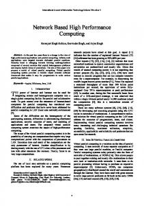
Hardware Assists for High Performance Computing Using a Mathematics of Arrays H. Pottinger, W. Eatherton, J. Kelly Department of Electrical Engineering L. R. Mullin, T. Schifelbein Department of Computer Science University of Missouri - Rolla Abstract -- Work in progress at the University of Missouri Rolla on hardware assists for high performance computing and communication is presented. This research consists of a field programmable gate array based rapid prototyping environment (Chameleon) being used to evaluate hardware architectures for speedup of array partitioning and routing algorithms. These algorithms have been developed using a Mathematics of Arrays (MOA) and are optimal in the sense that they reduce normal array indexing operations to a series of primitive additions based on array shape. The method is simple yet powerful, produces algorithms which are provably correct, and are independent of dimensionality. Software implementations have been used to provide speedups on the order of 100% to the solution of heat transfer equations on a uniprocessor. 1. Introduction All serious computer applications involve the communication of as well as computations on large data structures. So called lazy evaluation of expressions exploited in modern functional languages seek to minimize operations by simplifying expressions and performing evaluations only when values are needed. Unfortunately support for operations on large arrays is somewhat lacking. In order to produce efficient code one must avoid the repeated copying of large arrays which could otherwise simply be updated in place. Functional languages on the other hand require that operators create new result objects from input operands rather than update operands in place in order to keep operations free of side effects. The Psi Calculus is a new Mathematics of Arrays (MOA) which provides a formal way of describing data parallel computations with minimum I/O and computational complexity. It specifies array operations as manipulations of shapes in a dimension independent way, permits sequences of structuring operations to be condensed, avoids creating temporaries, and provides a scheme for statically partitioning array operations in a balanced form over arrays of processors. Through the use of the Ω operator it can be extended to become a full fledged functional calculus. The Psi Calculus is defined in [1] and is based on Abrams' work on the simplification of array expressions [2]. We review MOA operations and briefly show how they can be applied to the partitioning and routing of arrays on parallel computers. We then describe a basic hardware structure for speeding up MOA operations and show how a prototype is being constructed by using a combination of high level synthesis and field programmable logic. We conclude with some observations on the future of this work in high performance computing.
2. An Introduction to MOA This section presents a brief introduction to the main operators used in a Mathematics of Arrays. The complete reference for MOA can be found in [1]. The examples are not complete definitions and are intended mainly to help the reader understand the basic concepts involved. The two dimensional array L1
2 3O P 4 N 5 6Q
ξe 2 ≡ M
will be used as a running example throughout this section. Table I summarizes some of the basic operations. The notation is used to indicate a constant vector of two elements. Table I. Some MOA Operators Operator
δ ρ τ π
Function Number of dimensions Shape
∆
Number of elements Product of vector elements Take (subarray)
∇
Drop (subarray)
ι
Count (iota)
rav
Flatten an array
ψ
Index function
γ
Offset
Example
δξe = 2 ρξ e = 2 3 τξe = 6 πρξe = 6
1∆ξ e = 1 2 3 1∇ξ e = 4 5 6 ι4 = 0 1 2 3 ravξ e = 1 2 3 4 5 6 1 0 ψξ e = 4 γ( 1 0 ; 2 3 ) = 3
The γ operator forms a correspondence between ψ and rav defined as r
r
( ravA n )[ γ ( v ; ρA n )] = v ψA n r
where A n is an n dimension array, and v is a valid index vector. γ thus forms an index into the flattened array given a valid index vector and the shape of the array. Pointwise extensions to the familiar relational operations are defined. For example, the expression r
0 ≤ * i < * ρξ
is commonly used and is understood to mean that every element r of vector i is greater than or equal to 0 and less than the corresponding element of the shape of array ξ. Pointwise operations are also commonly used. For example A * B where ρA = ρB is defined as the scalar product of every element of A with every corresponding element of B and should not be confused with the familiar matrix multiplication. The Ω operator applies either a unary or binary operator to subarrays of one or two argument arrays. For example + red Ω ξ 2e partitions ξ into its two one dimensional row vectors and applies the sum reduction operator to produce 6 15 . The expression ξ e2 + Ω < 0 2>ξ e2 partitions the left array into its 6 scalar components and the right array into a single 2d copy of itself and then applies the + operator pointwise by adding each scalar to every component of the rightmost array. The formal definition of Ω is complex and can be found in [1]. As an example familiar matrix multiplication can be expressed in MOA notation as:
C = +red ( Ω ( Α[*Ω ]Ω Β) where ρA =< n p > , ρB =< p m > , and ρC =< n m > . The two rightmost omega operators multiply each of the p rows of B by the n*p components of A and the leftmost omega operator applies the sum reduction operator to each of the n*m 2d subarrays of the result to produce array C. Expressions such as this can be transformed using the theorems of the Psi Calculus to produce simpler expressions which are optimal in the sense of minimal I/O and computation requirements in a portable, scalable, architecture independent fashion. These transformations have been partially mechanized in the Psi Compiler [3]. 3. Psi Compiler The Psi Compiler is an ongoing project intended to mechanize the process of using the Psi Calculus to reduce array expressions so as to eliminate unnecessary computation and temporary storage. The Psi Compiler is independent of the source or destination language and versions exist for both C and High Performance Fortran (HPF). Preliminary versions are available via Mosaic at http://sunserver.cs.umr.edu/psi/psi.html. The compiler has been used to produce code which exhibits significant speedup on both uni and distributed processors compared to conventional coding techniques. 4. Hardware Acceleration Although the Psi Compiler has been used effectively to speedup conventional software computation on arrays it seems desirable to examine hardware solutions for achieving even higher performance. A reasonable approach appears to be a rapid prototyping environment in which various approaches can be tried. This is especially true since the compiler is still under development. Experience gained in previous projects with PC based multi-FPGA reconfigurable coprocessors led us to develop our own Sun workstation based coprocessor we call Chameleon. Chameleon consists of two large fast Xilinx field programmable
gate arrays (FPGA) for address computation, some onboard high speed static RAM (SRAM), and an Analog Devices ADSP-21020 Digital Signal Processor for high speed floating point calculations. The later was included in order to overcome the handicap of similar rapid prototyping systems which have no such floating point capability. Although the initial system is manually programmed our goal is to use the Psi Compiler to generate synthesizable VHDL code for high performance array address generation and microcode for floating point intensive computation by the DSP. The Chameleon Card is designed to follow the IEEE 14961993 SBUS specification. The card's interface to the SBUS is a Xilinx 4010 Field Programmable Gate Array with a "-5" speed grade rating. Due to the timing limitations of the grade of FPGA within the budget of this project, the maximum clock speed for the SBUS clock with this card is 20 Mhz. This limitation is in violation of the 1496-1993 specification but the test platform of this project (a SPARCstation- IPX) and most later models of SUN workstations operate the SBUS at 20 Mhz or less. FPGAs are currently available that could replace the "4010mq208-5" and meet all specifications including a maximum 25 Mhz clock. The width of the card for slave mode transfers is 8, 16, or 32 bits. In master mode the card currently uses 32 bit wide transfers with burst sizes of 1 ,2 , 4, 8, or 16 words. Direct virtual memory access (DVMA) is used for the transfers allowing the card to work independently of the Sun processor once configuration data is sent to the board. Fig. 1, shows a sample 2 word, 32 bit burst transfer. As can be seen the transfer begins with a bus request by the card, the cycle continues with the bus grant from the SBUS controller. The cycle after the bus grant, the master controller on the card puts the virtual address of the memory location being accessed along with the size of the transfer( 2, 4, 8, or 16 words), and uses the 'RD' line to indicate a read or write. On a write, the master card puts the first word being written onto the bus on the cycle following the placement of the virtual address. Then the master waits until the SUN memory signals a successful write with an appropriate response on the 'ACK[2:0]' bus. On a read, the master waits for the SUN memory to drive the SBUS with the appropriate data from the indicated read address. Then when the 'ACK[2:0] bus signals the data is ready, the master latches in the word. Fig. 1 shows a burst cycle that has two wait states inserted into the transfer of both words by the slave. Therefore it takes nine clock cycles to transfer two words or 8 bytes. Performance estimations can be made for the card's bandwidth using the SUN IPX as an example of a low end platform for Chameleon. Since the card is planned to be used for computations involving large arrays stored somewhat contiguously in memory, the card will be able to use the 16 word transfer mode. Assuming an immediate response to the bus request, it will take a total of 21 clock cycles to transfer 16 words of data. This is due to an added cycle for address translation and another added cycle for the transfer of the first word in the burst. Therefore, 64 bytes are transferred in 21 clock cycles. Using the IPX SBUS clock speed of 20 Mhz, this results in a 61 Mbyte/second transfer rate. While this is a relatively high bus transfer rate, Chameleon's DSP running at 100 MFLOPS could potentially tie up a bandwidth of 1.2 Gbytes/second with a stream of calculations consisting of 2 input variables and one output variable. Therefore, care was taken in the board's design to saturate the SBUS as much as possible.
Fig. 2 shows a block diagram of the Chameleon board with the main emphasis being on the data flow. The interface chip contains double buffer from and into the SBUS data bus. These double Buffers and are FPGA SRAMS constructed from the configurable logic blocks that normally create the look up tables for logic functions in the FPGA. The 4.5 ns internal access time of the SRAM is one of the many advantages to the FPGA implementation of the interface chip. Another advantage is the ease of synthesis from VHDL to a partitioned and routed chip. A process that takes hours not weeks like with conventional ASICS. Additionally in the debugging and application stage of the board use, changes to the interface chip can be taken from high level VHDL testing to actual implementation in a matter of hours. The Boot EPROM shown in Fig. 2 is for initial configuration of the FPGA on power up, and the ID EPROM shown is for the initial configuration of the SBUS on power up via a series of slave read from the board starting at address 0. In addition to the interface FPGA in Fig. 2, two peripheral FPGAs labeled X1, and X0 are shown along with the DSP chip. The two additional FPGAs are programmed through the SBUS and are used for the control of the DSP chip, and the manipulation of data between the SBUS, CMOS SRAMs, and the DSP chip. Using the flags, interrupts, and DSP polling techniques, the DSP chip can be used as a highly pipelined floating point coprocessor. Notice that following the counterclockwise data path movement, the data flows into the DSP from the Data Bus path and flows out of the DSP chip through the Program Bus path. This is possible without delays due to a internal program cache that stores any instructions that conflict with a data movement on the Program Bus. Since most common computations performed on matrices involve more input variables than output variables, placing the output data on the Program Bus was a logical choice. While placing all data movement on the Data Bus also avoids instruction conflicts, the data flow would no longer be circular through the board and it might not have been possible to achieve as much parallelism in the interface chip design. Currently up to three data movement processes can be concurrently running. For instance, in the same clock cycle the X1 FPGA could be loading to one of the 16x32 buffers while the other buffer is doing a burst transfer on the SBUS. Concurrently one of the input buffers could be unloading to the X0 FPGA. In addition to the above mentioned functions, the interface chip also traps and reports a wide of variety of errors from master errors, slave errors, to errors while programming the two peripheral FPGAs. 5. An Example: Array Convolution Array convolution is useful for many applications involving finite difference methods on array data sets. Such applications include heat transfer, and field analysis, as well as audio and video signal processing. The implementation of a fast array convolution coprocessor involves several concepts from a Mathematics of Arrays. The design will use MOA to derive a hardware algorithm for optimal memory address generation. Use of this algorithm will insure that the array convolution computation in hardware will be optimal for all the resources involved (bus bandwidth, DSP speed, supporting architecture, data shapes, etc.). To perform an array convolution, an initial data array must be defined as well as a multiplier mask. This mask will be
applied to all sets of points in the data array to compute the resultant data array with boundary conditions held constant. This process can be iterated until the difference between iterations for all points is less than some predefined epsilon or until a predetermined iteration count is reached. Heat transfer or field analysis applications normally use the method of finite difference. Alternately a single iteration may be performed on an image to achieve a desired effect like smoothing or edge detection via filtering. With these applications in mind, only 1, 2 and 3 dimensional data arrays will be supported. With a given mask, any conceivable convolution can be performed. The mechanics of the array convolution are simple. An example will be given with a 3x3 multiplier mask on a 2 dimensional data array. A single resultant point in the resultant data array is computed by taking each element of the mask and multiplying with each element of a corresponding region in the data array centered about the point of interest and summing the results to compute the resultant point. This is repeated for all points in the initial data array until all the points in the resultant data array are found. For example, a mask M with shape defined as:
ravM = m0 m1 m2 m3 ... m8 2
and a data array D with a shape of defined as:
ravD =< d 0 d1d 2 ... d τD −1 > 2 and a 2 dimensional resultant data array R with a shape of defined as:
ravR =< r0 r1r2 ... rτR −1 > will require a computation of
R = +redTi2 where r
r r
Ti2 = i ψΜ *(b ∆i ∇D ) r
r
∀ 0 ≤ * i < * ρM
and b =< 98 98 > . This concisely expresses array convolutions in a manner suitable for computation on either a uniprocessor or parallel processor. This process can be expanded to even more dimensions, for example, a 3 dimensional heat flow simulation over time. Chameleon's FPGAs will be used to implement the address generation algorithm. The design will be created with VHDL and synthesized using Mentor Graphics Autologic. MOA will be used to create an address generation algorithm that optimally uses the S-Bus for DVMA transfers of the initial and resultant data arrays. With optimal use of the S-Bus bandwidth, a fast array convolution hardware coprocessor can be realized. Verification of the system's efficiency can be found by examining S-Bus saturation and if the initial and resultant data arrays are accessed with minimum reads and writes. Several factors can be examined in the course of creating an optimal array access algorithm. First, array access must be at
a minimum. The best case is when each data element in the initial and final data arrays is accessed only once and the S-Bus is saturated by the coprocessor system. With an average bus transfer rate of 60 MB/s, a convolution of a 50x50x50 array (125,000 elements) of 32 bit floating point numbers will take only 16.7 ms to complete one iteration and 8.33 s to complete 500 iterations. This compares to a classical software approach that took a little over 1417 s to complete 500 iterations and an MOA optimized software algorithm that took over 474 s to complete 500 iterations. As a designer for a coprocessor system like this, the only part that can be controlled is the order in which the elements in the data arrays are accessed. Using MOA, this order can be optimized to minimize data access. It is unlikely that the arrays can be accessed such that each element is accessed only once. This may be the case for writing the resultant array, so the problem really lies in reading the initial data array. Using MOA, an optimal memory access pattern can be generated for this purpose. Factors influencing this derivation include burst transfer sizes, local memory sizes, data array shapes, and mask shapes so cost functions must be developed to model the system's behavior. Weighing all these factors together will aid in creating an address generation algorithm that optimally accesses the data arrays and provides for a system realization that performs a provably correct fast array convolution.
Fig. 1 SBUS Timing Diagram
6. Conclusion A Mathematics of Arrays is an excellent tool for visualizing and expressing operations on arrays. Reductions on the resulting algorithms can be performed mechanically to reduce the amount of address calculation and temporary storage requirements. The resulting simplified address generation computation is suitable for realization in hardware for driving a fast floating point coprocessor. A hardware accelerator for a Sun IPX workstation consisting of a pair of reconfigurable FPGA's and a high speed DSP is being constructed to support this effort. A compiler for mechanizing Psi Calculus reductions has been developed with good initial results and is being extended to support the hardware accelerator. Acknowledgments The authors would like to acknowledge the generous support of Xilinx and Analog Devices. We are also grateful for the funding provided by the UM-Rolla's OURE program.
References [1] Mullin, Lenore, "A Mathematics of Arrays", Ph. D. dissertation, Syracuse University, December 1988. [2] Abrams, P.S. "What's wrong with APL", in APL 75, ACM, June, 1975. [3] Mullin, L., Thibault, S., "A Reduction semantics for array expressions: the PSI compiler", TR CSC-94-05, March 9, 1994, Department of Computer Science, University of Missouri - Rolla.
Fig. 2 Chameleon Board Block Diagram