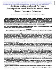
First International Engineering Conference (IEC2014)
Hardware Implementation of a Two-way Superscalar RISC Processor using FPGA Safaa S. Omran 1, Ali J. Ibada 2 College of Electrical and Electronic Techniques, Baghdad, Iraq 1
[email protected] ,2
[email protected]
ABSTRACT Previous researches were focused on designing single cycle processors or pipeline processors by FPGA (Field Programmable Gate Array). This research is a new trend in this field. Superscalar processor can execute various parallel instructions per cycle. This microarchitecture exploits Instruction Level Parallelism (ILP) available in a program. In this paper a two-way Superscalar processor is designed. First a Single cycle 32-bit MIPS (Microprocessor without Interlocked Pipeline Stages) RISC (Reduced Instruction Set Computer) processor designed by defining MIPS ISA (Instruction Set Architecture), and dividing the Processor into two parts: the datapath unit, and the control unit. Then two-way Superscalar Processor is designed, it consists of two Single cycle Processors shared Registers and Hazard unit. Next, a top level is implemented by connecting data and instruction memories to the processor. The VHDL (Very high speed integrated circuit Hardware Description Language) hardware modeling is used. The Superscalar and top level is designed using (Xilinx ISE Design Suite 13.4) Software. This modeling is configured on FPGA Spartan-3AN starter kit and results from the kit were obtained. Keywords: Superscalar, MIPS, ISA, RISC, VHDL, FPGA. 1. INTRODUCTION Superscalar is a processor architecture contains multiple copies of the datapath hardware to execute multiple instructions simultaneously. Recall that parallelism comes in temporal and spatial forms. Multiple execution units are a case of spatial parallelism [1]. The RISC processor had fixed-length instructions based on three different formats (R-type, I-type and J-type). It is designed to perform a smaller number of types of computer instructions so that it can operate at a higher speed. The only operations that affect memory are load and store operations that move data from memory to a register or from a register to memory, respectively, so that it is called load-store architecture [2]. Single cycle MIPS is a RISC processor that can execute an entire instruction in one cycle. The cycle time is limited by the slowest instruction. Many previous researches have implemented the simple design of a single cycle RISC processor in FPGA. Reaz, Jalil, and Rahman [3], Anjana and Krunal [4] performed the simple design of MIPS processor which can execute basic instructions (less than 12 instructions). Rubio [5] implemented a Single cycle and pipeline MIPS processor which can execute 15 instructions. Safaa S. Omran and Hadeel S. Mahmood [6] designed a single cycle RISC processor that can execute almost all instruction of MIPS processor. Kumar and Begum [7] designed the 5-stage pipeline architecture of the 32-bit MIPS processor. While Anthony [8] made a VHDL model of Pipelined DLX processor. In this research Superscalar processor is designed and implemented for whole MIPS instructions (49 instructions), also hlt instruction was added to stop program execution. 145
First International Engineering Conference (IEC2014)
As clarified references that were read in this specialization, this work is the first design that had design and implementation a Superscalar processor in FPGA. VHDL describes the behavior of an electronic circuit or system, such as ASICs (Application Specific Integrated Circuit) and FPGAs as well as conventional digital circuits. A fundamental motivation to use VHDL is that VHDL is a standard, technology/vendor independent language, and is therefore portable and reusable [9].VHDL has Feature to allow the synthesis of a circuit or system in a programmable device. This paper studies the designing and prototyping of a complete Superscalar MIPS RISC processor in VHDL. FPGAs are digital integrated circuits (ICs) that contain configurable (programmable) blocks of logic along with configurable interconnects between these blocks. Design engineers can configure (program) such devices to perform a tremendous variety of tasks [10]. 2. INSTRUCTIONS SET ARCHITECTURE The first step in understanding any computer architecture is to learn its language. The words in a computer’s language are called instructions. The computer’s vocabulary is called the instruction set. All programs running on a computer use the same instruction set. All instructions in RISC processor have the same length and have a single instruction format. MIPS processor uses 32-bit instructions and defines three instruction formats as shown in Table 1: TABLE 1. Formats of MIPS instructions Field size R-Type I-Type J-Type
6-Bit op op op
5-Bit rs rs
5-Bit rt rt
5-Bit rd
5-Bit shamt imm
6-Bit funct
addr
Where: op: basic operation of the instruction, traditionally called the opcode. rs: the first register source operand. rt: the second register source operand. rd: the register destination operand, it gets the result of the operation. shamt: shift amount, it is used in shift instruction to hold shift amount. funct: function, it selects the specific variant of the operation in the op field. imm: the 16-bit address which is used in data transfer instructions. addr: the 26-bit address which is used in jump instructions. 3. PROCESSOR DESIGN The complete design of a 32-bit, Two-way Superscalar MIPS processor consists of six interacting parts: 1. Two 32-bit datapaths. 2. Two control units. 3. Register file. 4. Hazard unit. This design can perform all operation that Single cycle MIPS processor can do (50 instructions). 146
First International Engineering Conference (IEC2014)
3.1 32-BIT DATAPATH Two-way Superscalar contains two copies of hardware to execute two instructions simultaneously. Figure 1 shows a block diagram of datapaths of twoway superscalar processor that fetches and executes two instructions per cycle. The datapaths fetches two instructions at a time from instruction memory.
FIGURE 1. Superscalar datapaths
Each datapath contains elements such as memories, multiplexers, sign and zero extenders. A description of each datapath element is given below: 1. Program counter (PC): is 32-bit register. Its output (PC) represents the address of the current instruction (instr) to be executed. 2. Instruction memory takes a 32-bit address from PC register and read a 32-bit data. 3. Data memory has one output read port (RD) and one input write port (WR). 32-bit data at input (WR) port is written to memory location specified by the address (A). 4. Multiplexers are used to select one output from several inputs. 5. Sign extender simply copies the sign bit to all of the upper word output. 6. Zero extender takes a half word or byte and simply puts zeros in all of the upper word output. 7. ALU (arithmetic logic unit) has been designed in order to execute all the arithmetic-logical instructions. Figure 2 shows ALU. Table 2 illustrates functions that can be executed by the ALU.
FIGURE 2. The Extended ALU
147
First International Engineering Conference (IEC2014)
TABLE 2. Functions of ALU Alucontrol (5:0)
function
000000 000001 000010 000011 000100 000101 000110 000111 001000 010000 010001 010010 010011 010100 010101 010110 100100 100111 101000
A and B A or B A+B Not used Sll A xor B A nor B Srl Sra A & B’ A or B’ A–B Slt Not used A xor B’ A nor B’ Sllv Srlv Srav
9. Mul/div unit performs signed/unsigned multiplication and division. It takes two inputs of 32 bits (A and B) and produce (y) output of 64 bits, if sign is 1 then signed operation will be performed, otherwise it will perform unsigned operation. When mult input is 1 and div is 0, Y(63:0)=A*B and when mult is 0 and div is 1, Y(31:0)=a/b and Y(63:32)= remainder. Then Y(63:32) is stored at hi register while Y (31:0) is stored at lo register. 3.2 CONTROL UNIT The Control unit receives opcode (instr 31:26) and funct (instr5:0) fields of the current instruction from the datapath to provide multiplexers select control signals, memory write signal, register write signal and control signals of ALU and mul/div unit. It consists of two parts: main control and R-type control. The meanings of ALUop signals are giving in Table 3. Main control uses opcode (instr 31:26) field as inputs and produce multiplexers select control signal, memory write, register write and 3-bit ALUop signals as shown in Table 4. TABLE 3. ALUop meaning Aluop 000 001 010 011 100 101 110 111
Meaning Add Sub And Or Xor Slt Look at funct field N/a
148
First International Engineering Conference (IEC2014)
R-type control used ALUop signals with funct (instr 5:0) field of instruction to produce ALUcontrol (5:0) signals and several signals used in the execution of Rtype instructions.
TABLE 4. Main control truth table Regdst
Alusrc
Branch
Brchne
Blez
Bltz
Bgtz
01 00 xx xx xx xx xx xx 00 00 xx 10 00 00 00 00 00 00 00 00 00 00 xx xx xx
00 01 01 00 00 00 00 00 01 01 xx xx 10 10 10 01 01 11 01 01 01 01 01 01 xx
0 0 0 1 0 0 0 0 0 0 x x 0 0 0 0 0 0 0 0 0 0 0 0 x
0 0 0 0 1 0 0 0 0 0 x x 0 0 0 0 0 0 0 0 0 0 0 0 x
0 0 0 0 0 1 0 0 0 0 x x 0 0 0 0 0 0 0 0 0 0 0 0 x
0 0 0 0 0 0 1 0 0 0 x x 0 0 0 0 0 0 0 0 0 0 0 0 x
0 0 0 0 0 0 0 1 0 0 x x 0 0 0 0 0 0 0 0 0 0 0 0 x
0 0 1 0 0 0 0 0 0 0 0 0 0 0 0 0 0 0 0 0 0 0 1 1 0
00 01 xx xx xx xx xx xx 00 00 xx xx 00 00 00 00 00 00 11 11 10 10 xx xx xx
hlt
Regwrit e 1 1 0 0 0 0 0 0 1 1 0 1 1 1 1 1 1 1 1 1 1 1 0 0 0
ALUop
S_zext x x x x x x x x x x x x x x x x x x 0 1 0 1 x x x
Jal
Sh_B xx xx 11 xx xx xx xx xx xx xx xx xx xx xx xx xx xx xx xx xx xx xx 00 01 xx
Jump
Opcode 000000 100011 101011 000100 000101 000111 000001 000110 001000 001001 000010 000011 001100 001101 001110 001010 001011 001111 100000 100100 100001 100101 101000 101001 111100
Memtor eg Memwr ite
Instruct ion R_type lw sw beq bne blez bltz bgtz addi addiu j jal andi ori xori slti sltiu lui lb lbu lh lhu sb sh hlt
0 0 0 0 0 0 0 0 0 0 1 1 0 0 0 0 0 0 0 0 0 0 0 0 x
0 0 0 0 0 0 0 0 0 0 0 1 0 0 0 0 0 0 0 0 0 0 0 0 x
110 000 000 001 001 001 001 001 000 000 xxx xxx 010 011 100 101 101 000 000 000 000 000 000 000 xxx
0 0 0 0 0 0 0 0 0 0 0 0 0 0 0 0 0 0 0 0 0 0 0 0 1
3.3 REGISTER FILE It consists of 32 registers each of 32-bit in size. The register file's ports were duplicated. It has four read ports (RD1, RD2, RD3, and RD4) and two write port (WD3, WD6). Register file used ports (RD1, RD2, WD3, A1, A2, and A3) to communicate with 32-bit datapath 1, and signal WE1 is provide from control unit 1 to Register file, this consider entire processor 1. Also it is used ports (RD3, RD4, WD6, A4, A5, and A6) to communicate with 32-bit datapath 2, and signal WE2 is provide from control unit 2 to Register file, this consider entire processor 2. Figure 3 shows the complete design of a single datapath and the control unit connected to register file and memories.
149
First International Engineering Conference (IEC2014)
FIGURE 3. complete design of a single datapath and the control unit
3.4 HAZARD UNIT Hazard unit is needed to control flow program correctly. It manages data dependency between MIPS processor 1 and MIPS processor 2. If hazard unit detects dependency it sends stall signal to MIPS processor 2 to keep it in stall state. Stall signal manage regwrite and memwrite signals in MIPS processor 2. If stall signal is 0 then regwrite and memwrite signals take its values from control unit in MIPS processor 2, if stall signal is 1 then these two signals (regwrite and memwrite) become zero. When regwrite and memwrite equal zero, any operation in MIPS processor 2 will not save the result. This keeps MIPS processor 2 in stall state. Table 5 shows when stall occurred. TABLE 5. Stall in superscalar processor Instruction 1 jump, jal, jr, jalr beq, bne, blez, bltz, bgtz
Instruction 2
Condition
don’t care
no condition
lw, lh, lhu, lb, lbu
sw, sh, sb
sw, sh, sb
lw, lh, lhu, lb, lbu
any instruction
any instruction
when Both instructions accessing to the same address in data memory when Both instructions accessing to the same address in data memory If register destination [rd]in instruction 1 used as source in instruction 2, or if register destination [rd] in instruction 2 used as source in instruction 1.
3.5 VHDL TOP-LEVEL IMPLEMENTATION Top level of two-way Superscalar design connects all components of Superscalar (32-bit datapaths, Control units, Register file, and Hazard unit) to external separate instruction and data memories through the data and address busses. Figure 4 demonstrates Superscalar MIPS processor interfacing with data and instruction memories. Data and instruction memories size is 256 byte hold 64 words of 32-bit. Test bench is written to test the Superscalar MIPS processor and show simulation of program’s execution before configuring FPGA.
150
First International Engineering Conference (IEC2014)
FIGURE 4. Superscalar processor connected to external memories
4. RESULTS Program in Figure 5 used to calculate Fibonacci sequence {1, 1, 2, 3, 5, 8, 13, etc.} for first 40 number and save resulting sequence in data memory at address [0: 39]. It is stored in instruction memory.
loop:
Assembly addi $t6, $zero, 1 addi $t7, $zero, 4 sw $t6, 0($zero) sw $t6, 0($t7) addi $t9, $zero, 9C addi $t0, $zero, 8 addi $t3, $t0, -8 addi $t4, $t0, -4 lw $t1, 0($t3) lw $t2, 0($t4) add $t5, $t1, $t2 addi $t0, $t0, 4 sw $t5, -4($t0) slt $t8, $t9, $t0 beq $zero, $t8, loop hlt
Address Description $t6 = 1 0 $t7 = 4 4 mem[$zero + 0] = $t6 8 mem[$t7 + 0] = $t6 c $t9 = 9C 10 $t0 = 8 14 $t3 = $t0 + -8 18 $t4 = $t0 + -4 1c $t1 = mem[$t3 + 0] 20 $t2 = mem[$t4 + 0] 24 $t5 = $t1 + $t2 28 $t0 = $t0 + 4 2c mem[$t0 + -4] = $t5 30 if ($t9 < $t0) $t8 = 1 else $t8 = 0 34 if $zero = t8 then go to -9 38 stop program 3c FIGURE 5. Fibonacci sequence test program
Machine 200E0001 200F0004 AC0E0000 ADEE0000 2019009C 20080008 210BFFF8 210CFFFC 8D690000 8D8A0000 012A6820 21080004 AD0DFFFC 0328C02A 1018FFF7 F0000000
By using testbench, this program was executed and the results are shown in Figure 6. As long as memwrite signal is 1, the results are stored at data memory. For first 40 number of Fibonacci sequence the last value is "06197ecb"h stored at address (9c)h in data memory.
151
First International Engineering Conference (IEC2014)
FIGURE 6. Superscalar MIPS simulation waveform of Fibonacci sequence program
This design is configured on Xilinx Spartan-3AN starter kit FPGA. PC screen is interfaced with FPGA to show all results. Figure 7 shows results of Fibonacci sequence test program on PC screen.
FIGURE 7. Results of Fibonacci sequence program on PC screen
CONCLUSION VHDL design of MIPS RISC processor for Superscalar processors had been implemented for whole instructions which consist of 49 instruction. Also hlt instruction was added to processors to stop program execution. After design was completed, various programs are simulated by using (Xilinx ISE Design Suite 13.4) and results from the kit were obtained. It is meaning that design work properly. Superscalar processor used extra hardware to build it, this extra hardware charge extra cost at manufacturing, but these extra cost result superscalar processor with better performance.
152
First International Engineering Conference (IEC2014)
REFERENCES [1] [2] [3]
[4]
[5]
[6]
[7]
[8] [9]
Harris D., Harris S., "Digital Design and Computer Architecture", Morgan Kaufmann, San Francisco, USA, 2007. Hennessy J., Patterson D., “Computer Architecture: A Quantitative Approach”, Morgan Kaufmann, San Francisco, USA, 2007. Reaz M. B. I., Jalil J., Rahman L. F., “Single Core Hardware Modeling of 32Bit MIPS RISC Processor With A Single Clock “, Research Journal of Applied Sciences, Engineering and Technology, Vol.4, No.7 , pp.825-832, 2012. Anjana R., Krunal G., “ VHDL Implementation of a MIPS RISC Processor”, International Journal of Advanced Research in Computer Science and Software Engineering, Vol. 2, No.8, pp.83-88, 2012. Robio V., “A FPGA Implementation of A MIPS RISC Processor for Computer Architecture Education”, MSc. Thesis, New Mexico State University, Las Cruses, New Mexico, America, 2004. Safaa S. Omran, Hadeel S. Mahmood, "Hardware modelling of a 32-bit, single cycle RISC processor using VHDL", ICIT 2013 The 6th International Conference on Information Technology, May 8, 2013. Kumar M. K., Begum MD. S., "FPGA based implementation of 32 bit RISC processor", International Journal of Engineering Research and Applications, Vol. 1, NO 3, pp.1148-1151. Anthony I., “VHDL Implementation of Pipelined DLX Microprocessor”, MSc. Thesis, University Technology Malaysia (UTM), Malaysia, 2008. Pedroni V., “Circuit design with VHDL”, MIT Press, London, England, 2004.
[10] Maxfeild C., "The Design Warrior's Guide to FPGAs: Devices Tools and Flows", Elsevier, USA, 2004.
153