tical clock signal pulses, the timing jitter of the retimed data optical data .... edged for the financial support I received for my external research stay at. UCSB. ...... Furthermore, if we assume that the noise drive terms dnj are independent.
High-Speed Clock Recovery and Demodulation using Short Pulse Sources and Phase-Locked Loop Techniques
Darko Zibar
May 2007
COM•DTU Department of Communications, Optics & Materials Technical University of Denmark Building 345V 2800 Kgs. Lyngby DENMARK
2
Abstract We present a modelling technique and noise analysis of a clock recovery scheme based on an optoelectronic phase-locked loop. We treat the problem using techniques from stochastic processes and stochastic differential equations. A set of stochastic differential (Langevin) equations describing the optoelectronic phase-locked loop are derived. By using small-signal analysis, the Langevin equations are linearized and the associated system of stochastic differential equations is solved using Fourier techniques. Numerical simulations are then used to investigate the performance of the optoelectronic phase-locked loop with noise at a bit-rate of 160 Gb/s. It has been shown that it is important to reduce the time delay in the loop since it results in the increased timing jitter of the recovered clock signal. We also investigate the requirement for the free-running timing jitter of the local electrical and optical oscillator. We show that it is possible to obtain recovered clock signal with less timing jitter then the input data signal as long as the jitter of the free-running electrical oscillator is less than the input data signal timing jitter. Using the guidelines form the numerical simulations, optoelectronic phase-locked loop based clock recovery operating at 320 Gb/s is demonstrated. Optical regenerator with clock recovery, based on an optoelectronic phaselocked loop, is also described using techniques from stochastic calculus. An analytical expression for the power spectral density of the retimed data signal is derived. We use numerical simulation to investigate the performance of the optical regenerator operating at 40 Gb/s and 160 Gb/s. We have shown that for flat-top input data signal pulses and sufficiently narrow optical clock signal pulses, the timing jitter of the retimed data optical data signal can be significantly reduced compared to the jitter of the degraded input data signal. The optical clock signal pulse width needs to be relatively short compared to the optical data signal pulse width in order for the retimed data signal timing jitter to coincide with the recovered clock 3
timing jitter, i.e. 3.5 ps at 40 Gb/s and 0.5 ps at 160 Gb/s. In the last part of the thesis, a novel phase-locked coherent optical phase demodulator with feedback and sampling, to be used in phase-modulated radio-over-fibre optical links, is also presented, theoretically investigated and experimentally demonstrated. It is experimentally shown that the proposed approach results in 18 dB of spur-free-dynamic-range improvement compared to a traditional demodulator without feedback. A new time-domain, large signal, numerical model of the phase-locked coherent demodulator is developed and shown to be in excellent agreement with experimental results. Numerical simulations are used to investigate how loop gain, LO phase-modulator non-linearities, amplitude modulation, amplitude and timing jitter influence the dynamical behavior of the demodulator in terms of the signal-to-intermodulation ratio and signal-to-noise ratio of the demodulated signal. Furthermore, in order to alleviate non-linearities associated with the LO phase-modulator, we report on a novel technique for cancelation of the 3rd order intermodulation product of the demodulated signal. The proposed cancelation technique does not depend on input RF signal power and frequency.
4
Resum´ e (in Danish) Denne afhandling drejer sig om modelleringsteknik og støjanalyse i forbindelse med klokgendannelsessystemer, som er baseret p˚ a en optoelektronisk fasel˚ ast sløjfe. Der er brugt teknikker fra stokastiske processer og stokastiske differentialligninger til at løse problemet. Stokastiske differentialligninger, der beskriver en optoelektronisk fasel˚ ast sløjfe, bliver udledt. Der er anvendt smøsignalanalyse til at linearisere ligningssystemet, og det fremkomne ligningssystem bliver løst ved hjælp af Fourier transformationsteknikker. Endvidere er der udført numeriske simuleringer for at undersøge virkem˚ aden af en optoelektronisk fasel˚ ast sløjfe ved 160 Gb/s. Det vises, at det er vigtigt at reducere tidsforsinkelsen inde i sløjfen, da der ellers vil opst˚ a forøget støj p˚ a det gendannede kloksignal. Endvidere undersøges kravene til de lokaloscillatorer, der indg˚ a i sløjfen. Det vises, at hvis den elektriske oscillator i sløjfen har mindre støj end det indkommende datasignal, s˚ a kan man stadigvæk opn˚ a støjreduktion, selv om den optiske lokaloscillator har mere støj end det indkommende datasignal. Ved at følge retningslinier fra teorien demonstreres klokgendannelse fra et 320 Gb/s datasignal. Optisk regenerering med klokgendannelse beskrives ogs˚ a. Dette gøres ved hjælp af teknikker fra stokastisk teori, og endelig bliver udledt et analytisk udtryk for frekvensspektret af det regenererede datasignal. Dernæst udføres numeriske simuleringer for at undersøge en optisk regenerator, der arbejder ved enten 40 Gb/s eller 160 Gb/s. Det vises, at det indkommende datasignal skal have firkantede pulser for at en væsentlig støjreduktion kan opn˚ as. Klokpulserne skal have en bredde i tid p˚ a 3.5 ps og 0.5 ps for systemer, der arbejder ved henholdsvis 40 Gb/s og 160 Gb/s for at støjen p˚ a det regenererede datasignal er lige s˚ a lille som støjen fra kloksignalet. I sidste del af afhandlingen bliver en ny fasel˚ ast, kohærent og optisk fasedemodulator med tilbagekobling samt sampling og beregnet til fasemodulerede optiske forbindelser præsenteret, teoretisk undersøgt og eksperimentelt demonstreret. Det vises eksperimentelt, hvordan den nye fasel˚ aste demodulai
tor giver en forbedring p˚ a 18 dB i dynamisk omr˚ ade sammenlignet med en traditionel fasedemodulator uden tilbagekobling. Endvidere er en ny tidsdomæne numerisk model blevet udviklet, og den vises at give resultater, som er i god overensstemmelse med eksperimentelle data. Numeriske simuleringer bruges til at undersøge, hvordan sløjfeforstærkning, ikke-linearitet i fasemodulatoren, amplitudemodulation, amplitude- og tidsjitter indvirker p˚ a signal-intermodulationsforholdet og signal-støj forholdet. Endelig præsenteres en ny lineariseringsteknik, som er uafhængig af RF signaleffekt og frekvens, og som derved kan overvinde fasemodulatorens ikke-linearitet.
ii
Acknowledgments It is a great pleasure and honor for me to thank my supervisors Prof. Palle Jeppesen, Prof. Jesper Mørk, Assistant Prof. Anders T. Clausen and Associate Prof. Leif K. Oxenløwe for their guidance and support throughout the project. They have all been a great inspiration and have contributed with invaluable help throughout the whole project. Their friendliness and kindness have made this whole period more pleasant and fun. Especially, I would like to thank Leif K. Oxenløwe for teaching me to do experimental work and for invaluable help not only with the experimental work but also with other technical issues. The experimental work presented in thesis could not have been completed without his help. Jesper Mørk is deeply acknowledged for invaluable help and discussions on mathematical issues. His constructive suggestions and contributions have had a positive reflection on the whole thesis. Bjarne Tromborg is also greatly acknowledged, his suggestions and help were crucial for some of the modelling work. I also enjoyed various technical discussions I had with Christophe Peucheret and Idelfonso Tafur Monroy. I would also like to thank Prof. John E. Bowers for accepting me as a Visiting Researcher at his Optoelectronics Research Group at the University of California, Santa Barbara (UCSB) and for introducing me to the field of microwave photonics. His guidance, support and enthusiasm are deeply reflected on the work I performed at UCSB. Collaborating with Leif Johansson, Hsu-Feng Chou and Anand Ramaswamy has also been a great pleasure. Leif’s creative approach to problem solving and willingness to help was greatly appreciated. Hsu-Feng Chou played a crucial role in bringing the theory and experiments together. I would also like to thank Prof. Roy Smith, Prof. Mark Rodwell, Prof. Larry Coldren, Larry Lembo and Matt Sysak for a number of stimulating and constructive discussions. I also thank Henrik N. Poulsen for great help with technical and non-technical issues while I was at UCSB. The seven months I spent in California will iii
remain an unforgettable experience that will influence me for the rest of my life. I would also like to thank the Danish Research Council for supporting this Ph.D. project. Danmark-America Foundation, FLSchmidt Koncern, Valdemar Selmer Trane and Elisa Trane foundation are all deeply acknowledged for the financial support I received for my external research stay at UCSB. Moreover, DARPA PHOR-FRONT program is acknowledged for travel support to the Coherent Optical Technologies (COTA) and the Microwave Photonics (MWP) conferences in 2006. I would also like to thank my present and former colleagues at COM for creating an excellent research environment: Emir Karamehmedovi´c, Michael Galili, Hans Christian Mulvad, Pablo H. Nielsen, Jesper B. Jensen, Yan Geng, Rasmus Kjær, Torger Tokle, Beata Zsigri, Brian Sørensen, Kresten Yvind, and Jeorge Seone. I also thank Majken Looms and my parents for great support and help during my whole Ph.D. period.
iv
Ph.D. publications Peer-reviewed journal papers: (6) [J1]
Darko Zibar, Jesper Mørk, Leif K. Oxenløwe and Anders T. Clausen, ”Phase noise analysis of clock recovery based on an optoelectronic phase-locked loop,” Journal of Lightwave Technology, vol. 25, no. 3, pp. 901–914, March 2007
[J2]
Darko Zibar, Leif A. Johansson, Hsu-Feng Chou, Anand Ramaswamy, Mark Rodwell and John E. Bowers, ”Dynamic range enhancement of a novel phase-locked coherent optical phase demodulator,” Optics Express, vol. 15, no. 1, pp. 33–44, January 2007
[J3]
Darko Zibar, Leif A. Johansson, Hsu-Feng Chou, Anand Ramaswamy, Mark Rodwell and John E. Bowers, ”Novel optical phase demodulator based on a sampling phase-locked loop,” Photonics Technology Letters, vol. 19, no. 9, pp. 686–688, May 2007
[J4]
Darko Zibar, Leif K. Oxenløwe, Hans Christian H. Mulvad, Jesper Mørk, Michael Galili, Anders T. Clausen, Palle Jeppesen, ”The effect of timing jitter on a 160 Gb/s demultiplexer,” Photonics Technology Letters, vol. 19, no. 13, pp. 957–959, July 2007
[J5]
Darko Zibar, Leif A. Johansson, Hsu-Feng Chou, Anand Ramaswamy, Mark Rodwell and John E. Bowers, ”Phase-Locked Coherent Demodulator with Feedback and Sampling for Optically Phase Modulated Microwave Links,” accepted for publication in Journal of Lightwave Technology, special issue on Microwave Photonics, 2008
[J6]
Hsu-Feng Chou, Anand Ramaswamy, Darko Zibar, Leif A. Johansson, Mark Rodwell, John E. Bowers and Larry Coldren,”Highlylinear coherent receiver with feedback,” Photonics Technology Letters, vol. 19, no. 12, pp. 940–942, June 2007 v
Peer-reviewed conference papers: (18) [C1]
Francesca Parmigani, Leif K. Oxenløwe, Michael Galili, Morten Ibsen, Darko Zibar, Perikles Petropoulus, David Richardson, Anders T. Clausen and Palle Jeppesen, ”All-optical 160 Gb/s RZ data retiming system incorporating a pulse shaping fibre Bragg grating,” in Proceedings of European Conference on Optical Communication 2007, Berlin, Germany, paper 5.3.1, 2007
[C2]
Leif Oxenløwe, Francesca Parmigani, Michael Galili, Darko Zibar, Anders T. Clausen, David Richardson, Morten Ibsen, Perikles Petropoulus and Palle Jeppesen, ”160 Gb/s retiming using rectangular pulses generated using a superstructured fibre Bragg grating,” in Proceedings of OptoElectronics and Communications Conference 2007, Yokohama, Japan, Paper 13B3-4, 2007
[C3]
Leif A. Johansson, Darko Zibar, Anand Ramaswamy, Larry Coldren, Mark Rodwell and John E. Bowers, ”Analysis of sampled optical phase-lock loops,” in Proceedings of International Topical Meeting on Microwave Photonics (MWP) 2007, Victoria Canada, paper Th4-32, 2007
[C4]
Darko Zibar, Leif K. Oxenløwe, Jesper Mørk, Anders T. Clausen and Palle Jeppesen, ”Analysis of the effects of pulse shape and width on the retiming properties of a 3R regenerator,” in Proceedings of European Conference on Laser and Electro-Optics (CLEO/Europe) 2007, Munich, Germany, paper CI2, 2007
[C5]
Darko Zibar, Leif A. Johansson, Hsu-Feng Chou, Anand Ramaswamy, Mark Rodwell and John E. Bowers, ”Investigation of a novel optical phase demodulator based on sampling phase-locked loop,” in Proceedings of International Topical Meeting on Microwave Photonics (MWP) 2006, Grenoble France, paper P1, 2006 (Best student paper award)
[C6]
Darko Zibar, Leif A. Johansson, Hsu-Feng Chou, Anand Ramaswamy and John E. Bowers, ”Time-domain analysis of a novel phaselocked coherent optical demodulator,” in Proceeding of Conference on Coherent Optical Technologies and Applications (COTA) 2006, Whistler, Canada, paper JWB1, 2006
[C7]
Darko Zibar, Jesper Mørk, Leif K. Oxenløwe, Anders T. Clausen and Palle Jeppesen, ”Reduction of timing jitter by clock recovery based on an optical phase-locked loop,” in Proceeding of Conference vi
on Laser Electro Optics (CLEO) 2006, Long Beach California, USA, paper CMJ4, 2006 [C8]
Darko Zibar, Leif K. Oxenløwe, Hans Christian H. Mulvad, Jesper Mørk, Michael Galili, Anders T. Clausen, Palle Jeppesen, ”The impact of gating timing jitter on a 160 Gb/s demultiplexer,” in Proceeding of Optical Fiber Communication Conference (OFC) 2006, Anaheim California, USA, paper OTuB2, 2006
[C9]
(invited paper) Leif K. Oxenløwe, Michael Galili, Hans Christian H. Mulvad, Anders Clausen, Darko Zibar and Palle Jeppesen, ”Solutions for ultra high-speed optical wavelength conversion and clock recovery,” in Proceedings of International Conference on Transparent Optical Networks (ICTON), Nottingham, United Kingdom, paper Tu.D2.3, 2006
[C10] Hsu-Feng Chou, Anand Ramaswamy, Darko Zibar, Leif A. Johansson, John E. Bowers, Mark Rodwell and Larry Coldren, ”SFDR improvement of a coherent receiver using feedback,” in Proceeding of Conference on Coherent Optical Technologies and Applications (COTA) 2006, Whistler, Canada, paper CFA3, 2006 [C11] Hsu-Feng Chou, Leif A. Johansson, Darko Zibar, Anand Ramaswamy, Mark Rodwell and John E. Bowers, ”All-optical coherent receiver with feedback and sampling,” in Proceedings of International Topical Meeting on Microwave Photonics (MWP) 2006, Grenoble, France, paper W3.2, 2006 [C12] Darko Zibar, Jesper Mørk, Mads P. Sørensen, Leif K. Oxenløwe, Michael Galili, Anders T. Clausen and Palle Jeppesen, ”Detailed modelling and experimental characterization of an ultra-fast optoelectronic clock recovery,” in Proceedings of European Conference on Optical Communication (ECOC) 2005, Glasgow, Scotland, paper We4.P.111, 2005 [C13] Darko Zibar, Jesper Mørk, Leif K. Oxenløwe, Michael Galili, Anders T. Clausen, ”Timing jitter analysis for clock recovery circuits based on an optoelectronic phase-locked loop (OPLL),” in Proceedings Conference on Laser and Electro Optics (CLEO) 2005, Baltimore, Maryland, USA, paper CMZ4, 2005 [C14] Leif K. Oxenløwe, Darko Zibar, Michael Galili, Anders T. Clausen, Lotte J. Christiansen, Palle Jeppesen, ”Clock recovery for 320 Gb/s OTDM data using filtering assisted XPM in an SOA,” in Proceedings vii
of Conference on Laser Electro Optics, Europe (CLEO), Munich, Germany, pp. 486, 2005 [C15] Leif K. Oxenløwe, Darko Zibar, Michael Galili, Anders T. Clausen, Lotte J. Christiansen, Palle Jeppesen, ”Filtering-assisted cross-phase modulation in a semiconductor optical amplifier enabling 320 Gb/s clock recovery,” in Proceedings of European Conference on Optical Communication (ECOC) 2005, Glasgow, Scotland, pp. 113-114, 2005 [C16] Michael Galili, Leif K. Oxenløwe, Darko Zibar, Anders T. Clausen, Hans J. Deyerel, Nikolai Plougman, Martin Christensen and Palle Jeppesen, ”160 Gb/s notch-filtered Raman assisted XPM wavelength conversion,” in Proceedings of European Conference on Optical Communication (ECOC) 2005, Glasgow, Scotland, pp. 113-114, 2005 [C17] Darko Zibar, Leif K. Oxenløwe, Anders T. Clausen, Jesper Mørk and Palle Jeppesen, ”Analysis of the effects of time delay in clock recovery circuits based on phase-locked loops,” in Proceedings of Laser Electro Optic Society (LEOS) 2004 Annual meeting, Puerto Rico, USA, paper TuR4, 2004 [C18] Michael Galili, Leif K. Oxenløwe, Darko Zibar, Anders T. Clausen and Palle Jeppesen, ”160 Gb/s Raman-assisted SPM wavelength converter,” in Proceedings of European Conference on Optical Communications (ECOC) 2004, Stockholm, Sweden, post-deadline paper Th4.3.1, 2004
viii
ix
List of acronyms A/D
Analog to Digital
AL
Active Lag
ASE
Amplified Spontaneous Emission
A/D
Analog to Digital
AL
Active Lag
ASE
Amplified Spontaneous Emission
BW
Bandwidth
CR
Clock Recovery
CW
Continuous Wave
EAM
Electroabsorbtion Modulator
EDFA
Erbium Doped Fibre Amplifier
E/O
Electrical Optical
ERGO-PGL
Erbium Glass Oscillator Pulse Generating Laser
ETDM
Electrical Time Division Multiplexing
FWM
Four Wave Mixing
FWHM
Full Width Half Maximum
HNLF
Highly Non Linear Fibre
InP DHBT
Ind. Phosph. Double Heterojunction Bipolar Transistor
IP
Internet Protocol
ISF
Impulse Sensitivity Function
LiNBO
Lithium Niobate Oxygen
LNA
Low Noise Amplifier x
LO
Local Oscillator
LP
Low Pass
NF
Noise Figure
NSDE
Non-linear Stochastic Differential Equation
NOLM
Nonlinear Optical Loop Mirror
MZM
Mach Zender Modulator
O/E
Optical Electrical
OPLL
Optoelectronic Phase Locked Loop
OTDM
Optical Time Division Multiplexing
PC
Phase Comparator
PDF
Probability Density Function
PI
Proportional Integrator
PLL
Phase Locked Loop
PRBS
Pseudo Random Bit Sequence
PSD
Power Spectral Density
PTER
Pulse Tail Extinction Ratio
RF
Radio Frequency
RZ
Return to Zero
RoF
Radio over Fibre
SFDR
Spurious Free Dynamic Range
SIR
Signal to Intermodulation Ratio
SNR
Signal to Noise Ratio
SMF
Single Mode Fibre
SOA
Semiconductor Optical Amplifier
SSCR
Single Sideband to Carrier Ratio
TMLL
Tunable Mode Locked Laser
VCO
Voltage Controlled Oscillator
WDM
Wavelength Division Multiplexing
XPM
Cross Phase Modulation xi
xii
xiii
List of frequently used symbols A
Gain of the electrical amplifier in the loop
A0 (t)
Amplitude of the envelope of the optical pulse source
a1 , a2 , a3
Linear, quadr. and cubic term of input phase modulator
b1 , b2 , b3
Linear, quadr. and cubic term of photodiode response
c1 , c2 , c3
Linear, quadr. and cubic term of LO phase modulator
cin
Constant for phase noise associated with input data signal
cvco
Constant for phase noise associated with VCO
cclk
Constant for phase noise associated with optical pulse source
ci·m
i · mth Fourier coefficient of the optical pulse source
D1 , D2 , D3
Linear, quadr. and cubic term of phase mod. amp. response
(1)
Di
First order Kramers-Moyal expansion coefficients
D
Matrix containing amplitudes of noise sources
Ein (t)
Input optical signal to the phase-locked demodulator
ELO (t)
LO optical signal in the phase-locked demodulator
e(t)
Error signal for control of OPLL
en (t)
Error signal normalized with ∆ω
ˆ en
Unit vectors (n is an integer)
f0
Frequency of the input data signal aggregate bit rate
f0 /m
Rep. freq. of the optical pulse source envelope (m is an integer)
f0′′
Repetition frequency of the VCO xiv
fch
Characteristic knee frequency of optical pulse source
fLF (t)
BW of the loop filter of the phase-locked demodulator
F (ω)
PSD of a signal with amplitude and phase noise
G
Gain of the phase comparator
G(ω)
Power spectral density of a signal with phase noise
Gopll (s)
Open-loop transfer function of the OPLL
Hopll (s)
Closed-loop transfer function of the OPLL
I1 (t)
Out. current of the first photodiode in the balanced rec.
I2 (t)
Out. current of the second photodiode in the balanced rec.
I
Unity matrix
K
Overall loop gain in the PLL coherent demodulator
Kvco
Gain of the VCO
Min (t)
Input RF signal modulation depth
Pin (t)
Intensity of input data signal envelope
Pclk (t)
Intensity of optical pulse source envelope
Pps (t)
Intensity of in. data signal after pulse shaper
P3R (t)
Intensity of regen. optical data signal
PLO (t)
Intensity of the LO signal envelope
py (y; t)
PDF of the inten. of the recovered clock signal envelope
pαclk (y; t)
PDF of the optical pulse source phase noise
R
Photodiode respons. in OPLL model set-up
Rpd
Photodiode respons. in PLL demodulator model set-up
RL (t)
Load impedance of the balanced receiver
Rβ,β (t, τ )
Autocorrelation fun. of a signal with amp. noise
Rf,f (t, τ )
Autocorrel. fun. of a signal with amp. and phase noise
Rg,g (t, τ )
Autocorrelation fun. of a signal with phase noise
SPclk ,Pclk (ω)
PSD of the recovered optical clock signal
Sv,v (ω)
PSD of the recovered electrical clock signal xv
S3R (ω)
PSD of the regenerated data signal
si
ith Fourier coefficient of the input data signal
s′0 c′0
Remaining DC level in the error signal
T0
Half width at 1/e intensity point of the envelope
TF W HM
Full width half maximum of the envelope
Tp
Repetition period of the optical pulse source envelope
Vπ,in
Voltage of input phase modulator to obtain π phase shift
Vπ,LO
Voltage of LO phase modulator to obtain π phase shift
Vi
Eigenvectors (i is an integer)
Vin (t)
Input RF signal to the antenna base station
Vpd (t)
Voltage across the load impedance
v(t)
Output signal of the VCO
V1 , V2
Amplitudes of the input RF signals to the antenna
Vout (t)
Output signal of the phase-locked demodulator
Vref (t)
Output signal of the open loop PLL demodulator
wjp (t)
Numerically generated random numbers
Y (ω)
Power spectral density of Langevin noise
α(t)
Signal phase noise
αin (t)
Input data signal phase noise in OPLL
αvco (t)
VCO signal phase noise
αclk (t)
Optical pulse source signal phase noise in OPLL
β(t)
Amplitude noise
γe (t)
Phase diff. between the VCO and optical pulse source
Γ(t)
Langevin noise force
Γin (t)
Langevin noise force associated with input signal in OPLL
Γvco (t)
Langevin noise force associated with VCO
Γclk (t)
Langevin noise force associated with optical source in OPLL
Γ
Vector containing noise sources
∆ω
Angular frequency xvi
δlk
Kronecker delta function
δt
Dirac delta function
λi
Eigenvalues (i is an integer)
µ(·)
Unit step function
σϕ2 (t, τ )
Variance of the recovered optical clock
2 σclk
Variance of the recovered optical clock phase noise
ζi
Overall loop gain in the OPLL
ζ1
2ARGs1 c16
η
Low-frequency amplitude noise spectrum
τ1
Integration time of PI filter
τ2
Constant determining the DC gain of PI filter
τLF (t)
Time constant inversely proportional to fLF
τch
Time constant inversely prop. to characteristic knee frequency
τd
Time delay in the loop
Pclk τjitt
Integrated jitter of the recovered optical signal
v τjitt
Integrated jitter of the recovered electrical signal
φe (t)
Phase error between input signal and optical pulse source
φin (t)
Phase of the input optical signal to the PLL demodulator
φLO (t)
Phase of the LO optical signal in the PLL demodulator
ψe (t)
Input signal to the PI filter
ω1 , ω2
Angular frequencies of the input RF signals at the antenna
ωR
Angular roll-off frequency of the amplitude noise spectrum
xvii
xviii
Contents 1 Introduction 1.1 High-speed trends in optical communication 1.1.1 OTDM system description . . . . . . 1.2 Linear photonic RF front-end trends . . . . 1.3 Main contributions of the thesis . . . . . . . 1.4 Structure of the thesis . . . . . . . . . . . .
. . . . .
. . . . .
. . . . .
. . . . .
. . . . .
. . . . .
. . . . .
. . . . .
. . . . .
2 Noise Sources in Oscillators and Langevin Equations 2.1 Oscillator fundamentals . . . . . . . . . . . . . . . . . . . . 2.2 Properties of phase noise in oscillators . . . . . . . . . . . . 2.2.1 Timing jitter . . . . . . . . . . . . . . . . . . . . . . 2.3 Combined effect of phase and amplitude noise in oscillators 2.3.1 Power spectrum density of a signal with amplitude and phase noise . . . . . . . . . . . . . . . . . . . . . 2.4 Stochastic differential equations . . . . . . . . . . . . . . . . 2.4.1 Computation of correlation functions for OrnsteinUhlenbeck process . . . . . . . . . . . . . . . . . . . 2.4.2 Numerical solution of Langevin equations . . . . . . 2.5 Summary . . . . . . . . . . . . . . . . . . . . . . . . . . . . 3 Clock Recovery Based on an Optoelectronic Phase-Locked Loop 3.1 Review of clock recovery parameters . . . . . . . . . . . . . 3.2 Review of clock recovery schemes for optical communication systems . . . . . . . . . . . . . . . . . . . . . . . . . . . . . 3.3 Optoelectronic phase-locked loop – a brief descriptions . . . 3.4 Derivation of Langevin equations for OPLL . . . . . . . . . 3.5 Linearization of Langevin equations describing the OPLL . 3.5.1 Zero time delay . . . . . . . . . . . . . . . . . . . . . xix
1 1 5 7 9 10 13 14 15 20 22 24 25 28 33 35
37 38 40 45 47 51 51
3.5.2 Non-zero time delay . . . . . . . . . . . . . . . . . . 3.6 Computation of correlation functions for OPLL based clock recovery . . . . . . . . . . . . . . . . . . . . . . . . . . . . . 3.7 Computation of the autocorrelation functions of the recovered clock signals . . . . . . . . . . . . . . . . . . . . . . . . 3.8 Probability density function of the recovered clock signal amplitude . . . . . . . . . . . . . . . . . . . . . . . . . . . . . . 3.9 Experimental set-up . . . . . . . . . . . . . . . . . . . . . . 3.10 Simulation and experimental results . . . . . . . . . . . . . 3.10.1 Sanity check of the OPLL model . . . . . . . . . . . 3.10.2 Timing jitter as a function of loop gain . . . . . . . 3.10.3 Timing jitter in the presence of time delay . . . . . . 3.10.4 Phase noise contributions from the laser and the VCO 3.10.5 Reduction of timing jitter . . . . . . . . . . . . . . . 3.11 Experimental demonstration of clock recovery at 320 Gb/s . 3.11.1 Experimental set-up . . . . . . . . . . . . . . . . . . 3.11.2 Power spectrum density of clock signal . . . . . . . . 3.12 Summary . . . . . . . . . . . . . . . . . . . . . . . . . . . .
52 54 56 61 63 64 64 66 70 73 75 77 77 78 80
4 The Effects of Timing Jitter on 3R Regenerator and Demultiplexer 83 4.1 Regenerators in optical communication systems . . . . . . . 84 4.2 Power spectrum density of regenerated data signal . . . . . 87 4.2.1 Numerical investigations of the effect of pulse shape and width on the retiming properties of 3R . . . . . 91 4.3 Optical demultiplexing: an introduction . . . . . . . . . . . 96 4.4 Experimental set-up for investigation of the impact of timing jitter . . . . . . . . . . . . . . . . . . . . . . . . . . . . . . . 98 4.5 Experimental signal characterization . . . . . . . . . . . . . 99 4.6 Experimental investigation of ERGO-PGL and TMLL as a control pulse source for NOLM . . . . . . . . . . . . . . . . 100 4.7 Experimental investigations for different Full Width Half Maximum . . . . . . . . . . . . . . . . . . . . . . . . . . . . 102 4.8 Summary . . . . . . . . . . . . . . . . . . . . . . . . . . . . 103 5 Novel Phase-Locked Coherent Demodulator with Feedback and Sampling 105 5.1 Radio-over-Fibre systems: introduction . . . . . . . . . . . . 106 5.2 Link parameters . . . . . . . . . . . . . . . . . . . . . . . . 107 5.2.1 Link gain . . . . . . . . . . . . . . . . . . . . . . . . 108 xx
5.3 5.4
5.5 5.6
5.7
5.8 5.9
5.2.2 Noise figure . . . . . . . . . . . . . . . . . . . . . . . 5.2.3 Spur-free dynamic range . . . . . . . . . . . . . . . . Review of Radio-over-Fibre systems . . . . . . . . . . . . . Mathematical model of phase-locked demodulator . . . . . . 5.4.1 Baseband loop . . . . . . . . . . . . . . . . . . . . . 5.4.2 Linearity analysis based on perturbation theory . . . 5.4.3 Sampling loop . . . . . . . . . . . . . . . . . . . . . Experimental results . . . . . . . . . . . . . . . . . . . . . . Simulation results baseband loop . . . . . . . . . . . . . . . 5.6.1 Effects of loop gain and LO phase-modulator nonlinearities . . . . . . . . . . . . . . . . . . . . . . . . 5.6.2 Effects of residual amplitude modulation . . . . . . . 5.6.3 Combined effects of non-linearities and their cancellation . . . . . . . . . . . . . . . . . . . . . . . . . . Sampling loop simulation results . . . . . . . . . . . . . . . 5.7.1 Sampling vs. baseband loop . . . . . . . . . . . . . . 5.7.2 Signal-to-noise ratio as a function of phase and amplitude noise . . . . . . . . . . . . . . . . . . . . . . Experimental demonstration of a novel phase-locked demodulator with feedback and sampling . . . . . . . . . . . . . . Summary . . . . . . . . . . . . . . . . . . . . . . . . . . . .
109 109 111 114 114 118 121 122 124 124 127 129 130 130 134 135 138
6 Conclusion and future directions 141 6.1 Main results and conclusions . . . . . . . . . . . . . . . . . 141 6.1.1 Model of an optoelectronic phase-locked loop with noise sources . . . . . . . . . . . . . . . . . . . . . . 141 6.1.2 Experimental demonstration of 320 Gb/s clock recovery using optoelectronic phase-locked loop . . . . . . 142 6.1.3 Model of an optical regenerator with noise sources . 143 6.1.4 Experimental investigation of the impact of gating timing jitter on a 160 Gb/s demultiplexer . . . . . . 143 6.1.5 Phase-locked coherent receiver with feedback – baseband loop . . . . . . . . . . . . . . . . . . . . . . . . 144 6.1.6 Linearized phase-locked coherent receiver with feedback145 6.1.7 Sampling phase-locked coherent receiver with feedback145 6.2 Future work . . . . . . . . . . . . . . . . . . . . . . . . . . . 146
xxi
xxii
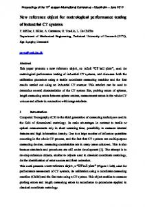
Chapter 1
Introduction This chapter will give an overview of some of the current trends in optical communication and also introduce the main topics of this thesis. The first trend which is described is the high-speed trend which aims at increasing the overall capacity of fibre optic networks. The second trend which is described is the ”revival” of optical coherent receiver structures in order to realize linear optical links for transport of wireless signals to and from antenna base stations.
1.1
High-speed trends in optical communication
The ability of optical fibre communication systems to provide high capacity has had a huge impact on the telecommunication industry and on our lives. The deployment of erbium-doped fibre amplifiers in the early 1990s, the rapid development in high-speed integrated electronic and wavelength division multiplexing has enabled high-capacity telecommunication networks and taken us with the speed of light into the information age. Even though the optical communication industry has suffered from over-capacity and lack of investment until recently, the optimism is slowly coming back. The never-ending introduction of new broadband services (high-definition TV, interactive TV, intranet, internet TV, IP telephony etc.) has resulted in a growth of the total data traffic and this demand on bandwidth is expected to continue to increase at exponential growth rates [1]. Furthermore, the deployment of fibre-to-the-customer premises, aiming at providing high bandwidth to access nodes at homes, buildings and street cabinets, has started and is now progressing fast. The projected number of homes that will be physically connected with a fibre connection is growing and is es1
timated to approach 70 million worldwide by 2010 [1]. This will have a big impact on the overall capacity of global fibre-optic networks. In addition, convergence between fixed and wireless broadband access networks is an inevitable reality – customers want access to the same applications whatever the device (fixed or mobile) and anytime. It is predicted that the number of mobile broadband subscribers is growing at a fast pace and by 2010 that number will reach 170 million [2]. This too will add extra load on the overall capacity. Moreover, a deployment of ultra-high speed data buses for connecting processor elements and shared, memories thus reducing the number of input-output back-plane connectors has also been suggested [3, 4]. With the evolution of the telecommunication sector, the nature of data traffic has moved from voice oriented to IP (Internet Protocol) oriented. The projected data traffic annual growth rates are 8% for voice, 34% for transaction data and 157% for IP traffic [1]. Based on actual data the growth of total traffic is 22/45% in 2006 according to low/high estimates [1]. However, these low/high estimates correspond to average traffic as opposed to peak traffic which is typically 50% greater. Taking the high growth scenario into account, the available capacity of installed fibres will be used up by the year 2015 [1]. In order to avoid this unwanted scenario and keep up with the increase in data traffic, a capacity upgrade for future fibre optic communication system is imperative. In today’s fibre-optic networks, the most common way of increasing the capacity is achieved by a combination of Wavelength Division Multiplexing (WDM) and Electrical Time Division Multiplexing (ETDM). In WDM systems, multiple optical carriers at different wavelengths are modulated using ETDM. In ETDM systems, a data signal is electrically multiplexed in time domain from low-speed channels to provide high-speed serial data. Today, optical transmission systems are typically running at the aggregate bit-rate of 2.5 Gb/s and 10 Gb/s per channel. However, optical communication systems at the aggregate bit-rate of 40 Gb/s per channel are commercially available and are being installed [5]. The combination of WDM and TDM technologies can significantly increase the overall capacity of fibre-optic networks. A recent experiment resulted in a new world record by demonstrating transmission of 25.6 Tb/s over 240 km [6]. This was achieved by wavelength division multiplexing of 160 channels on a 50 GHz spacing grid in the C+L bands. Each channel contained two polarization-multiplexed 85.4 Gb/s signals. For such high ca2
pacity optical communication systems, consisting of many optical channels, the optical amplifiers (Erbium Doped Fibre Amplifier (EDFA) and Raman amplifier) are critical technologies to enable long-haul transmission. We should therefore mention a transmission experiment where the total capacity of 20.4 Tb/s (204 channels × 111 Gb/s) was achieved over 240 km (3 × 80 km) using 10.2 THz inline hybrid Raman/EDFA and high-gain bidirectional distributed Raman amplification [7]. These world-record experiments demonstrate the potential of WDM and optical technologies to significantly increase the overall system capacity of fibre-optic networks. In addition, due to the demand for higher-data capacities, the race to increase single channel bit-rate has once again started to attract considerable attention from the industry and universities alike. In the last few years, there has been a lot of work on 100 Gb/s single channel ETDM communication systems, (see [8–11] and a review paper [12]). Sub-system components, essential for the operation of 100 Gb/s optical communication systems, such as a Trans-Impedance Amplifier (TIA), a baseband amplifier, a multiplexer, frequency dividers and demultiplexers, operating at 100 Gb/s, have all been demonstrated [11, 12]. Moreover, an 165 Gb/s integrated ETDM multiplexer has been very recently demonstrated in InP Double Heterojunction Bipolar Transistor (DHBT) technology, pushing the state-of-the-art in electronic circuit design [13]. However, one of the remaining challenges for the ETDM transmission systems is clock and data recovery. So far, the highest data rate at which an integrated clock and data recovery circuit has been demonstrated is 80 Gb/s, and was realized in InP DHBT technology [14]. It should however also be mentioned that a phase-locked loop based electrical clock recovery operating at 100 Gb/s has been demonstrated using off-the-self bulk components [15]. In reference [10], an integrated phaselocked loop based clock recovery for ETDM systems operating at 107 Gb/s has recently been demonstrated. However, error-free demultiplexing has not been achieved using the recovered clock signal. Demonstrating an integrated clock recovery for 100 Gb/s ETDM systems which can provide error free demultiplexing still remains a major challenge. Even though ETDM systems are under rapid development, the most practical and effective way to realize ultra-high speed single channel optical transmission systems is still to use Optical Time Division Multiplexing (OTDM). In OTDM systems, each channel is modulated onto a train of short optical pulses, all at the same wavelength. The channels are then multiplexed into a high speed OTDM data signal by bit-interleaving the modulated pulse-trains, and subsequently transmitted through a fibre link. 3
After transmission, the data signal at the aggregate bit-rate is optically demultiplexed to extract the single channels at the lower ETDM bit-rate. For a detailed description of OTDM systems, see section 1.1.1. OTDM systems can be used to generate single channel data systems up to 640 Gb/s and beyond [16–20]. The highest reported single channel bit-rate based on OTDM is 2.56 Tb/s [20]. In addition, 1.28 Tb/s single channel bit-rate experiments should also be mentioned [21, 22]. This certainly shows the potential of using the OTDM technique to increase the single channel bit-rate. However, one of the challenges associated with such highspeed OTDM systems is clock extraction and demultiplexing. Successful demultiplexing from 640 Gb/s to 10 Gb/s has been performed using fibrebased switches [16–19]. Fibre-based optical switches are promising due to their ultra-fast response. The highest bit-rate from which a clock has been extracted from in an OTDM system is 400 Gb/s using an optoelectronic phase-locked loop made from bulk components [23]. However, the extracted clock from the 400 Gb/s OTDM data signal was not used in a transmission experiment, so the quality and the performance of the recovered clock could not be evaluated. Clock extraction from high-speed data signals is a non trivial task since phase noise (timing jitter) requirements become more demanding as the data signal bit-rate is increased. This has a significant impact on the design of the clock recovery circuit. Therefore, many challenges associated with clock extraction in high-speed OTDM optical communication systems still remain to be solved and investigated. Moreover, a comprehensive theoretical framework to describe clock extraction in OTDM systems has been missing. In this thesis, we focus on OTDM optical communication systems with special emphasis on optoelectronic phase-locked loop for clock extraction, data signal regeneration and demultiplexing. In general terms, the effect of signal timing jitter on clock recovery, regeneration and demultiplexing is investigated thoroughly. A detailed theoretical analysis of a clock recovery scheme based on an optoelectronic phase-locked loop is presented. The analysis emphasizes the phase noise performance, taking into account the noise of the input data signal, the local Voltage Controlled Oscillator (VCO) and the laser employed in the loop. The effects of loop delay time and the laser transfer function are included in the stochastic differential equations describing the system and a detailed timing jitter analysis of this type of optoelectronic clock recovery for high-speed OTDM systems is performed. The impact 4
Ch. 1
Rx 1
τ Channel 1 2 3 ...N
Ch. 2
Rx 2
Pulse source
3R
Demux
Inline CR
Pre-scaled CR
Nτ
10 GHz or 40 GHz
Ch. N
Rx N
Figure 1.1: Basic OTDM system for point-to-point transmission. τ : delay, N : number of channels (integer), 3R: signal regenerator.
of the loop length on the clock signal jitter is furthermore investigated. We investigate numerically the timing jitter requirements for the combined electrical/optical local oscillators, in order for the recovered clock signal to have less jitter than that of the input signal. In addition, a novel scheme for optical clock extraction based on an optoelectronic phase-locked loop is presented and demonstrated at 320 Gb/s. Thereafter, the focus is shifted toward optical regeneration (retiming) in the presence of optoelectronic phase-locked loop based clock recovery. We analytically model the regenerator as an Ornstein-Uhlenbeck process and we end up with an analytical expression for the power spectral density of the retimed OTDM data signal [24]. The effects of OTDM data signal jitter, pulse shape, recovered clock jitter and pulse width on the jitter of the retimed OTDM data signal are investigated. For the optical demultiplexer, the impact of control signal timing jitter on a 160 Gb/s demultiplexer is investigated. This is achieved by using two different pulse sources with different noise properties. Furthermore, we investigate the interplay between the control signal pulse width and timing jitter to achieve error-free performance of the system.
1.1.1
OTDM system description
A schematic drawing of an OTDM system is shown in Figure 1.1. The considered OTDM system can be divided into the following subsystems: a transmitter, a transmission link (including a regenerator) and a receiver. At the transmitter, an optical pulse source produces short optical pulses with a repetition frequency, fbase , at the base rate (e.g. 10 GHz or 40 GHz). In particular, the following pulse sources have been used for experimental demon5
stration of OTDM systems: the semiconductor mode-locked laser [41], the mode-locked fibre-ring laser [42], the solid state mode-locked Erbium Glass Oscillator Pulse Generating Laser [43] and the electro-absorbtion modulators [44]. It has been shown that the pulse width (full-width-half-maximum) of the optical pulse source needs to be less than 40% of the bit slot of the OTDM signal [45]. Furthermore, for the fbase of 40 GHz, the pulses are required to have a pulse-tail-extinction-ratio (PTER) of 27 dB, 33 dB and 37 dB for OTDM signal bit-rates of 160 Gb/s, 320 Gb/s and 640 Gb/s, respectively [45]. Another important issue of the pulse sources is chirp and timing jitter. Ideally, it is desirable to have transform limited pulses resulting in the narrowest spectrum, i.e. the chirp is zero. The pulse source should avoid having too much of timing jitter since it may result in inter-channel interference of the OTDM signal. It has been shown that the integrated 1 timing jitter of the pulse source needs to be less that 12 of the OTDM signal −9 time slot in order to obtain a BER of 10 [46]. Following Figure 1.1, we observe that the optical pulse train is split and data modulated, at the base rate, to give N individual Return to Zero (RZ) channels, where N is an integer. Mach-Zehnder or electro-absorbtion modulators can be used to impose data modulation on the optical signal. The N channels are then appropriately delayed and subsequently bit-interleaved to form a high-speed OTDM signal with an aggregate bit-rate of N × fbase . The high speed OTDM data signal is then transmitted through the fibre link, including dispersion compensation. During the transmission, the highspeed OTDM data signal will experience different types of degradation, e.g. amplified spontaneous emission, non-linearities and jitter. It is therefore necessary to regenerate the degraded OTDM data signal and thereby extend the transmission span. Signal regeneration can be performed using all optical regeneration schemes. Using the all-optical regeneration, optical-electrical-optical conversion is avoided. The all optical signal regeneration can be performed using semiconductor-optical-amplifiers in a Mach-Zender interferometer configuration [47–49], electro-absorption modulators [50–52], non-linear optical loop mirrors [53], self-phase-modulation in highly non-linear optical fibres [54] or a Kerr switch in highly non-linear optical fibre [55]. Due to the ultra-fast response of optical fibres and semiconductor components, all-optical regeneration has great potential for high speed OTDM signals. Using a Kerr switch in optical fibres, all-optical regeneration up to 160 Gb/s has been demonstrated [55]. At the receiver, the data signal is actively demultiplexed to a frequency 6
of the base rate, which is accessible by electronic processing. Demultiplexing has been demonstrated using semiconductor [56–58] or fibre-based solutions [16–19]. Using fibre-based demultiplexers, optical demultiplexing from 640 Gb/s to 10 Gb/s has been performed [17–19]. Moreover, optical demultiplexing from 320 Gb/s to 40 Gb/s has been demonstrated using semiconductor components [56]. In order to perform all optical signal regeneration and demultiplexing, a clock recovery unit is needed. For retiming purposes, a clock signal at the line rate of the OTDM data signal is needed and the recovered clock must then have less jitter than the degraded data signal [59]. For demultiplexing purposes, a recovered clock signal at the base rate is needed, i.e. so called pre-scaled clock recovery. In order to obtain an error free demultiplexing operation (BER=10−9 ), the integrated recovered clock jitter needs to satisfy the following relation [46]: 2 ≤ τclk,jitt
q
2 (2/n)2 − τsig,jitt
(1.1)
2 where τsig,jitt is the integrated jitter of the OTDM data signal which is to be demultiplexed. n = 1 for 40 Gb/s, n = 2 for 80 Gb/s and n = 4 for 160 Gb/s. Clock recovery in OTDM transmission systems can be performed using all-optical filtering [60,61], injection locking of mode-locked fibre/semiconductor lasers or electro-absorbtion modulators [62]- [67], and optoelectronic phase-locked loops [68]- [78].
1.2
Linear photonic RF front-end trends
Due to the convergence of wireless and fixed fibre optic networks, transmission of wireless signals over optical fibres is currently receiving a lot of attention. Typically, fibre-optic networks combine wireless and fixed signal transport infrastructure by using optical fibres to connect antenna base stations with the central office [25]. Driven by the increasing capacity in fixed fibre optic networks, future wireless communication systems aim at supporting applications which require high capacity, e.g. wireless video distribution systems, wireless controlled tele-surgery, airborne radar surveillance for environmental applications, all-weather landing systems, wireless point-to-point links for disaster recovery and broadband wireless access networks. In order to satisfy these high-capacity demands, wireless communication systems will move towards 7
higher carrier frequencies ( [25,26] and references therein). The millimeterwave band (30 GHz – 300 GHz) has therefore recently attracted considerable attention and research. The future applications mentioned above are also expected to require receivers that can accommodate different ranges of the received power level of the employed radio frequencies (RF), i.e. higher dynamic range ( [27, 28] and references therein). The ability to handle higher dynamic range translates into higher system capacity and therefore better economy. In general, the optical link, connecting the antenna base station and the central office, must exhibit large bandwidth, low noise and high dynamic range in order to preserve the benefits of higher carrier frequencies. The future goal, towards which many research groups are working, is therefore high performance transport of high-frequency wireless signals to and from antenna base stations over optical fibre links (radioover-fibre links). However, moving towards higher carrier frequencies and at the same time requiring high dynamic range is very challenging, and many systems issues remain to be investigated and solved. Most techniques for encoding a wireless signal onto an optical carrier use intensity modulation which typically results in a non-linear modulation that significantly limits the dynamic range. However, optical phase modulation for transmission of wireless signals from the antenna base station has recently attracted a lot of attention due to the linear response of conventional optical phase modulators [29]- [37]. The phase modulation thus has no fundamental limit on the dynamic range. This aspect also tends to improve the noise figure and link gain since higher power levels of the wireless RF signals can be tolerated [36, 38]. In addition, the operational frequency of optical phase modulators can be extended to about the 100 GHz range [39]. In phase-modulated optical links, the wireless signal at the antenna base station is thus encoded on the phase of the optical carrier and then transmitted to the central office via fixed fibre infrastructure. However, the challenge is now moved to the receiver side. A traditional phase demodulator based on optical interference (coherent receiver) has a sinusoidal response and thus limits the dynamic range of a phase modulated link. The advantages of linear phase modulation are thereby lost. The challenge to implement a linear phase modulated link lies in the receiver structure. A few methods have recently been demonstrated to realize a linear coherent receiver either by using phase-locked loop [29]- [35] or post-detection digital-signal-processing [36, 37]. So far, the highest operational frequency a linear coherent receiver has achieved is 1.45 GHz, using a broadband optical phase-lock loop [40]. The achieved dynamic range was 113 dB·Hz2/3 8
in 1 Hz bandwidth. In this thesis, focus is on a novel linear phase-locked coherent receiver with feedback and sampling for a phase modulated optical link. The aim is to achieve a dynamic range of 90 dB·Hz2/3 in a 500 MHz bandwidth at carrier frequencies exceeding 1 GHz. A new time-domain numerical model of the phase-locked coherent receiver with feedback and sampling is developed, and the model is compared to experimental results. Using the numerical model, a detailed analysis is presented. We investigate how loop gain, tracking phase-modulator nonlinearities and amplitude modulation influence the signal-to-intermodulation ratio of the demodulated signal. Furthermore, we propose a novel method to cancel out non-linearities associated with the tracking phase modulator in the receiver and inherent non-linear response of the balanced receiver. The proposed cancellation technique is investigated in terms of input (wireless) signal power and frequency. In addition, the effects of amplitude and timing jitter of the optical pulse source on the signal-to-noise ratio of the demodulated signal are investigated. Experimental results, for two-tone measurement, using the optical phase-locked coherent receiver with feedback and optical sampling are furthermore presented.
1.3
Main contributions of the thesis
Theoretical investigations and modelling of the PLLs including noise is important in order to understand the limitations and improve the properties of circuits based on phase-locking. A large amount of literature is available on this topic, see references [80, 94]. Possibly, the most general and rigorous treatment of the topic is that of Mehrotra . However, compared to electrical PLLs treated by Mehrotra in [94], the loop length of an optoelectronic PLL used for clock extraction in OTDM systems is longer and therefore the effect of time delay on the timing jitter of the recovered clock signal must be determined. Furthermore, in an optoelectronic PLL used in OTDM systems there are two oscillators, an electrical VCO and an optical clock generating laser, the timing jitter of the extracted clock signal will thereby be influenced by the phase noise of both oscillators. The phase noise of the recovered clock signal is filtered by the laser transfer function, with a characteristic knee frequency, fch , and thus this feature must also be included in the model equations. In addition, useful OTDM clock extraction optimization tools with emphasis on the timing jitter have not been 9
reported so far. In this thesis, a detailed model of a clock recovery scheme based on an optoelectronic phase-locked loop taking into account the noise of the input data signal, the local Voltage Controlled Oscillator (VCO) and the laser employed in the loop is developed. The effects of loop time delay and the laser transfer function are also included in the model. We compute novel analytical expressions for correlation functions of the recovered clock signals. Using the correlation functions, analytical expressions for power spectral density and probability density function of the recovered clock signal are computed. Furthermore, a novel analytical expression for power spectral density of regenerated data signal, in the presence of clock recovery, is computed. Using the expressions, the timing jitter of the recovered optical clock, electrical clock and regenerated data signal is calculated, optimized and compared. A novel phase-locked receiver with feedback and sampling for linear optical phase demodulation is presented. This thesis provides first detailed analysis and deeper understanding of the proposed phase-locked receiver. In addition, we report on a novel cancellation technique, for reducing the nonlinearity associated with the tracking phase-modulator in the phase-locked receiver with feedback and sampling for phase modulated analog optical links. A review of different linearization (cancellation) techniques can be found in reference [137]. So far, linearization techniques have been applied to intensity modulated analog optical links and mostly concentrated on the transmitter side. In many cases, the linearizer circuit was design to cancel either quadratic or cubic nonlinearity and cancellation of nonlinearities occurred in relatively narrow band (input RF signal power and frequency) [137]. We show that we can simultaneously cancel nonlinearities associated with the balanced receiver and tracking LO phase modulator by purely adjusting the loop gain and tailoring the nonlinearities of the tracking LO phase modulator. No extra circuitry is needed in order to obtain the cancellation. The proposed cancellation technique is frequency and power independent and has not been reported previously.
1.4
Structure of the thesis
The thesis is organized as follows: Chapter 2 to 4 deal with phase noise, clock recovery and optical regeneration with a special focus on timing jitter. 10
Chapter 5 presents a novel phase-locked coherent receiver with feedback and sampling for optical phase demodulation. All chapters are aimed at being self-contained and can be read independently of each other. Chapter 2 deals with the effects of amplitude and phase noise on the power spectral density of a signal. A novel analytical expression for the power spectral density of a signal with amplitude and phase noise is derived. Furthermore, general stochastic differential equations are briefly reviewed. Analytical and numerical solutions of stochastic differential equations are also presented. Chapter 3 deals with clock recovery for optical communication systems. A detailed theoretical model of a phase-locked loop clock recovery is developed and presented. Using the model the effects of signal timing jitter, loop gain, time delay on the recovered clock signal are determined. Furthermore, experimental results for 320 Gb/s clock recovery. Chapter 4 deals with optical signal regeneration and demultiplexing. An analytical expression for the power spectral density of the regenerated clock signal is derived and the effects of signal timing jitter, pulse shape and pulse width on the regenerator performance are investigated at 160 Gb/s. Furthermore, the effects of timing jitter on a 160 Gb/s NOLM based demultiplexer are experimentally investigated. We also experimentally investigate how the impact of timing jitter on the NOLM based demultiplexer can be reduced. Chapter 5 deals with a novel phase-locked coherent optical phase demodulator with feedback and sampling. A time domain numerical model is developed and the performance of the demodulator with feedback and sampling is investigated in terms of loop gain, tracking phase modulator, input signal frequency and power, amplitude and timing jitter noise of the optical pulse source. Furthermore, experimental results for the phase-locked coherent demodulator with feedback and sampling are presented. The entire work presented in Chapter 5 was performed at the University of California, Santa Barbara, (UCSB) in close collaboration with Prof. John E. Bowers, Leif A. Johansson, Hsu-Feng Chou and Anand Ramaswamy and Prof. Mark Rodwell. Chapter 6 summarizes the main achievements and conclusions of the thesis.
11
12
Chapter 2
Noise Sources in Oscillators and Langevin Equations Oscillators are an integral part of many electronic and optical systems, and constitute a main part of phase-locked loops. There is therefore wide range of applications where oscillators are used, e.g. clock generation in microprocessors, wireless and wireline communication systems. In ETDM optical communication systems, oscillators are used at the transmitter, regenerator and receiver to provide synchronization. In wireless communications systems, oscillators are used for frequency translation and channel selection. In this chapter, a brief review of oscillator fundamentals and noise is given. The effect of amplitude and phase noise on the signal power spectral density is introduced and mathematically described. The combined effect of amplitude and phase noise on the power spectral density of a signal is illustrated with some numerical examples and compared to a measured power spectral density of an oscillator. Stochastic differential equations (Langevin equations) describing systems with noise are also briefly reviewed. The associated system of stochastic differential equations describing the Ornstein-Uhlenbeck process, obtained by linearization of Langevin equations, is solved using Fourier techniques and we derive novel analytical expressions for the correlation functions. Moreover, a numerical scheme for solution of stochastic differential equations is presented and demonstrated. The theory and results derived in this chapter are general and constitute a backbone for Chapter 3, 4 and 5. 13
2.1
Oscillator fundamentals
Oscillators produce a periodic output in the form of voltage. In simple terms, an oscillator can be considered as a unity-gain negative feedback amplifier [79]. A schematic of an oscillator is shown in Figure 2.1. V in
+
H(s)
V out
Figure 2.1: A schematic of an oscillator circuit. H(s) is a transfer function of the amplifier. The Figure is taken from reference [79].
The closed loop transfer function, G(s), of an oscillator circuit shown in Figure 2.1 is expressed as [79]: G(s) =
H(s) Vout (s) = Vin (s) 1 + H(s)
(2.1)
where s = jω and ω is angular frequency. Vin (s) and Vout (s) are Laplace transformation of input and output signal, respectively. and H(s) is the transfer function of the amplifier. In order for oscillation to occur at frequency ω = ω0 , the transfer function of the amplifier H(jω0 ) needs to equal -1 (the closed loop gain G(jω0 ) will thereby approaches infinity). This condition can be satisfied if ∠H(jω0 ) = π and |H(jω0 )| = 1. However, in order for the oscillation to begin and to be sustained, the loop gain of the negative feedback circuit needs to satisfy the following equations [79]:
|H(jω0 )| ≥ 1
∠H(jω0 ) = π
(2.2) (2.3)
Oscillators can be realized using Complementary Metal Oxide Semiconductor (CMOS) and Indium Phosphide (InP) technologies. Typically, the output of an oscillator is accompanied by noise. The oscillator noise is a very important design parameter which may effect the overall system performance where oscillators are involve. The description of oscillator noise and its impact on the power spectral density is addressed in the next sections. 14
2.2
Properties of phase noise in oscillators
In this section, a brief description of oscillator phase noise and its spectral characteristics are given. Important requirements for a good oscillator design include [80]: • Low phase noise • Frequency accuracy • Wide tuning range • Tuning linearity • Low power consumption • Small size • Integration on chip All these parameters are important, however, as the data rate of optical communication systems is being pushed higher and higher, phase noise becomes an important system design parameter. This is because as the data rate is increased, the requirements on oscillator phase noise become more stringent [79]. In optical communication systems, uncertainties in switching instants caused by oscillator phase noise lead to synchronization problems and this may lead to increased bit-error-rate. Apart from phase noise, oscillators usually also exhibit amplitude noise. However, for electrical oscillators the effect of amplitude noise can be significantly reduced by using an amplitude-control mechanism that largely suppresses amplitude fluctuations. In most practical cases, the effects of phase noise overshadow by far the effects of amplitude noise for the electrical oscillators. Phase noise can be described in the time or frequency domain. However, from a practical point of view, the frequency domain description of phase noise is preferable. Usually, the phase noise of an oscillator is characterized from the measurement of power spectral density. Numerous measurements have shown consistently that the power spectral density of the phase noise tends to be well approximated by [80]: W (ω) ≈
h4 h3 h2 h1 + 3+ 2+ + h0 4 ω ω ω ω 15
(2.4)
No phase noise
-30 dB/decade
Powerspectrumdenstyi
10log[W(ω)]
-40 dB/decade
-20 dB/decade
Moderate phase noise
-10 dB/decade Larger phase noise
log[ω]
(a)
(b)
Figure 2.2: (a) Typical power spectral density of an oscillator phase noise. (b) Power spectrum density of an oscillator for increasing values of phase noise. where ω is angular frequency and hv are coefficients that are particular to each individual device. In Figure 2.2(a), log[W (ω)] versus log[ω] is plotted as connected straight line segments. Each segment is labelled with the log-log slope in dB/decade. The 1/ω 4 contribution appears well below 1 Hz and it is normally not an issue for oscillators in phase-locked loops [80]. We are therefore not going to consider h4 /ω 4 term in this report. The other terms are significant. Each term arises from a different source of phase noise. The phase noise terms h3 /ω 3 and h2 /ω 2 arise from flicker1 and white noise perturbations in the oscillator. The 1/ω 3 and 1/ω 2 noise spectral components are especially prevalent in electrical oscillators. The effect of different (frequency) noise terms on system performance is dependent on the application, where the oscillators are involved. The number of publications on phase noise analysis exploded in the 1990s as the phase noise was becoming better recognized as a critical source of system degradation. Moreover, mathematical sophistication has advanced in the engineering community and advanced circuit analysis has been widely deployed to analyze the effects of phase noise. Notable publications include [81]- [92]. The two main (competing) approaches for oscillator phase noise analysis are based on Impulse Sensitivity Function (ISF) [81] and Nonlinear Stochastic Differential Equations (NSDE) [89]. Briefly described, the 1
Noise with 1/ω frequency dependence is called flicker noise.
16
ISF approach quantifies the phase disturbances caused by a noise impulse originating from a specific location in the oscillator circuit at a particular instant in the oscillation cycle. The ISF approach therefore provides information regarding the transformation of additive white and flicker noise into phase noise. An effective ISF is defined with regard to each noise source within the oscillator. The ISF method is applicable to all categories of oscillators: linear or non-linear, resonator-based or not. For a more detailed explanation of ISF approach, see [81]. The phase noise analysis presented in [89] is a non-linear analysis applicable to any oscillator that can be described by stochastic non-linear differential equations. In reference [89], the phase noise is modelled as a stochastic process and shows good agreement with experimental observations. The main outcome of the analysis presented in [89] is the power spectral density of the oscillator in the presence of phase noise. It has been shown that if the spectrum of the additive noise in the oscillator is white, the power spectral density of the oscillator has a Lorentzian shape, i.e. 1/ω 2 dependence. In this work, the approach presented in [89] is adopted for phase noise description, moreover, we also treat the systems with noise using the techniques from stochastic calculus. In the following, mathematical description of an oscillator output with phase noise is given. In the absence of phase noise, the output of an oscillator can be expressed in Fourier series as follows: g(t) = a0 +
∞ X
ai sin[iω0 t]
(2.5)
i=1
where ai are (real) Fourier coefficients and ω0 = 2πf0 . f0 is the repetition frequency and i is an integer. If g(t) is Fourier transformed, the power spectral density will contain discrete lines, i.e. delta functions at frequencies ω = iω0 . In the presence of phase noise, which we denote α(t), the signal g(t) becomes g(t + α(t)) and is expressed in a Fourier series as: g(t + α(t)) = a0 +
∞ X
ai sin[iω0 t + iω0 α(t)]
(2.6)
i=1
The effect of phase noise α(t) on a signal g(t) is to create deviations or jitter in the repetition frequency, f0 . In other words α(t) will cause spectral dispersion of a signal g(t) and this is illustrated in Figure 2.2(b). Small amounts of phase noise cause small spreading and larger amounts of phase noise cause greater spreading as illustrated in Figure 2.2(b). A randomly 17
fluctuating phase noise, α(t), can be asymptotically described as a modulated Wiener (stochastic) process [90]: α(t) =
√
c B(t) =⇒
dα √ = c Γ(t) dt
(2.7)
where B(t) is described by a 1-D Brownian motion process [93] and c is a constant determining the amount of phase noise associated with the signal and the resulting spectral spreading. We recall that Wiener process is the limiting form of the random walk as time step approaches zero [93]. The constant c will depend on the type and design of the particular oscillator and it can be related to the circuit parameters as shown in references [89,90,94]. Γ(t) is a stochastic Langevin noise force which is Gaussian distributed and is fully characterized by its ensemble mean value and correlation function:
< Γ(t)Γ(t′ ) >= δ(t − t′ )
� Γ(t) = 0
(2.8)
Using equations (2.7) and (2.8) the phase noise can be statistically characterized [95]:
� α(t) = 0
� |α(t) − α(t′ )|2 = c|t − t′ |
(2.9)
The ensemble average of the phase noise is thereby zero and its mean square value increases linearly with time. The autocorrelation function of g(t + α(t)) as t → ∞ is given by [89]: Rg,g (t, τ ) = = =
� g(t + α(t))g∗ (t + τ + α(t + τ )) ∞ X
� ak a∗i ej(k−i)ω0 t e−jiω0 τ ejω0 (kα(t)−iα(t+τ )) for t −→ ∞
k,i=−∞ ∞ X i=−∞
1
2 2 c|τ |
|ai |2 e−jiω0 τ e− 2 ω0 i
(2.10)
For practical applications, we are interested in obtaining the power spectral density of the signal g(t + α(t)). The single-sided power spectral density of a signal g(t + α(t)) is obtained by Fourier transformation of equation (2.10) [89]: G(ω) =
∞ X
|ai |2 ω02 i2 c2 1 4 4 2 ω i c + (ω + iω0 )2 i=−∞ 4 0 18
(2.11)
-40
-90 SSCR [dBc/Hz]
SSCR [dBc/Hz]
-80
-22
c=10 s -24 c=10 s -26 c=10 s
0
-80 -120 -160 -200 -240 0 1 2 3 4 5 6 7 8 9 10 10 10 10 10 10 10 10 10 10 10 10 ω [rad/s]
(a)
-100 -110 -120 -130 -140 4
10
10
5
6
10
7
10 ω [rad/s]
8
10
(b)
Figure 2.3: (a) Simulation results for the SSCR of a 10 GHz oscillator with phase noise for selected values of the constant c defined in equation (2.7). (b) Measured SSCR of a 10 GHz oscillator. Equation (2.11) shows that the power spectral density of the signal with phase noise described as Brownian motion phase error will have a Lorentzian spectrum. This is a direct consequence of the driving term Γ(t) having a constant power spectral density (white density). Usually, we are interested in the power spectral density of the oscillator, G(ω), around the first harmonic, i.e. ω0 . In practice, the Single-Sideband to Carrier Ratio (SSCR) (in dBc/Hz) is widely used to characterize the noise performance of the oscillators associated with the first harmonic. The SSCR is defined as [89]: � � G(ω0 + ω) SSCR ≡ 10 log10 (2.12) |a1 |2 where ω is the offset frequency from the first harmonic. The SSCR gives the amount of phase noise around the first harmonic. Using equation (2.12), the SSCR is shown around the first harmonic in Figure 2.3(a).
As can be seen in Figure 2.3(a), the SSCR is a straight line with a decay of 20 dB/decade which is a direct consequence of α(t) being Brownian motion phase error. It should be emphasized that by representing the phase noise as a Brownian motion phase error only the 1/ω 2 spectral component of phase noise is taken into account. The level of the SSCR curves shown in Figure 2.3(a) is fully determined by a constant c, defined in equation (2.7), and as expected the SSCR curves increase for increasing values of c. 19
9
10
In order to compare theoretical results for SSCR, obtained by using equation (2.12), with experimental results, we have measured the SSCR of an oscillator. The measured SSCR is shown in Figure 2.3(b). The experimental set-up was made by Darko Zibar and the measurement were also performed by Darko Zibar. The circuit parameters of the the oscillator were not measured. It is observed that within the frequency range 105 rad/s to 107 rad/s, the measured SSCR decreases with 20 dB/decade being in good agrement with the theoretical results. Beyond 108 rad/s there is a constant level (white noise). Moreover, below 105 rad/s, the measured SSCR curve has also a decay of 20 dB/decade, but, the curve is shifted to a lower level compared to the part of the SSCR curve in the 105 to 107 rad/s frequency range. In conclusion, the measured SSCR shown in Figure 2.3(b) is qualitatively in accordance with the theoretical SSCR curve in Figure 2.3(a) in the frequency range 105 rad/s to 107 rad/s. Outside this frequency range we do not find correlation between the theoretical and measured SSCR curves. This is because the theoretical SSCR curve only contains 1/ω 2 spectral component of phase noise.
2.2.1
Timing jitter
In the previous section, a mathematical description of a signal with phase noise has been given. In this section, we relate the phase noise of a signal to the accumulated timing jitter (time deviation). This is because, in some applications, such as clock generation, and recovery a characterization of the time deviation of signal with phase noise can be of great interest. Time deviation in the clock generation is a measure of the accuracy of the clock signal. The clock generation with large amount of time deviation may lead to system degradation, e.g. bit error rate and inter-symbol-interference. In general, the phase noise, α(t), creates deviations or jitter in the zerocrossing or transition times of the signal g(t). This is commonly referred to as timing jitter and the effect of jitter on a signal is illustrated in Figure 2.4(a). Alternatively, the deviation of each period from the ideal value can be called jitter. In addition, we have observed that the variance of phase noise, α(t), shown in equation (2.9) increases linearly with time and this means that the zerocrossings will broaden with time. Using the power density spectrum of the signal shown in equation (2.11), the timing jitter (around the first harmonic) can then be calculated using the Von der Linde method [96]: 20
5
10
4
10
3
τjitt [fs]
10
f0=10GHz f0=160GHz f0=320GHz f0=640GHz
2
10
1
10
0
10
-1
10 -30 10
Jitter
-28
10
(a)
-26
10
-24
10 c [s]
-22
10
-20
10
(b)
Figure 2.4: (a) Measured eye diagram indicting deviation of zero crossing levels due to the jitter of the signal. The Figure is a courtesy of Professor Michael Green. (b) Timing jitter as a function of a constant c for selected values of repetition frequency, f0 . Integration range: 1 Hz – f0 /2.
τjitt
1 ≡ ω0
s Z 1 ωmax G(ω0 + ω) dω π ωmin |a1 |2
(2.13)
where ωmin = 2πfmin and ωmax = 2πfmax . The fmin and fmax are the lower and upper integration limits, respectively. Inserting G(ω0 + ω) in equation (2.13) and performing the integration (MAPLE 9.5 software is used) around the first harmonic (i = 1, −1), the timing jitter of a signal having Brownian motion phase error becomes:
τjitt
√ 2 = √ πω0 � � � � � ωmax + ω0 ωmax × arctan 1 2 + arctan 1 2 2 ω0 c 2 ω0 c � � � �� ωmin ωmin + ω0 1/2 − arctan 1 2 − arctan 1 2 2 ω0 c 2 ω0 c
(2.14)
Equation (2.14) relates the phase noise of the signal to the timing jitter. Using equation (2.14), we can compute the timing jitter of a signal with phase noise as a function of the constant c for the specified integration range f = [fmin ; fmax ]. In Figure 2.4(b), timing jitter is computed as a 21
function of the constant c using equation (2.14). The repetition frequency of a signal, f0 , is varied from 10 GHz to 640 GHz and the corresponding integration range is: 1 Hz – f0 /2. As shown in Figure 2.4(b), the integrated timing jitter, τjitt , at first increases as a function of c irrespective of the repetition frequency f0 , whereafter it asymptotically reaches its final value. The final value of τjitt is dependent on the repetition frequency and the integration range in general.
2.3
Combined effect of phase and amplitude noise in oscillators
In practice, the signal may not only contain phase noise but, it may also contain amplitude noise. It is therefore essential to determine the combined effects of amplitude and phase noise on the power spectral density of a signal. In this way, we will be able to quantify the contributions associated with the amplitude and phase noise to the power spectral density of the signal, and determine which one of the effects is most detrimental for the particular system performance. The output of an oscillator in the presence of amplitude and phase noise is expressed as: f (t) = [1 + β(t)]g(t + α(t))
(2.15)
where α(t) and β(t) are assumed to be real wide-sense stationary stochastic processes with zero mean. A stochastic process
�is called � wide-sense stationary if its ensemble average is constant ( α(t) = β(t) =0) and its autocorrelation only depends on τ = t − t′ [93]: � β(t)β(t′ ) = Rβ (t − t′ ) = Rβ (τ ) (2.16) The amplitude noise β(t) is modelled as a band-limited white noise process (low-pass filtered white noise) with the power spectral density phenomenologically expressed as [97]:
� α(t)α(t′ ) = Rα (t − t′ ) = Rα (τ )
Sβ (ω) =
η [1 + (ω/ωR )2 ]
(2.17)
where ωR = 2πfR . η is low-frequency amplitude noise spectrum and fR is a roll-off frequency. In time domain, the amplitude noise, β(t), is governed by the following equation: 22
dβ β(t) η =− + Γ(t) (2.18) dt τR τR where τR = 1/ωR . The corresponding autocorrelation function of the amplitude noise, β(t), is obtained by taking the inverse Fourier transformation of equation (2.17):
� 1 Rβ,β (t, τ ) = β(t)β ∗ (t + τ ) = ηωR e−ωR |τ | ≡ σβ2 e−ωR |τ | (2.19) 2 where σβ = 12 ηωR . In practice, the amplitude and phase noise are expected to be correlated, however, for simplicity, we are going � to assume � that � the amplitude and phase noise are uncorrelated α(t)β(t) = α(t) β(t) . The autocorrelation function of the signal in the presence of amplitude and phase noise is expressed as: Rf,f (t, τ ) = =
� g(t)g∗ (t + τ )
� [1 + β(t)]g(t + α(t))[1 + β(t + τ )]g∗ (t + τ + α(t + τ ))
= Rg,g (t, τ )[1 + Rβ,β (t, τ )]
(2.20)
where Rβ,β (t, τ ) is the autocorrelation function of the amplitude noise and Rg,g (t, τ ) is the autocorrelation function of the signal with phase noise, see equation (2.10). Inserting equation (2.10) and (2.19) in (2.20), the autocorrelation function of a signal with amplitude and phase noise becomes: Rf,f (t, τ ) = +
∞ X
i=−∞ ∞ X i=−∞
1
2 2 c|τ |
|ai |2 e−jiω0 τ e− 2 ω0 i |ai |2 σβ2 e−jiω0 τ e
�
− 21 ω02 i2 c−ωR |τ |
(2.21)
The power spectral density of the signal with amplitude and phase noise is obtained by taking the Fourier transformation of equation (2.21): F (ω) =
∞ X
i=−∞
|ai |2 ω02 i2 c2 + 1 4 4 2 2 4 ω0 i c + (ω + iω0 )
σβ2 |ai |2 (ω02 i2 c + 2ωR ) (2.22) �2 1 2 2 2 ω i c + ω + (ω + iω ) R 0 2 0
Equation (2.22) relates amplitude and phase noise of a signal in frequency domain. Moreover, equation (2.22) can be used to illustrate the effects of amplitude and phase noise on the power spectral density of a signal and this is shown in next section with some numerical examples. 23
(a)
0 -20 -40 -60 -80 -100 -120 -140 -160 -180
SSCR [dBc/Hz]
SSCR [dBc/Hz]
0 Amplitude noise -20 Phase noise -40 Amp. + phase noise -60 ωR -80 -100 η -120 -140 -160 -180 -200 -220 2 3 4 5 6 7 8 9 10 10 10 10 10 10 10 10 10 10 ω [rad/s]
10
ωR
η=-90dB/Hz η=-110dB/Hz η=-130dB/Hz 2
10
3
4
10
5
10
6
7
10 10 ω [rad/s]
8
10
9
10
10 10
(b)
Figure 2.5: (a) SSCR of a signal with amplitude, phase and amplitude and phase noise. (b) SSCR of a signal with amplitude and phase noise for selected values of η.
2.3.1
Power spectrum density of a signal with amplitude and phase noise
In Figure 2.5(a), the SSCR of a signal with amplitude and phase noise is computed around the first harmonic using equation (2.22). In addition, the sole effects of amplitude and phase noise on the SSCR are illustrated as well. It is observed in Figure 2.5(a) that in the presence of phase noise only, the SSCR decays with 20 dB/decade as expected. In the presence of amplitude noise only, the SSCR contains a frequency independent level (white noise) of magnitude η and beyond ω = ωR , the SSCR curve has a decay of 20 dB/decade. In the presence of amplitude and phase noise simultaneously, the SSCR is dominated by phase noise at frequencies well below ωR and for frequencies beyond ωR , it is fully dominated by the amplitude noise. In general, we can say that for the frequency range close to the carrier, the power spectral density F (ω) is dominated by phase noise. In Figure 2.5(b), the SSCR is plotted for selected values of low-frequency amplitude noise, η, while the roll-off frequency, ωR , is held constant. For increased values of η, the SSCR becomes dominated by the amplitude noise as expected. However, for relatively low values of η = −130 dB/Hz, the SSCR is mostly dominated by phase noise. In Figure 2.6, the SSCR is computed for selected values of the roll-off frequency ωR = 2πfR while 24
SSCR [dBc/Hz]
0 -20 -40 -60 -80 -100 5 -120 ωR=2π10 rad/s -140 6 ωR=2π10 rad/s -160 7 ωR=2π10 rad/s -180 8 -200 ωR=2π10 rad/s -220 2 3 4 5 6 7 8 9 10 10 10 10 10 10 10 10 10 10 ω [rad/s]
Figure 2.6: Frequency spectrum of a signal with amplitude and phase noise for selected values of roll-off angular frequency ωR . Low-frequency amplitude noise η = −110 dB/Hz η is now held constant. It is observed that as the roll-off frequency is decreased the contribution of amplitude noise to the SSCR decreases. For relatively low values of roll-off frequency (ωR = 2 · π · 105 rad/s) the impact of amplitude noise on SSCR is negligible.
2.4
Stochastic differential equations
In sections 2.2 and 2.3, the effects of phase and amplitude noise on the power spectrum density of the signal was mathematically described and illustrated with some numerical examples. In practice, signals with noise are input to a system which then performs various operations on them, e.g. clock recovery, demodulation and analog-to-digital conversion. In addition, the system itself will have various noise sources which will add to the total noise. From a practical point of view, we would like to determine how the input signal noise is transferred to the output of the system, also taking into account the system itself may contribute with the noise. In this and the following sections, mathematical descriptions of systems driven by noisy signals are given. It is very common and convenient to describe dynamics of a systems with linear models. Among the tools for linear analysis, the Laplace and Fourier transforms are particularly valuable [98]. The related concept of a transfer function which relies on Fourier and Laplace transforms describes a transform domain relation between the input and output of a linear systems. 25
The concept of transfer functions is an extremely powerful tool and widely used by system designers. However, the concept of a transfer functions can only be applied to linear circuits. Therefore, linearization needs to be performed in order to analyze non-linear systems using the concept of transfer functions. However, this can sometimes yield erroneous results since linearization may only be valid for specific operation conditions. In the presence of a noisy signal and noise from the system itself, the method based on transfer functions can be used, however, noise sources need to be considered as additive. It has also been shown that noise generation (and frequency acquisition) in oscillators and phase-locked loops is inherently a non-linear process and linear noise techniques are not rigorously justified [89, 90, 94]. Moreover, since noise is an integral part of the oscillators output, it may lead to incorrect results to consider noise as an additive source. Instead of using transfer functions to describe the dynamics of a system, a system of ordinary differential equations can be used as an alternative approach. Moreover, if the noise sources are modelled as stochastic processes they can be easily included in the system of differential equations (stochastic differential equations). Stochastic differential equations are a more general way of describing the dynamics of the system. Furthermore, many approximations associated with the transfer functions approach are avoided by using stochastic differential equations to describe the system. However, the solution of differential equations can under certain conditions be expressed with transfer functions. Mathematical models of various electronic and optoelectronic systems, based on (stochastic) differential equations, have shown an excellent agreement with experimental results [33,89,90,94]. However, the challenge lies in solving the stochastic differential equations as explained below. In Chapter 3 and 4 of thesis, we are however going to use linearized form of stochastic differential equations. Compared to linear transfer function theory, the advantages of using linearized SDEs are limited. However, using linearized SDEs correlations functions among different noise sources and variables in the considered system can be analytically determined. This enables us to compute power spectral densities and probability density functions. The probability density functions could potentially be used to make a very accurate computations of the BERs. Furthermore, using correlations functions multiplicative noise sources (as in the case of optical regeneration) can be easily handled once the correlation functions are determined. 26
The dynamics of a time-varying system (phase-locked loop, oscillator or semiconductor laser) without any undesired perturbations can be described by a system of ordinary differential equations [95]: dx1 dt
= F1 (x1 (t), ..., xn (t)) .. .
dxn dt
= Fn (x1 (t), ..., xn (t))
(2.23)
where n represents the order of the system under consideration and xn (t) represents state variables of the physical system under consideration. We are interested in the response of such system to a state-dependent perturbation (force) dn (xn )Γn (t). Γn (t) is a stochastic Langevin force with Gaussian distribution and correlation functions described in equation (2.8). The dn term determines the size of the perturbation force and may, in general, depend on the state variable xn (t). If dn is dependent on xn (t) we say that we have multiplicative noise force and if dn is not dependent on xn (t), we have an additive noise force. In the presence of a perturbation by noise, the system of differential equations shown in equation (2.23) is rewritten as: dx1 dt
= F1 (x1 (t), ..., xn (t)) +
d1j (x1 , ..., xn )Γj (t)
n X
dnj (x1 (t), ..., xn (t))Γj (t) (2.24)
j=1
.. . dxn dt
n X
= Fn (x1 (t), ..., xn (t)) +
j=1
where dnj determine the size of the perturbation force. The system of equations shown in (2.24) is a system of stochastic differential equations, so called Langevin equations. In short, Langevin equations can be written as: dX = F(X) + D(X)Γ(t) (2.25) dt where X = [x1 , ..., xn ]T , F = [F1 , ..., Fn ]T , Γ = [Γ1 , ..., Γn ] and D is a matrix containing dnj as elements. X, F and Γ are all assumed to be real vectors. In (2.25), it is assumed that the noise sources Γn (t) are not correlated and this is expressed as: 27
� Γl (t)Γk (t′ ) = δlk δ(t − t′ )
(2.26)
where δlk is the Kronecker δ-function which equals unity for l = k and vanishes otherwise. However, in practice, there will be some degree of correlation and this may be expressed as [99]: � ̺ Γn (t)Γm (t′ ) = e−|τ |/τc (2.27) τc where τ = t − t′ and ̺ is a constant. τc represents the correlation time and if it is much smaller than other time constants in the described system, it is a reasonable approximation to say that noise sources are δ-function correlated. We also note that the phase noise expressed by equation (2.7) is a special case of a one dimensional Langevin equations for x1 (t) = α(t), √ F = 0 and d1 = c. The solution of Langevin equations are by no means trivial to obtain. However, in some special cases an analytical solution of the Langevin equations is obtainable as it will be shown in section 2.4.1. Moreover, numerical integration schemes can be used to obtain solutions of Langevin equation and this is demonstrated in section 2.4.2.
2.4.1
Computation of correlation functions for Uhlenbeck process
Ornstein-
In this section, it is shown that for an Ornstein-Uhlenbeck process, which is a special case of the Langvein equations, an analytical solution can be obtained. (For a detailed explanation of Ornstein-Uhlenbeck process, see [95].) First, we derive novel expressions for cross-spectral and cross-correlation functions of an Ornstein-Uhlenbeck process, see [59]. The cross-correlation functions are later used to in Chapter 3 and 4 to compute the autocorrelation function of the recovered clock signals and the resulting power spectral density. If a small signal expansion is performed near a stationary point X0 assuming F(X0 ) = 0 then F(X) ≈ F(X0 ) − AX, where A is a constant matrix. Furthermore, if we assume that the noise drive terms dnj are independent of state variables, the Langevin equation shown in (2.25) is reduced to an Ornstein-Uhlenbeck process: dX = −AX + DΓ(t) (2.28) dt Equation (2.28) can be solved by Fourier transformation technique. Introducing the Fourier transform X(ω) of x(t) and Γ(ω) of Γ(t): 28
X(ω) =
Z
∞
Z
∞
−jωt
x(t)e
−∞
Γ(ω) =
−jωt
Γ(t)e
−∞
1 dt ⇔ x(t) = 2π
Z
∞
1 dt ⇔ Γ(t) = 2π
Z
∞
X(ω)ejωt dω
(2.29)
Γ(ω)ejωt dω
(2.30)
−∞
−∞
and applying the inverse Fourier transformation on equation (2.28), the following is obtained:
⇒
Z ∞ Z ∞ 1 1 jωt jωX(ω)e = (−AX(ω) + DΓ(ω))ejωt 2π −∞ 2π −∞ Z ∞ 1 ((A + jωI)X(ω) − DΓ(ω))ejωt = 0 (2.31) 2π −∞
where I is the unity matrix. Equation (2.31) equals zero if ((A+jωI)X(ω)− DΓ(ω)) equals zero at all time instants. The solution of (2.28) can thereby be expressed as: (A + jωI)X(ω) − DΓ(ω) = 0 =⇒ X(ω) = (A + jωI)−1 DΓ(ω) (2.32)
� Next, we want to determine the cross-correlation functions x(τ )x(0) , where we have assumed that x(t) is a wide-sense stationary
process. This� is achieved by first computing the cross-spectral densities X(ω)(X∗ (ω))T and then transforming to the time domain. However, we first need to determine the spectral properties of Langevin noise terms. According to the Wiener-Khintchine theorem, correlation properties in the frequency domain for Langevin noise are determined using the following expression [100]:
� Γ(ω)Γ∗ (ω ′ ) = 2πY (ω)δ(ω − ω ′ )
(2.33)
where Y (ω) is the power spectral density of the Langevin noise and is a equal
constant � to 1 (white noise). Now, the cross-spectral densities X(ω)(X∗ (ω))T are expressed as: S(ω) ≡ = =
X(ω)(X∗ (ω))T
�
(A + jωI)−1 DΓ(ω)[(A − jωI)−1 DΓ∗ (ω)]T
�
(A + jωI)−1 DΓ(ω)[(Γ∗ (ω))T (A − jωI)−1 D]T
= 2π(A + jωI)−1 DDT (AT − jωI)−1 29
�
(2.34)
where we have used [(A − jωI)−1 ]T = [(AT − jωI)−1 ] [101]. We want to determine the elements, slm of the matrix S(ω), where l and m are integers. Let us define unit vectors ˆ eT1 = [1 · · · 0], ˆ eT2 = [0 · · · 1 · · · 0] T and ˆ en = [0 · · · 1]. The eigenvectors Vj corresponding to the eigenvalues λj of the matrix AT satisfying; AT Vj = λj Vj . Using the eigenvectors, we define a new basis in which the unit vectors are expressed as:
ˆ ek = bk1
1 v11 1 v12 .. .
+ bk2
2 v11 2 v12 .. .
+ · · · + bkn
1 2 v1n v1n = bk1 V1 + bk2 V2 + · · · + bkn Vn
n v11 n v12 .. . n v1n
(2.35)
where k = 1, · · · , n and bk1 , . . . , bkn are constants. The coefficients slm of the matrix S(ω) can now be expressed as:
slm = ˆ eTl Sˆ em = 2π(bl1 V1T + · · · + bln VnT )(A + jωI)−1 DDT (AT − jωI)−1 (bm1 V1 + · · · + bmn Vn ) n X n X = 2πbli ViT [(A + jωI)−1 DDT ·
·
i=1 k=1 T
(A − jωI)−1 ]Vk bmk
(2.36)
where n is the order of the system, see equation (2.23). We recall that:
(AT Vj )−1 = (λj Vj )−1 ⇒ (AT Vj )−1 Vj = ⇒ (AT )−1 Vj = Furthermore, 30
1 −1 V Vj λj j
1 Vj λj
(2.37)
(AT Vj )T
=
(λj Vj )T
⇒ VjT A = λj VjT ⇒ (VjT A)−1 = (λj VjT )−1 1 ⇒ (VT )−1 A−1 = (VjT )−1 λj 1 1 ⇒ Vj (VjT )−1 A−1 = Vj (VjT )−1 ⇒ VjT A−1 = VjT λj λj (2.38) We recall that A and AT have the same eigenvalues [101], and matrices (A + jωI) and (AT − jωI) have thereby the following eigenvalues (λj + jω) and (λj − jω), respectively. We have therefore the following: ViT (A + jωI)−1 = (AT − jωI)−1 Vk =
ViT λi + jω Vk λk − jω
(2.39) (2.40)
Inserting equation (2.39) and (2.40) in equation (2.36), the following is obtained:
slm = =
n X n X 2πbli ViT DDT Vk bmk (λi + jω)(λk − jω) i=1 k=1 n X n X i=1 k=1
2πbli ViT DDT Vk bmk (λi + λk )
�
1 1 + λk − jω λi + jω
� (2.41)
In order to obtain the end result in equation (2.41), the following decomposition was used: 1 1 1 = λi + jω λk − jω λi + λk
�
1 1 + λi + jω λk − jω
�
(2.42)
Taking the inverse Fourier transformation of equation (2.41), the crosscorrelation functions are found as follows: 31
slm (τ ) = =
� xl (τ )xm (0) � n X n X bl VT DDT Vk bm i
i
k
(λi + λk )
i=1 k=1
λk τ
e
−λi τ
µ(−τ ) + e
� µ(τ ) (2.43)
where µ(·) is the unit step function. Since the matrix DDT is symmetric, we have: ViT DDT Vk = (ViT DDT Vk )T = VkT DDT Vi . When l = m, equation (2.43) can then be expressed as: � n � n X X bmi ViT DDT Vj bmj bmi ViT DDT Vi bmi + smm (τ ) = · e−λi |τ | 2λi λi + λj =
i=1 n X
j6=i,j=1
νimm e−λi |τ |
(2.44)
i=1
Furthermore, when l 6= m, slm (τ ) + sml (τ ) can be expressed as: slm (τ ) + sml (τ ) = 2
� n � n X X bli ViT DDT Vj bmj bli ViT DDT Vi bmi + 2λi λi + λj i=1
·
j6=i,j=1
e−λi |τ | = 2
n X
νilm e−λi |τ |
i=1
(2.45)
The constants bli , where l and i are integers, appearing in expressions (2.44) and (2.45) are the elements of a vector Bl and are determined by solving the following matrix equation:
Bl = V−1 ˆ el ,
V=
v11 v12 .. . v1n
v21 . . . vn1 v22 . . . vn2 .. .. . ... . v2n . . . vnn
≡
1 v11 1 v12 .. . 1 v1n
2 n v11 . . . v11 2 n v12 . . . v12 .. .. . ... . 2 n v1n . . . v1n (2.46)
where ˆ el are unit vectors. The correlation functions presented in equations (2.44) and (2.45) are used in Chapter 3 and 4 to determine the dynamics of optoelectronic phaselocked loop based clock recovery and optical regenerator. 32
2.4.2
Numerical solution of Langevin equations
In the previous section, an analytical solution for the Ornstein-Uhlenbeck process was given and the cross-correlation functions were determined. However, the Ornstein-Uhlenbeck process is based on a linearization of the Langevin equations and this approach may not always be valid. For instance, the Ornstein-Uhlenbeck process cannot capture the non-linear dynamics of the locking process of a phase-locked loop [90, 94]. Furthermore, we cannot determine the amount of noise which would bring the phaselocked loop out of a lock. It is therefore of great importance to solve the Langevin equations in their general form and thereby describe the nonlinear dynamics of the systems under consideration. In general, there is a great interest in numerical methods to solve stochastic differential equations. Extending numerical integration techniques, which are widely used for ordinary differential equations, would be of great importance. The main approach behind numerical solutions of the Langevin equations is the following. First the stochastic Langevin force needs to be simulated. Usually, a random number generator is used to produce random numbers (e.g. in MATLAB) having a Gaussian distribution. The next step would be to integrate the stochastic differential equations. At the end, an average over a large number of realizations should be taken. It is important to have a large number of realizations of long time intervals. In this section, a simple stochastic integration scheme, a so called forward Euler scheme, is employed for solving the Langevin equations (2.24) [95]. The integration is started and ended at time 0 and Tf , respectively, using the initial condition X(0) = X0 . The time interval, [0; Tf ], is divided into Nt small steps of length dt, that is: Tf , tp = pdt, p = 0, 1, 2, ..., Nt (2.47) Nt The forward Euler scheme, for the ith state variable, xi , in equation (2.24) at a point p + 1 is given by the following expression [95]: r n X 1√ (1) xi,p+1 = xi,p + Di (xp , tp )dt + dij wjp dt (2.48) 2 dt =
j=1
where n is the order of the system in shown in equation (2.24), xip is the solution at a point p and dij are noise term coefficients, see equation (2.24). (1) wjp are (numerically generated) random numbers. Di are the first order Kramers-Moyal expansion coefficients [95]: 33
1p SSCR [dBc/Hz]
α(t) [s]
500f 0 -500f -1p -2p -2p -3p 0
2n
4n
6n
8n
10n
-110 -120 -130 -140 -150 -160 -170 -180 -190 -200 -210 -220 6 10
7
10
8
10
9
10
10
10
ω [rad/s]
t [s]
(a)
(b)
Figure 2.7: (a) Five different realizations of phase noise as a function of time. (b) SSCR of a 10 GHz signal with phase noise obtained by stochastic numerical integration.
(1)
Di
= Fi (x1 (t), ..., xn (t)) +
n X n X
dkj
k=1 j=1
∂dij ∂xk
(2.49)
The random numbers wjp are distributed according to [95]: < wjp (t) >= 0
< wjp wkp′ >= δjk δpp′
(2.50)
where δij is the Kronecker delta function. The forward Euler scheme, equation (2.48), can then be used to simulate stochastic differential equations. By performing numerical integration, correlation functions can also be determined which would then be used to estimate the spectra. However, a large number of stochastic process realizations need to be taken into account in order to improve the accuracy. Nonetheless, the stochastic Euler scheme is helpful in obtaining some estimate of the solution of the Langevin equations. In Figure 2.7(a), five different realizations of phase noise, α(t), are shown. We have used the numerical scheme shown in equation (2.48) to solve the phase noise equation (2.7) and the numerical scheme is expressed as: αp+1 = αp +
√
cin wp
34
r
1√ dt 2
(2.51)
where wp are random numbers. Each of the five realizations in Figure 2.7(a) have different paths due to the stochastic nature of phase noise. However, the ensemble average taken over many realizations should go to zero. In Figure 2.7(b), the SSCR of a 10 GHz signal with a phase noise obtained by using equation (2.51) is plotted. As can be seen from Figure 2.7(b), the SSCR is a straight line with decay of 20 dB/decade which is in accordance with the theoretical and experimental results in Figure 2.3.
2.5
Summary
In this chapter, we have reviewed oscillator fundamentals and phase noise theory. Furthermore, an analytical expression for a power spectral density of a signal with amplitude and phase noise was derived. Using the analytical expression, the effects of amplitude and phase noise on the power spectral density of a signal have been quantified. We have shown that the power spectral density is dominated by phase noise around the carrier frequency. Beyond the roll-off frequency, the power spectral density of a signal is fully dominated by amplitude noise. For very small values of roll-off frequency, the effect of amplitude noise was negligible. Furthermore, we have presented Langevin equations and the corresponding Ornstein-Uhlenbeck process. We have derived analytical expressions for cross-correlation functions for the Ornstein-Uhlenbeck process and this result will be used in Chapter 3 and 4 to analyze the dynamics of clock recovery and regenerator.
35
36
Chapter 3
Clock Recovery Based on an Optoelectronic Phase-Locked Loop In digital communication systems, clock recovery is an integral part of the data-recovery section. The purpose of clock recovery is to provide information about the sampling time to the decision circuit and thereby synchronize the decision process. The output of a clock recovery circuit is a signal with a frequency inversely proportional to the bit-rate or a fraction of the bit-rate of a data signal. In this chapter, a brief review of important clock recovery parameters is at first given. Thereafter, a review of the most typical clock recovery techniques, used in optical communication systems, is presented. We also explain advantages and disadvantages of the reviewed clock recovery techniques, and we chose to focus on an Optoelectronic Phase-Locked Loop (OPLL) based clock recovery. The Langevin equations describing the optoelectronic phase-locked loop based clock recovery, with noise sources, are thereafter derived on which we base our novel numerical model. We use correlation functions derived in Chapter 2 to derive the autocorrelation functions of the recovered clock signals and compute novel analytical expressions for timing jitter. Moreover, we investigate how the phase noise, loop gain, loop filter bandwidth, time delay and laser characteristic knee frequency influence the timing jitter of the recovered clock signal. A simple experimental set-up is constructed to verify the numerical model. In addition, experimental results for clock 37
recovery operating at 320 Gb/s are presented.
3.1
Review of clock recovery parameters
Before we go into the details of different clock recovery schemes, we review important clock recovery parameters which are: • Lock-in range • Lock-in time • Hold-in range • Jitter (jitter transfer, jitter generation and jitter tolerance) The lock-in range is the range of frequencies within which an unlocked clock recovery can acquire a lock. The lock-in range should be large enough in order to accommodate any frequency drift of the data signal. Lock-in time is the time needed to obtain a lock. For applications such as packet switching very fast locking time (∼1 ps) is needed [102]. The hold-in range is the range of frequencies within which (locked) clock recovery can statically maintain phase tracking when frequency drift or other disturbances occur in the data signal. For instance, if the data signal has a relatively long range of zeros and the clock recovery is not loosing its lock, then we say that the clock recovery has a large hold-in range. Clock recovery jitter is a another very important parameter. Since the clock recovery provides sampling time for a decision circuit, it is important that the recovered clock does not have a lot of jitter. If the clock recovery has a lot of jitter then this may lead to incorrect bit identification by the decision circuit which would then result in bit-error-rate [103]. The jitter transfer function of a clock recovery circuit describes how jitter from the input signal is transferred to the jitter of the output signal (recovered clock signal). The clock recovery must follow slow frequency drifts (low frequency jitter components) in order to ensure phase tracking of the input data signal. Clock recovery should on the other hand not track fast drifts (high frequency jitter components) since this may lead to erroneous detection of the bits [79]. A typical jitter transfer function of a clock recovery circuit is shown in Figure 3.1 [79]. Figure 3.1 shows that clock recovery should exhibit low-pass characteristics. The bandwidth of the jitter transfer function corresponds to the bandwidth 38
1
A |
out
A / ni |
Jitter peaking
Jitter frequency
Figure 3.1: Typical jitter transfer function of a clock recovery [79]. The Ain is the amplitude of input jitter frequency components and Aout is the amplitude of output jitter frequency components. of the clock recovery circuit. Another characteristic of the jitter transfer function is jitter peaking. The jitter peaking is a ripple in the jitter transfer function of the clock recovery as illustrated in Figure 3.1. The bandwidth of the clock recovery and the allowed jitter peaking depends on the application where clock recovery is involved. For instance for Synchronous Optical NETwork (SONET), the jitter transfer function should have a 120 kHz bandwidth and the jitter peaking should be less than 0.1 dB [79]. Having such a low loop bandwidth is very challenging since it may compromise the stability of the clock recovery as shown in [80]. Jitter generation refers to the jitter produced by a clock recovery circuit itself when the input data has no jitter. Jitter generation is thereby dependent on how much jitter different components in the clock recovery generate. In general, jitter generation is very dependent on the clock recovery topology. Jitter tolerance specifies how much input jitter a clock recovery must tolerate without increasing the bit-error-rate. This specification is typically described by the mask function and it is shown in Figure 3.2. The mask function also exhibits a low-pass behavior which is a consequence of the jitter transfer function having a low-pass characteristics. For a satisfactory performance of the clock recovery, the jitter tolerance curve should be above the reference curve, see Figure 3.2. Once again specifications on jitter tolerance is dependent on the application where the clock recovery is involved. In general, a clock recovery should be able to tolerate large amounts of low frequency jitter while the jitter tolerance decreases as the 39
Reference Unsatisfactory performance
Jtiertoe l rance a [u . ].
Satisfactory performance
Jitter frequency
Figure 3.2: Jitter tolerance curve of a clock recovery. frequency is increased as illustrated in Figure 3.2. Since the focus of this thesis is on noise in clock recovery systems, only clock recovery parameters such as jitter generation and jitter transfer are treated. The hold-in range, lock-in range and lock-in time are thereby not treated partly because they fall out of the scope of the thesis and partly because they may require nonlinear model of clock recovery. This thesis will not cover nonlinear clock recovery models. However, for the reference on nonlinear clock recovery models see [107, 114, 123].
3.2
Review of clock recovery schemes for optical communication systems
In this section, a brief review of clock recovery schemes in optical communication systems is given. We start by considering ETDM optical communication systems. It should be mentioned that in ETDM systems, prior to clock extraction, an electro-optical conversion is performed using a photodiode in order to convert the optical data signal into electrical domain. In simple terms, clock recovery is nothing else than a bandpass filter with a high Q-value. The simplest way to perform a clock recovery in ETDM communications systems is to use an electrical bandpass filter and isolate the desired frequency component from the incoming data signal [104]. However, this approach assumes that the data signal has the desired frequency component. The advantage of this clock recovery scheme is apart from its simplicity a very fast lock-in time. Using this type of clock recovery scheme lock-in times in the range of ps can be obtained. Furthermore, if the electri40
Input
Loop filter
PC
VCO Figure 3.3: Basic phase lock loop. PC: phase comparator, VCO: voltage controlled oscillator.
cal bandpass filter is made from passive components, it is possible to obtain low jitter generation. The disadvantage of this scheme is low lock-in and hold-in range. This is because the pass-band of this type of clock recovery is pre-set and there is thereby very limited flexibility. If the data signal undergoes some frequency drift, the clock recovery may not be able to follow it and will thereby loose the lock. Another issue with this technique is how well the pass-band is designed. Any ripple in the pass-band will have an undesired effect on the jitter transfer function. Moreover, since the bandwidth is finite this may cause significant jitter transfer [105]. We would need a high Q-value in order to have a narrow bandwidth, such that the 3 dB frequency of the jitter transfer function is sufficiently low. Typically, in high-speed ETDM transmission systems, clock recovery is performed by the use of electrical phase-locked loops, see [80, 106]. Before considering the PLL based clock recovery, the basic principles of a PLL are first described. A diagram of a basic PLL is shown in Figure 3.3. A PLL synchronizes an output signal, which is locally generated in the loop, in frequency as well as in phase to an input signal. In the synchronized (locked) state the phase error between the input signal and locally generated signal is zero or very small. If the total phase error (which includes relative phase and frequency) begins to build up, the feedback mechanism acts on the local oscillator in such a way that the phase error is brought down to zero again. The loop has thereby re-obtained a lock. The PLL principally consists of three components: 1. A phase comparator (mixer). 41
2. A loop filter. 3. A Voltage Controlled Oscillator (VCO). The Phase Comparator (PC) mixes the incoming data signal with the locally generated clock signal from the VCO. The frequency content of the incoming data signal is thus mixed with the frequency content of the locally generated clock signal. Since the process of mixing corresponds to mathematical multiplication, the output of the PC is a signal which includes the phase error, i.e. the error signal, plus the signals at higher frequencies. The output of the PC is then passed through the loop filter, in order to cancel high frequency terms, and is subsequently fed back to the VCO. The output from the VCO is the (desired) recovered clock signal. The PLL based clock recovery is fully determined by its loop bandwidth which is directly proportional to the closed loop gain of the system [80]. The advantage of the PLL based clock recovery is its large lock-in and holdin range which can be tuned using the loop bandwidth. This translates into very stable operation of PLL based clock recovery. Furthermore, this type of clock recovery scheme is very flexible since the performance can be easily adjusted using the loop bandwidth. Decreasing the loop bandwidth will decrease the 3 dB frequency of the jitter transfer function. A clock recovery circuit based on a PLL can thereby provide a clock signal with low timing jitter and high stability. However, decreasing the loop bandwidth may result in peaking of jitter transfer function due to positioning of the poles and zeros of PLL transfer function. Careful attention is required to avoid this effect [80]. A disadvantage of the PLL based clock recovery is that it has relatively high lock-in time [107]. However, a lock-in time can be reduced by optimizing the loop bandwidth and it has been shown that a lock-in time as low as 15 ns is obtainable [107]. An additional issue with the PLL based clock recovery is jitter generation. Loop components such as VCO and electronics will contribute with noise which will be translated into jitter. The loop components of the PLL based clock recovery need therefore to have very low jitter, and as it will be shown later in this chapter, VCO has a significant role on the jitter generation of this type of clock recovery. Third type of electronic clock recovery scheme is injection locking of a free-running electrical oscillator [108, 109]. The main principle behind this technique is that the internal oscillator can be locked in frequency if the input data signal is applied. This approach is a mixture of band-pass filter 42
approach and a PLL based clock recovery. If the free-running oscillator has very low-noise, then the jitter performance of this type of clock recovery can be significantly improved compared to the PLL based clock recovery. In this approach there are no loop components (loop filter and amplifier) reducing the overall noise performance. The disadvantage of this type of clock recovery is its limited bandwidth. The limited bandwidth may, as mentioned earlier, translate into low lock-in and hold-in ranges. As we move away from ETDM towards high-speed OTDM transmission systems clock recovery becomes more challenging. This is partly because of the very high speeds of OTDM transmission systems and partly because the data signal has only frequency components at line rate (aggregate bit-rate). The recovered clock signal in OTDM systems can be used for either retiming or demultiplexing. For retiming purposes, clock signal at the line rate of OTDM data signal is needed. For demultiplexing purposes, a recovered clock signal at the base rate is needed, so called pre-scaled clock recovery. Recovering a base rate clock from OTDM data signal is very challenging since the OTDM data signal has no base rate frequency component. The clock recovery therefore needs to lock to the line rate of the OTDM data signal. Since the speed of the OTDM data signal can easily exceed 160 Gb/s [110] using electronics to achieve base rate clock extraction may be out of reach for now [15,111] and therefore an alternative way of performing clock recovery is desirable. Many all-optical or optoelectronic clock recovery techniques have been demonstrated for OTDM transmission systems and they are mostly based on: • All-optical filtering ( [60]- [61] and references therein). • Injection locking in mode-locked fibre/semiconductor lasers or electroabsorbtion modulators ( [62]- [67] and references therein). • Optoelectronic phase-locked loops ( [68]- [78] and references therein) The above mentioned techniques for clock recovery in OTDM systems all basically rely on modified versions of clock recovery schemes for ETDM systems. The operational principles are therefore similar to those described earlier for ETDM systems. In addition, the pros and cons described for ETDM clock recovery schemes are thereby also the same for the mentioned OTDM based clock recovery schemes. 43
For regeneration purposes, all-optical clock recovery techniques based on optical filtering and injection locking are advantageous since they provide a clock at the line rate [60]- [67]. Recently, a mode-locked semiconductor laser has been locked to a 160 Gb/s input OTDM data signal and generated 160 GHz recovered optical clock signal [65]. The recovered 160 GHz clock signal had low jitter and 3 dB bandwidth of the jitter transfer function was relatively. Also, a clock recovery based on quantum dot self-pulsating semiconductor laser was shown to provide very low jitter (190 fs) line rate clock extraction at 40 Gb/s [62]. Furthermore, it was demonstrated that this particular type of clock recovery could satisfy the ITU-T recommendations for jitter transfer function [62]. For demultiplexing operations a recovered clock at the base rate is needed. In most cases, if the clock recovery is performed using all-optical filtering or injection locking techniques, some extra processing is needed in order to obtain base rate clock signal [112]. As a result, PLL based optoelectronic clock recovery is the dominant choice for demultiplexing operations. Using an electrical PLL based clock recovery, the highest data rate from which a base rate clock has been extracted is 100 Gb/s [15]. The main bottleneck in the electrical PLL based clock recovery is the mixer and photodiode. It is very difficult to make high-frequency mixers with high frequency efficiency. An electrical mixer becomes too slow for clock extraction from OTDM systems operating above 100 Gb/s and an optoelectronic PLL must instead be used. The central component in the optoelectronic PLL is the optical mixer [23,68,75]. Non-linear optical effects can be used to achieve mixing in a Semiconductor Optical Amplifier (SOA). Non-linear effects such as Cross Gain Modulation (XGM) [75], Four Wave Mixing (FWM) [23], Cross Phase Modulation (XPM) [77] and filtering-assisted XPM [68] have been used. The advantages of using an optical mixer is that we can avoid implementing a high frequency electrical mixer and a fast photodiode, both of which are difficult to manufacture, and at the same time reach higher bit rates. The output of the optical mixer is passed through the optical bandpass filter in order to extract the modulated optical signal containing the error signal. The rest of the loop remains the same as in the electric PLL where only low-speed and simple electronics are required. The VCO is used to control the optical clock signal generating laser whose pulses are then injected into the optical mixer. The highest data bit rates from which a pre-scaled base rate clock has been extracted have been achieved with an optoelectronic PLL (400 Gb/s) [23]. In addition, pre-scaled clock extraction of a 10 GHz clock signal 44
from a 320 Gb/s data signal should also be mentioned [68, 76]. The clock extraction reported reference [68] was achieved using filtering-assisted XPM in optoelectronic PLL. The approaches based on FWM and filtering-assisted XPM therefore seem to be good candidates for applications at very high bit rates (beyond 160 Gb/s). This is because the non-linear processes such as FWM and filtering-assisted XPM can be used to achieve mixing at very high bit rates and thereby generate the error signal to control the optoelectronic PLL. It is therefore believed that the OPLL based clock recovery has a great potential for ultra-high bit rate OTDM systems. In summary, clock recovery based on an optoelectronic phase-locked loop can offer very high speed operations while maintaining all the benefits of the PLL based clock recovery. We therefore choose to concentrate on the optoelectronic PLL based clock recovery in this thesis.
3.3
Optoelectronic phase-locked loop – a brief descriptions
In this and following sections we will focus on a balanced optoelectronic PLL for clock extraction from high-speed data signals, and analyze its stability and noise properties. The block diagram of the balanced OPLL is shown in Figure 3.4. The phase comparator mixes the optical high-speed data signal (e.g. 160 Gb/s) with a locally generated optical clock signal at the base rate frequency (e.g. 10 GHz) producing an error signal. The mixing process corresponds to a mathematical multiplication with a mixer gain, G. The mixer output is a slowly varying signal proportional to the sine of the phase difference between the data and the optical clock signal. The optical error signal is then converted into the electrical domain. The balanced (low bandwidth) photodetection provides the subtraction of the DC level from the error signal, which results in a bipolar error signal. This subtraction also helps to stabilize the error signal against fluctuations in the input signal power levels. The signal is then low pass filtered and fed back to the VCO, which controls the frequency of the optical clock generating laser. In an optoelectronic PLL based clock recovery, a considerable time delay is very likely to occur, since the loop length of an OPLL is often much longer than in an electrical PLL. Time delays in an OPLL may typically arise from the presence of an Erbium Doped Fibre Amplifier (EDFA) and/or a pulse compression stage in the loop. An EDFA may 45
Attenautor
Photodetector Loop filter
PC data,α in
τd
+
φe
PI
A
α clk
Laser
αvco Recovered electrical clock
Recovered optical clock
ψe Kvco VCO
Figure 3.4: Diagram of the balanced OPLL based clock recovery. τd : the total time delay in the loop, PC: phase comparator (mixer), PI: proportional integrator, A: amplifier gain, VCO: voltage controlled oscillator, Kvco : gain of the voltage controlled oscillator, αin : input phase noise, αclk : phase noise of the laser, αvco : phase noise of the VCO, φe : phase difference between αclk and αin , and ψe : applied signal to the VCO.
also sometimes be needed to amplify the optical clock signal before the phase comparator. It has been demonstrated that intra-loop time delays destabilize the loop [113, 114]. So far, there has been a lot of experimental work on clock recovery based on an optoelectronic PLL. However, theoretical and modelling work concerning optoelectronic PLLs has been limited. Especially, as the speed of the data signal is increased noise analysis of optoelectronic PLL is of great importance. This is because, the requirements for the extracted clock signal timing jitter become more stringent, as the bit rate of the data signal is increased [46]. In general, theoretical investigations and modelling of the optoelectronic PLLs including noise are important in order to understand the limitations and improve the properties of circuits based on phase-locking. A large amount of literature, for electrical PLLs, is available on this topic, (e.g. [80, 94] and references therein). Possibly, the most general and rigorous treatment of the topic is that of Mehrotra [94]. However, compared to electrical PLLs, the loop length of an optoelectronic PLL is longer and therefore the time delay must be included in the model. Furthermore, in an optoelectronic PLL there are two oscillators, an electrical VCO and an optical clock generating laser. The timing jitter of the extracted clock signal will therefore be influenced by the phase noise of both oscillators. The 46
phase noise of the recovered clock signal is filtered by the laser transfer function, with a characteristic knee frequency, fch , and thus this feature must also be included in the model equations. In the following sections, a detailed phase noise analysis of an optoelectronic PLL based clock recovery is performed.
3.4
Derivation of Langevin equations for OPLL
In order to study the dynamical behavior of the optoelectronic PLL presented in Figure 3.4 stochastic differential equations, describing the phase error between the input data signal and the local oscillators, need to be derived. The intensity of the input data signal in the presence of phase noise, αin (t), originating from the pulse source at the transmitter, regenerators and in-line amplifiers, is expressed in Fourier series as [100]: Pin (t + αin (t)) = s0 + 2
∞ X
sk sin[2πkf0 t + 2πkf0 αin (t)]
(3.1)
k=1
where k is a positive integer. The constants s0 and sk are (real) Fourier coefficients and f0 is the frequency of the aggregate bit-rate (e.g. 40 GHz, 160 GHz, 320 GHz etc.) [115]. The input data signal phase noise, αin (t) is described by a 1-D Brownian motion stochastic process and cin is a constant determining the amount of phase noise associated with the input signal, as explained in section 2.2, equation (2.7). The intensity of a locally generated optical clock signal is similarly expressed by a Fourier series as [100]:
Pclk (t + αclk (t)) = c0 + 2
∞ X
cq cos[2πq(f0′ /m)t + 2πq(f0′ /m)αclk (t)]
q=1
(3.2)
where q is a positive integer. The constants c0 and cq are (real) Fourier coefficients. The repetition frequency of the optical clock signal is f0′ /m, where m is an integer. The frequency f0′ /m (e.g. 10 GHz or 40 GHz) corresponds to the free-running frequency of the optical clock signal generating pulse source and it is chosen so that it is close to the base rate frequency, fbase (e.g. 10 GHz, 40 GHz), of the optical input data signal [115]. αclk (t) is the phase noise of the optical clock signal and is modelled as a band-limited Brownian motion stochastic process, as later shown in equation (3.9). The 47
output of the phase comparator (mixer), see Figure 3.4, is defined to be a product between the optical clock signal in equation (3.2) and the optical data signal in equation (3.1) with a gain G. Phase comparators are frequently modelled as multipliers, partly for analytical convenience and partly because many practical phase comparators are good approximations to multipliers [80]. The optical signal after the mixing contains low frequency components as well as high frequency components, which exceed the aggregate bit-rate (> f0 ). A slow photodiode with bandwidth BW ≪ fbase is used to convert the signal from the optical to the electrical domain and is also used to filter out high frequency components. It is assumed that the responsivity of the photodiode is constant in frequency. The fundamental frequency component of the optical data signal f0 (k = 1) interacts with the m’th frequency component (q = m) of the optical clock signal, resulting in the frequency component ∆f = (f0′ − f0 ). When the aggregate bit rate of the optical data signal is 160 Gb/s and the base rate is 10 Gb/s, we have m = 16. The frequency component ∆f is smaller than the bandwidth of the photodiode and can therefore be detected and forms the fundamental frequency component. Furthermore, following Figure 3.4, it can be observed that part of the optical data signal is first attenuated, in order to match the signal powers, and then passed through the second photodiode which is identical to the first one. Since the photodiode is slow, only the DC frequency component of the optical data signal passes through. The balanced photodetection (BW in the MHz range) thereby provides a subtraction of the DC level from the error signal. After balanced photodetection the error signal, e(t), is expressed as:
e(t) =
RGs′0 c′0
+ 2RG
∞ X
si ci·m sin[iΦe (t)]
i=1
Φe (t) = ∆ωt + 2πf0′ αclk (t) − 2πf0 αin (t)
(3.3)
where i is a positive integer and R is the responsivity of the photodiode. s′0 c′0 is the remaining DC level in the error signal after the subtraction. Even though the balanced photodetection provides a subtraction of the DC levels, cancellation may not be complete due to imperfections in the electronics. In order to perform phase noise analysis of the system, the locally generated optical clock signal must be synchronized to the input data signal, 48
i.e. f0 = f0′ . We choose to operate with a normalized total phase difference, φe (t) ≡ Φe (t)/(2πf0 ). The advantage of using the normalized form of Φe (t) is that the phase noise analysis will not be affected by the frequency difference between the input signal and the locally generated clock signal. The normalized phase difference, φe (t), is given by: φe (t) = ∆ωn t + αclk (t) − αin (t)
(3.4) RGs′0 c′0
whereP∆ωn = ∆ω/(2πf0 ). The normalized error signal en (t) ≡ + ∞ 2RG i=1 si ci·m sin[iφe (t)] is now applied to the loop filter, a Proportional Integrator (PI) filter. In the time domain the output of the PI filter ψe (t) is defined as [116]: � � dψe den τ1 = A en (t) − τ2 (3.5) dt dt where A is the gain of the electrical amplifier in the loop. τ1 represents the integration time of the filter (inversely proportional to the PI filter bandwidth) and τ2 determines the DC gain of the PI filter. The reason that we concentrate on a PI loop filter, is because it is more tolerant to long loop lengths compared to the Low Pass (LP) and Active Lag (AL) filters [114]. The output signal of the VCO is written as: v(t) = V0 cos[2πf0′′ t + 2πf0′′ αvco (t)]
(3.6)
where f0′′ is the free-running frequency of the VCO, also chosen close to the base rate of the optical data signal, and V0 is the amplitude of the VCO signal. αvco (t) is the phase noise associated with the VCO. It has been shown by Mehrotra [94] that the phase noise of the oscillator in the presence of the applied signal is governed by the following stochastic differential equation: dαvco = ν T (t + αvco (t))Γp (t) + νctrl (t + αvco (t))ψe (t) (3.7) dt where Γp (t) is a vector of p uncorrelated white noise sources and ν(·) is a periodic function which depends on the noise source intensities and the response of the linearized oscillator circuit [94]. νctrl (·) is the component of ν(·) which corresponds to a unit noise source present at the control node of the VCO [94]. In order to perform noise analysis of the PLL we must assume that the loop is locked and we are therefore only interested in the asymptotic behavior of the VCO phase noise. Asymptotically, equation (3.7) reduces to [94]: 49
√ dαvco = Kvco ψe (t) + cvco Γvco (t) (3.8) dt where cvco is a constant determining the amount of phase noise associated with the free-running VCO and Kvco is the average gain of the VCO. Γvco (t) is a white noise source. From the diagram of the OPLL, Figure 3.4, we observe that the signal from the VCO is directly modulating the optical pulse source (laser). Under the assumption that the VCO and the laser are synchronized, the phase noise of the VCO, αvco (t), will be filtered by the laser transfer function, with a characteristic knee frequency of fch [117, 118]. The characteristic knee frequency, fch , denotes the bandwidth around the laser’s center frequency within which phase noise is transferred from the VCO to the laser [119]. The phase noise, αclk (t), of the laser is thus expressed as: dαclk γe (t) √ =− + cclk Γclk (t) (3.9) dt τch where τch = 1/(2πfch ) and cclk is a constant describing the magnitude of the phase noise of the free-running laser described by the white noise source Γclk (t). γe (t) is the phase noise difference between the VCO and the optical pulse source, i.e. γe (t) = αclk (t) − αvco (t). The stochastic differential equation describing the phase noise difference between the VCO and the optical pulse source is then obtained by differentiating γe (t) and using equation (3.8) and (3.9): √ √ dγe γe (t) =− − Kvco ψe (t) + cclk Γclk (t) − cvco Γvco (t) dt τch
(3.10)
The effect of a time delay, τd , see Figure 3.4, is taken into account by incorporating a delay in αclk (t) and thereby equation (3.4). Therefore, φe (t) in equation (3.4) changes to φe (t) = ∆ωn t + αclk (t − τd ) − αin (t). By using equation (3.10), the stochastic differential equation describing the total phase error in the loop is obtained by differentiating φe (t) and is expressed as: √ dφe (t) γe (t − τd ) √ = ∆ωn − + cclk Γclk (t − τd ) − cin Γin (t) (3.11) dt τch √ where dαin /dt = cin Γin (t) and Γin (t) is a white noise source associated with the input data signal. Inserting equation (3.11) in (3.5), the output from the loop filter becomes: 50
dψe dt
� � ∞ ∞ τ2 X 1 X = DC + ζi sin[iφe (t)] + ζi i cos[iφe (t)] τ1 τ1 i=1 i=1 � � √ γe (t − τd ) √ × − ∆ωn + − cclk Γclk (t − τd ) + cin Γin (t) τch (3.12)
The dynamical behavior of the optoelectronic PLL in the presence of noise ARGs′0 c′0 is governed by equations (3.10), (3.11) and (3.12) where DC = τ1 and ζi = 2ARGsi ci·m . ζi describes the overall gain in the loop. si is the ith Fourier coefficient of the input data signal in equation (3.1) and ci·m is the (i · m)th Fourier coefficient of the optical clock signal is equation (3.2).
3.5 3.5.1
Linearization of Langevin equations describing the OPLL Zero time delay
In this subsection it is assumed the time delay is set to zero, i.e. τd = 0. We want to linearize the Langevin equations, (3.10) – (3.12), by performing a small-signal expansion near a stationary point; (x, y, z) ≡ (φe , γ e , ψ e ) = 0. For convenience we introduce:
φe (t) = x ¯ + ∆x(t)
(3.13)
γe (t) = y¯ + ∆y(t)
(3.14)
ψe (t) = z¯ + ∆z(t)
(3.15)
where ∆x(·), ∆y(·) and ∆z(·) are small disturbances around the stationary points (φe , γ e , ψ e ). In order to get a dynamic response of the loop, we need to derive the differential equations describing the disturbances ∆x, ∆y and ∆z. The expressions in equations (3.13) – (3.15) are inserted in (3.10) – (3.12). After linearization, the following is obtained1 : 1
In practise s1 cm >> si ci·m for i ∈ [2; ∞], and only i = 1 is considered. This is observed by considering the pulse width requirements for the high-speed OTDM data signal [45].
51
1 ˙ 0 0 − τch ∆x ∆x ˙ 1 ∆y = 0 − τch −Kvco ∆y τ2 ζ1 ζ1 ˙ ∆z ∆z 0 τ1 τ1 τch √ √ 0 c − cin Γvco (t) √ √ clk Γclk (t) cclk 0 + − cvco τ2 ζ1 √ τ2 ζ1 √ Γin (t) 0 − τ1 cclk τ1 cin
(3.16)
To obtain the characteristic equation describing the eigen (natural) solution of the system (without the driving noise terms) we assume solutions of the form: ∆x = ∆x0 eλt , ∆y = ∆y0 eλt and ∆z = ∆z0 eλt . ∆x0 , ∆y0 and ∆z0 are amplitudes of the disturbances and λ are eigenvalues. Inserting ∆x, ∆y and ∆z in (3.16), the expression for eigenvalues, λ, can be obtained. The eigenvalues are then governed by the following characteristic equation: λ3 +
3.5.2
1 2 Kvco ζ1 τ2 ζ1 Kvco λ + λ− =0 τch τ1 τch τ1 τch
(3.17)
Non-zero time delay
In the presence of time delay, the equations describing the dynamics of the OPLL include a delay term as shown in equations (3.10) – (3.12). The delayed differential equations are harder to deal with and we would therefore like to transform the delayed differential equations into ordinary differential equations. The method which we use is described in [120] and is valid for relatively small values of the ratio τd /τch , i.e. τd /τch < 500 ns [121]. Without the driving terms caused by noise, the system of equations (3.10) – (3.12) can be written in form: ˙ = f (w) w w = [w1 (t), w2 (t), w3 (t), w4 (t)]T ≡ [φe (t), γe (t), γe (t − τd ), ψe (t)]T
(3.18)
For each of the variables in w = [w1 (t), w2 (t), w3 (t), w4 (t)]T , a first order differential equation needs to be derived in order to get the total response of the loop. The variable w3 (t) is a delayed version of w2 (t), i.e. w3 (t) = w2 (t − τd). Using the first order Pade(1,1) approximation and following the 52
procedure described in [120] and [121], a differential equation describing w3 (t) is obtained: � � dw2 2 dw3 = w2 (t) − w3 (t) − dt τd dt
(3.19)
Using equation (3.19), the differential equations in (3.10) – (3.12) are rewritten as (without the noise driving terms): dw1 dt dw2 dt dw3 dt dw4 dt
= ∆ωn −
w3 (t) τch
(3.20)
w2 (t) − Kvco w4 (t) τ � ch � 2 w2 (t) w2 (t) − w3 (t) + + Kvco w4 (t) τd τch
= −
(3.21)
=
(3.22)
= DC +
� ∞ � � � ∞ 1 X τ2 X w3 (t) ζi sin[iw1 (t)] + ζi i cos[iw1 (t)] · − ∆ωn + τ1 τ1 τch i=1
i=1
(3.23)
Next, we want to linearize the Langevin equations in (3.20) – (3.23), by performing a small signal expansion near a stationary point; (¯ x, y¯, q¯, z¯) = (w¯1 , w¯2 , w¯3 , w¯4 ) = 0. Once again, as in (3.13)-(3.15), we introduce: w1 (t) = x ¯ + ∆x(t), w2 (t) = y¯ + ∆y(t), w3 (t) = q¯ + ∆q(t), w4 (t) = z¯ + ∆z(t). After linearization and including the noise terms, the following is obtained:
˙ ∆x ˙ ∆y ˙ ∆q ˙ ∆z
=
0 0 0 ζ1 τ1
0 1 − τch 2 1 τd + τch
0
√ 0 0 cclk √ √ − cvco cclk 0 + 0 0 0 √ 0 0 − τ2τ1ζ1 cclk
53
1 − τch 0 − τ2d τ2 ζ1 τ1 τch
√ − cin 0 0 τ2 ζ1 √ cin τ1
0 −Kvco Kvco
∆x ∆y ∆q ∆z 0 Γvco (t) Γclk (t) Γclk (t − τd ) Γin (t)
(3.24)
Following the same principle as in section 3.5.1, the eigenvalues are then governed by the following characteristic equation:
λ4 + +
2τ1 τch + τ1 τd 3 2τ1 − Kvco ζ1 τ2 τd 2 λ + λ τd τ1 τch τd τ1 τch 2Kvco ζ1 τ2 − ζ1 Kvco τd 2ζ1 Kvco λ− =0 τd τ1 τch τd τch τ1
(3.25)
Characteristic equations (3.17) and (3.25), expressing the eigenvalues, are very useful since they can be used to perform the stability analysis of the loop with and without the time delay, respectively [114].
3.6
Computation of correlation functions for OPLL based clock recovery
In section 3.4, we have derived a set of stochastic non-linear differential (Langevin) equations, describing the phase error in the loop, and linearized them in section 3.5. Moreover, algebraic equations expressing the eigenvalues for the loop with and without the time delay have been derived. In this section, using the results derived in section 3.5 and 2.4.1, we determine the correlation functions, which will be subsequently used to compute the power density spectrum of the recovered clock signals and the resulting timing jitter. In short notation, the system of equations in (3.16) and (3.24) can be expressed as an Ornstein-Uhlenbeck process, (see equation (2.28)), namely: dX = −AX + DΓ(t) (3.26) dt where A and D are constant matrices, Γ denotes a vector of white noise sources with vanishing cross-correlation functions and X is a vector of state variables. A, D, D and X are defined in equation (3.16) or equation (3.24) depending on whether the loop with or without the time delay is considered.
� Next, we want to determine the correlation function αin (τ )x(0) . This is
� because, the correlations function αin (τ )x(0) is later used to determine the autocorrelation function of the recovered clock signal
as shown �in section 3.7. In order to compute the correlation function, αin (τ )x(0) , we use the same procedure as described in section 2.4.1. According to section 2.4.1, we first need to begin by determining the cross-spectral densities 54
� √ αin (ω)X∗ (ω) . Since dαin (t)/dt = cin Γin (t), the solution in frequency domain using an inverse Fourier transformation technique is: √ cin Γin (ω) αin (ω) = (3.27) jω
� Cross-spectral density of the input data signal phase noise αin (ω)α∗in (ω) is expressed as:
� 2πcin αin (ω)α∗in (ω) = (3.28) ω2 where we set δ(ω − ω ′ ) = 1 for ω ′ = ω [95]. The correlation function of the input data signal phase noise is obtained by taking Fourier transformation of equation (3.28):
� 1 αin (τ )αin (0) = − cin |τ | (3.29) 2
� Next, cross-spectral densities αin (ω)X∗ (ω) are determined using equations (3.27), (2.32) and (2.33) as follows:
� αin (ω)X∗ (ω) = =
�√
� cin Γin (ω) −1 ∗ (A − jωI) DΓ (ω) jω √ 2π cin en (A − jωI)−1 Dˆ jω
(3.30)
where ˆ eTn = [0 · · · 1] is a unit vector defined in section 2.4.1 and n is an integer representing the order of the system in equation (3.26).
By combin� ing equations (3.30) and (2.39), the cross-spectral densities, αin (ω)x∗l (ω) , where x∗l (ω) are the elements of X∗ (ω), are expressed as:
αin (ω)x∗l (ω)
�
√ 2π cin T = ˆ el (A − jωI)−1 Dˆ en jω √ n X 2π cin bli ViT (A − jωI)−1 Dˆ en = jω i=1 √ n X 2π cin bli ViT Dˆ en = 2 ω + jωλi
(3.31)
i=1
where bli (l, i are integers) are vector elements determined by equation � ∗ (2.46). Similarly, it can be shown that xl (ω)αin (ω) is given by: 55
xl (ω)α∗in (ω)
�
√ n X 2π cin bli ViT Dˆ en = 2 ω − jωλi
(3.32)
i=1
�
As will be shown in 3.7,� the correlation function αin x∗l (ω) always
section contains the pair xl (ω)α∗in (ω) when computing the autocorrelation function of the recovered clock signal. It is therefore
� convenient � to determine the Fourier transformation of αin (ω)x∗l (ω) + xl (ω)α∗in (ω) . This is found to be:
n √ X �
� cin bli ViT Dˆ en −λi |τ | αin (τ )xl (0) + xl (τ )αin (0) = e λi i=1
=
n X
µli e−λi |τ |
(3.33)
i=1
3.7
Computation of the autocorrelation functions of the recovered clock signals
In this section, the autocorrelation functions of the recovered electrical and optical clock signals are computed using the correlation functions derived in section 2.4.1 and 3.6. The intensity of a locally generated optical clock signal in the presence of phase noise, equation (3.2), can be expressed as:
Pclk (t) =
∞ X
jqω0′ t jqω0′ αclk (t)
cq e
e
q=−∞
=
∞ X
′
cq ejqω0 (t+αclk (t))
(3.34)
q=−∞
� ∗ (t + τ ) , where ω0′ = 2π(f0′ /m). The autocorrelation function, Pclk (t)Pclk of the optical clock signal is expressed as:
q=∞ ∞ X X � � ′ ′
′ ∗ Pclk (t)Pclk (t + τ ) = cq c∗k ej(q−k)ω0 t e−jkω0τ ejω0 ϕqk (t,τ ) (3.35) q=−∞ k=−∞
′ � where ϕqk (t, τ ) = qαclk (t)−kαclk (t+τ ). The term ejω0 ϕq,k (t,τ ) corresponds to the characteristic function of the stochastic process qαclk (t)−kαclk (t+τ ). It has been shown that the characteristic function of the�zero mean Gaussian 1 2 2 distributed random variable Γ, N (0, σΓ2 ), equals: ejωΓ = e− 2 ω σΓ [93]. As 56
stated earlier, the phase noise of the optical clock signal is asymptotically a zero mean wide-sense stationary Gaussian process and therefore the follow ′ � 1 ′2 2 ing is valid: ejω0 ϕq,k (t,τ ) = e− 2 ω0 σϕ (t,τ ) . The variance σϕ2 (t, τ ) is expressed as: �
�2 [qαclk (t) − kαclk (t + τ )]2 − [qαclk (t) − kαclk (t + τ )]
�
� � = q 2 α2clk (t) − 2qk αclk (t)αclk (t + τ ) + k2 α2clk (t + τ )
σϕ2 (t, τ ) =
(3.36)
Taking the stationarity of the phase noise into consideration: �
� αclk (τ + t)αclk (t) = αclk (τ )αclk (0)
2 �
�
� αclk (t) = α2clk (0) = αclk (0)αclk (0)
2 �
�
� αclk (t + τ ) = α2clk (τ ) = α2clk (0)
(3.37) (3.38) (3.39)
the variance, σϕ2 (t, τ ), in equation (3.36) is thereby expressed as:
�
� σϕ2 (t, τ ) = (q 2 + k2 ) αclk (0)αclk (0) − 2qk αclk (τ )αclk (0)
(3.40)
In order to determine the autocorrelation function of the optical clock signal � the autocorrelation function of the phase noise, αclk (τ )αclk (0) , needs to be calculated. By using the Wiener-Khintchine theorem [95], the autocor� relation function αclk (τ )αclk (0) can be expressed in terms of the spectral density: �
1 αclk (τ )αclk (0) = 2π
Z
−∞
−∞
� αclk (ω)α∗clk (ω) jωτ e dω 2π
(3.41)
Using equation (3.4), we find that αclk (ω) = φe (ω) + αin (ω) and it can therefore be shown that the � spectral density of the optical clock signal ∗ phase noise αclk (ω)αclk (ω) becomes:
�
�
� αclk (ω)α∗clk (ω) = αin (ω)α∗in (ω) + αin (ω)φ∗e (ω)
�
� + φe (ω)α∗in (ω) + φe (ω)φ∗e (ω)
(3.42)
In order to compute the autocorrelation function of the optical clock signal
phase noise, αclk (τ ) 57
� αclk (0) , equation (3.42) is inserted into equation (3.41) and we furthermore use equations (3.27), (2.44) and (3.33). After inverse Fourier transformation one gets:
� αclk (τ )αclk (0) =
�
�
� αin (τ )αin (0) + αin (τ )φe (0) �
�
� + φe (τ )αin (0) + φe (τ )φe (0) n
X 1 = − cin |τ | + (µ1i + νi11 )e−λi |τ | 2
(3.43)
i=1
The variance of the phase noise, σϕ2 (t, τ ), is obtained by inserting equation (3.43) into equation (3.40):
σϕ2 (t, τ ) = qkcin |τ | + (q 2 + k2 )
n n X X (µ1i + νi11 ) − 2qk (µ1i + νi11 )e−λi |τ | i=1
i=1
(3.44)
Inserting the expression for the variance, equation (3.44), into equation (3.35) and observing that only terms corresponding to k = q are nonzero for t → ∞, �the autocorrelation function of the optical clock signal
∗ (t + τ ) can be expressed as: Pclk (t)Pclk
∗ Pclk (t)Pclk (t
∞ X
�
� 1 2 ′2 |cq | e · exp − q ω0 cin |τ | 2 q=−∞ �� n X � 1 11 −λi |τ | + 2 (µi + νi ) 1 − e (3.45)
� + τ) =
2 −jqω0′ τ
i=1
Next, using equations (3.27), (2.44), (2.45) and (3.33), we � determine the ∗ autocorrelation function of the VCO signal; v(t)v (t + τ ) enabling a comparison between the extracted optical and electrical clock signal. Following the procedure above, and expressing; αvco (t) = αin (t) + φe (t) − γe (t), the autocorrelation function of the VCO signal becomes: 58
∗
� v(t)v (t + τ ) =
� � 1 X 1 2 ′2 V02 −jpω0′ τ e exp − p ω0 cin |τ | 4 2
p=−1 n X
+ 2
i=1
(µ1i − µ2i + νi11 + νi22 − 2νi12 ) 1 − e−λi |τ |
�
��
(3.46)
The power spectral density of the extracted optical and electrical clock signal can now be obtained by taking the Fourier transformation of equations (3.45) and (3.46) [94]:
SPclk ,Pclk (ω) = ×
∞ X
∞ X
2
�
2|cq | exp −
q=−∞ k1 ,...,kn=0 Qn 2 2 1 i=1 [q ω0 (µi
q 2 ω02
� n X 1 11 (µi + νi ) i=1
�� P + ni=1 ki λi � � � Qn � 1 2 �2 Pn 2 2 + (qω0 + ω) i=1 ki ! i=1 ki λi ) 2 (ω0 q cin + +
νi11 )]ki
�
1 2 2 2 ω0 q cin
(3.47)
and
Sv,v (ω) =
1 X
∞ X
p=−1 k1 ,...,kn=0
×
·
� � n X V02 2 ′2 1 2 11 22 12 exp − p ω0 (µi − µi + νi + νi − 2νi ) 2 i=1 Qn 2 ′2 1 2 11 22 12 ki i=1�[p ω0 (µi − µi + νi + νi − 2νi )] � � Qn � 1 ′2 �2 Pn ′ 2 2 + (pω0 + ω) i=1 ki ! i=1 ki λi ) 2 (ω0 p cin +
n X � 1 ′2 2 �� ki λi ω0 p cin + 2
(3.48)
i=1
The SSCR of the recovered optical and electrical clock signal can be computed using equation (2.12) in combination with equation (3.47) or equation (3.48), respectively. The corresponding timing jitter of the recovered optical and electrical clock signal is obtained by performing integration of 59
equations (3.47) and (3.48) and inserting the solution in equation (2.13). (The integration is performed using MAPLE 9.5 software package.) The timing jitter, around the first harmonic, of the recovered optical clock sigPclk v , is expressed in nal, τjitt , and the recovered electrical clock signal, τjitt equation (3.49) and (3.50), respectively:
Pclk τjitt
Pn P � X 2 1 11 n 2ω02 ni=1 (µ1i + νi11 )k1 e−ω0 i=1 (µi +νi ) 1 Qn = ω0 π i=1 k! k1 ,...,kn � � � � � ωmax (ωmax + 2ω0 ) Pn Pn · atan 1 2 + atan 1 2 i=1 ki λi i=1 ki λi 2 ω0 cin + 2 ω0 cin + � � � ���1/2 (ωmin + 2ω0 ) ωmin − atan 1 2 − atan 1 2 Pn Pn i=1 ki λi i=1 ki λi 2 ω0 cin + 2 ω0 cin + (3.49)
and
v τjitt = � X n 1 ω0′
k1 ,...,kn
2ω0′2
Pn
1 i=1 (µi
−
µ2i
+
νi11
+
2 − 2νi12 )k1 e−ω0 Qn π i=1 k!
νi22
Pn
1 2 11 22 12 i=1 (µi −µi +νi +νi −2νi )
� � � ωmax (ωmax + 2ω0′ ) + atan 1 ′2 Pn Pn ′2 i=1 ki λi i=1 ki λi 2 ω0 cin + 2 ω0 cin + � � � ���1/2 ωmin (ωmin + 2ω0′ ) −atan 1 ′2 Pn − atan 1 2 Pn i=1 ki λi i=1 ki λi 2 ω0 cin + 2 ω0 cin + (3.50) � � × atan 1
where ωmin = 2πfmin and ωmax = 2πfmax . The fmin and fmax are the lower and the upper integration limits. Having the analytical expression for timing jitter of the recovered clock signals is a very powerful tool. Using the analytical expressions, we can very quickly get an estimate of the timing jitter of the recovered clock signal and if necessary perform the optimization in terms of the system parameters. Moreover, it is possible compute the timing jitter very close to the carrier. 60
3.8
Probability density function of the recovered clock signal amplitude
Using the autocorrelation functions determined in the previous section, we determine the Probability Density Function (PDF) of the extracted clock signal. In general, given a stochastic process x(t), we form another stochastic process, y(t), by the following definition: y(t) = T [x(t)]
(3.51)
The process y(t) is completely specified in terms of the operator T and x(t). The probability density function of y(t), (py (y; t)), can be determined in terms of the probability density function of x(t) namely px (x; t) [93]: py (y; t) =
X px (xn ; t) y ′ (xn ; t)| n
(3.52)
where n is a positive integer and xn are the roots of the equation: y(t) − T [xn ] = 0. The n represents the total number of roots. Let us now consider the stochastic process αclk (t) and the corresponding transformation: y(t) =
∞ X
−
A0 e
k=−∞
�t
k +αclk (t) T0
�2
(3.53)
where A0 is a constant, tk = t + kTp and Tp = f1′ . Equation (3.53) rep0 resents a Gaussian pulse train (optical clock signal) with phase noise. By using equation, (3.52) we will determine the probability density function of the optical clock signal, i.e. py (y; t). Since αclk (t) is (asymptotically) a zero mean wide-sense stationary Gaussian process, the probability density function, pαclk (αclk ; t), is expressed as: α2
− 2clk 1 pαclk (αclk ; t) = √ e 2σαclk 2πσαclk
(3.54)
where the variance σα2 clk is determined P from the autocorrelation function (3.43) by setting τ to zero, i.e. σα2 clk = ni=1 (µ1i + νi11 ). The roots, xn ≡ αclkn , are obtained by solving the following equation: y(t) −
∞ X
−
A0 e
k=−∞
61
� tk +αclk �2 T0
n
=0
(3.55)
We want to determine the solution for 0 < y(t) ≤ A0 . Equation (3.55) is easily solved numerically, however, it would also be convenient to have an analytical solution. For an isolated Gaussian pulse, by setting k = 0 in equation (3.53), the roots, αclk1,2 , are easily determined:
−
y(t) = A0 e
� t+αclk �2 T0
n
⇒ αclk1,2
s � � A0 = −t ± T0 ln y(t)
(3.56)
If we assume that the TF W HM of the optical clock pulse signal satisfies2 : TF W HM cin and 66
0 Recovered clock Free-running laser Input signal
SSCR [dBc/Hz]
-50 -100 -150 -200 OPLL BW
-250 1 2 3 4 5 6 7 8 9 10 10 10 10 10 10 10 10 10 Frequency [Hz]
Figure 3.7: SSCR of the recovered clock signal obtain by the theoretical model
0 Loop gain: -20 4 10 radA/sV 6 -40 10 radA/sV 8 -60 10 radA/sV -80 -100 -120 data contribution -140 -160 VCO contribution -180 0 1 2 3 4 5 6 7 8 10 10 10 10 10 10 10 10 10 Offset frequency [Hz]
(a)
Input signal Recovered clock
-80 -90 SSCR [dBc/Hz]
SSCR [dBc/Hz]
when noise associated with the input signal and laser are considered. ζi · Kvco = 1.12 · 105 radA/sV, τ1 = τ2 = (1/(2π107 )) s, τch = (1/(2π104)) s, cin = 10−22 s and cclk = 10−25 s.
-100 -110 -120 -130 -140 -150 3 10
4
10
5
6
7
8
10 10 10 10 Offset frequency [Hz]
(b)
Figure 3.8: (a) Simulation results for SSCR of the extracted clock signal for selected values of the overall loop gain. The VCO jitter is 2.25 ps and PI filter bandwidth is 20 MHz. (b) Measured SSCR of the recovered electrical clock signal. the time delay is set to zero. The timing jitter of the input data signal and the free-running VCO is computed using equation (2.14) for c = cin or c = cvco . In Figure 3.8(a), the SSCR of the extracted 10 GHz electrical clock signal is computed, around the first harmonic (i.e. 10 GHz), when the overall loop 67
9
10
Data jitter: 2 71fs 10 213fs 442fs 800fs 1 10 3 4 5 6 7 10 10 10 10 10 Overall loop gain ξ [radA/sV]
10
8
(a)
1000 800
0
0.0039V Power [dBm]
10
3
Timing jitter [fs]
Clock jitter [fs]
1200
-20
0.054V 0.036V
-40 -60 -80
600
99990
100000 Frequency [MHz]
100010
400 200 -3 10
-2
10 Error signal amplitude [V]
-1
10
(b)
Figure 3.9: (a) Simulation results for timing jitter of the extracted clock signal as a function of the overall loop gain. The VCO jitter is 2.25 ps and PI filter bandwidth is 20 MHz. (b) Measured timing jitter of the recovered clock signal as a function of the error signal amplitude. Inset: measured power spectral density of the recovered clock signal for selected values of the error signal amplitude.
gain, ξ = ζ1 Kvco , is varied from 104 radA/sV to 108 radA/sV. These values of the loop gain are obtainable in practical realizations of the optoelectronic PLL using standard components [122]. For low frequencies the clock SSCR follows the input data signal SSCR and for higher frequencies it follows the SSCR of the VCO which is in accordance with the observations reported in [80, 94]. The offset frequency, at which the SSCR of the clock signal makes a transition to the SSCR of the VCO, corresponds to the bandwidth of the OPLL. This implies that the low frequency timing jitter is directly transferred from the input data signal to the clock signal, while the high frequency timing jitter of the clock signal originates from the VCO. This means that the jitter generation originating from the VCO will affect the high frequency components of the recovered clock signal. In general, we are interested in reducing the high frequency jitter from the clock signal since it may result in a penalty when using the clock signal for optical gating. As the overall loop gain, ξ , is increased from 104 radA/sV to 108 radA/sV in Figure 3.8(a), the SSCR of the clock signal becomes less and less influenced by the VCO signal. The sideband is pushed down and away. For sufficiently large values of the overall loop gain, the SSCR of the clock signal will approach the SSCR of the input data signal. 68
Using the experimental set-up shown in Figure 3.5, we have measured the SSCR of the recovered electrical clock signal and plotted it in Figure 3.8(b). We want to emphasize that since we were not able to measure many loop parameters in the experimental set-up shown in Figure 3.5, the loop parameters used for the simulations are therefore not the same as the loop parameters in the experimental set-up. This is valid for Figure 3.8, 3.9 and 3.10. The idea behind is just to make a qualitative comparison between trends observed in the simulations and experiments. It is observed that the measured SSCR follows the input signal SSCR until the PLL bandwidth is exceeded whereafter high frequency noise from the PLL and the VCO is added to the SSCR. This is qualitatively in accordance with the simulation result shown in Figure 3.8(a). It should be observed from the measured SSCR, Figure 3.8(b), that the PLL bandwidth is relatively small (∼ 100 kHz). Moreover, we observe in Figure 3.8(b) that the 1/f 2 frequency component of the VCO phase noise cannot be identified. The reason for this may be that we hit the noise floor in our measurements or a white noise frequency component of the VCO is reached. In Figure 3.9(a), timing jitter of the extracted clock signal (jitter integration range: 1 Hz - 5 GHz) is computed as a function of the overall loop gain for an input data signal jitter varying from 71 fs to 800 fs (jitter integration range: 1Hz - 80 GHz). Increasing the loop gain thus reduces the timing jitter of the extracted clock signal when cvco > cin , see Figure 3.9(a). As the overall loop gain is increased sufficiently, the clock timing jitter approaches its minimum value. It is worth remarking that this minimum value corresponds to the input data signal jitter. However, when the input data signal jitter is relatively large, i.e. 800 fs, the minimum obtainable jitter of the clock signal is approximately 1 ps. In practise, the PLL overshoots if the loop gain is increased unconditionally. However, since the optoelectronic PLL is modelled in the small signal regime (Ornstein-Uhlenbeck process), the overshooting can therefore not be observed in the analytical results [123]. In Figure 3.9(b), the dependence of the timing jitter of the recovered clock signal is measured as a function of the amplitude of the error signal. It should be mentioned that the loop gain is directly proportional to the amplitude of the error signal. From the power spectral density measurement, inset in Figure 3.9(b), it is observed that as the amplitude of the error signal is increased the sidebands are pushed down and away from the carrier. This is in accordance with numerical simulations shown in Figure 3.8(a). Moreover, Figure 3.9(b) shows how the clock jitter decreases as the 69
amplitude of the error signal is increased. For sufficiently large values of the error signal, the measured clock signal jitter flattens out and reaches its minimum jitter (285 fs). (A similar trend is observed from numerical results shown in Figure 3.9(a)) As the error signal is increased further the PLL starts to overshoot, which leads to jitter increase as shown in Figure 3.9(b).
3.10.3
Timing jitter in the presence of time delay
Until now, we have assumed that the time delay in the loop was zero. The influence of a time delay on the timing jitter of the extracted clock signal is investigated by plotting the SSCR of the extracted clock signal for zero and 300 ns time delay (corresponds to loop length of ∼60 m), see Figure 3.10(a). Notice that the SSCR of the extracted clock signal increases, around the resonant peak, when the time delay is 300 ns compared to the zero time delay case. An increase in time delay from 0 to 300 ns, furthermore results in an increased timing jitter from 188 fs to 621 fs. In Figure 3.10(b), the measured SSCR for a short and a long loop is shown. The long loop includes EAM and some additional SMF fibre, see Figure 3.5. The long loop is approximately 10 m long and the short loop is about 2 m long. It is observed from Figure 3.10(b) that the measured SSCR of the extracted clock signal increases and becomes more pronounced around the resonant peak as the loop length is increased. The similar trend is observed using numerical simulations as shown in Figure 3.10(a). Increasing the loop length in the experimental set-up results in an increase of the extracted clock jitter from 285 fs to 430 fs. It is thereby confirmed numerically and experimentally that increasing the loop length results in a jitter increase of the recovered clock signal. It has been shown previously that in the presence of time delay, the behavior of the loop is very much dependent on the PI filter bandwidth [114]. We therefore need to investigate the timing jitter dependency of the time delay as the PI filter bandwidth is varied. This is shown in Figure 3.11(a). Here, we observe that the clock jitter increases as the time delay increases. However, this is most pronounced for the PI filter bandwidth, fbw , of 3 MHz and 5 MHz. The loop’s dynamical behavior becomes more unstable resulting in increased timing jitter as the time delay approaches its critical value (τd = 1/2πfbw ) [114]. The impact of time delay on timing jitter is negligible as long as we are far away from the critical value. Next, we investigate how the timing jitter of the extracted clock signal is 70
-70
-20 -60
SSCR [dBc/Hz]
SSCR [dBc/Hz]
-40 -80 -100 -120 -140
Clock jitter:188fs (Time delay:0ns)
-160 0
1
2
3
long loop (clock jitter:430fs)
-80
Clock jitter:621fs (Time delay:300ns)
-90 -100 -110 -120
short loop (clock jitter:285fs)
-130 -140
4
5
6
7
-150 1k
8
10 10 10 10 10 10 10 10 10 Offset frequency [Hz]
(a)
10k 100k 1M 10M 100M 1G Offset frequency [Hz]
(b)
Figure 3.10: (a) Simulation results for SSCR of the extracted clock signal for zero and 300 ns time delay. (b) Measured SSCR of the extracted clock signal for short (2 m) and long (10 m) loop. 4
PI bandwidth: 500kHz 1MHz 3MHz 5MHz
3
10
Clock jitter [fs]
Clock jitter [fs]
10
10
4
10
3
10
2
10
1
Time delay: 140ns, 140ns, 140ns,
VCO jitt.=5ps
0 0 0
VCO jitt.=711fs
VCO jitt.=225fs 2
10
0
20 40 60 80 100 120 140 160 Time delay [ns]
(a)
1
10
2
10 OTDM signal jitt. [fs]
10
3
(b)
Figure 3.11: (a) Clock jitter as a function of time delay for selected PI filter bandwidths. (b) Integrated jitter of the recovered clock signal as a function of input signal jitter for zero and 140 ns time delay. PI filter bandwidth: 1 MHz.
affected by a time delay as we vary the input data and VCO signal timing jitter. In Figure 3.11(b), the timing jitter of the extracted clock signal is plotted as a function of input OTDM data signal jitter for selected values of VCO jitter (225 fs, 711 fs and 5 ps). The computations are made for zero and 140 ns time delay. 71
PI bandwidth: 15MHz 5MHz 100kHz
SSCR [dBc/Hz]
0 -50 -100 -150
data contribution
-200 -250
VCO contribution 0
1
2
3
4
5
6
7
8
9
10
10 10 10 10 10 10 10 10 10 10 10 Offset frequency [Hz]
Figure 3.12: Simulation results for SSCR of the extracted clock signal for selected values of the PI filter bandwidths. Input signal jitter: 990 fs. VCO signal jitter: 70 fs.
For the relatively large value of VCO jitter (5 ps), a large increase in clock jitter is observed as the time delay is increased from zero to 140 ns. Furthermore, it should be noted that the clock timing jitter is almost constant over a large range of input jitter values. The timing jitter of the VCO is large and therefore dominates the clock jitter. Reducing the timing jitter of the VCO reduces the impact of the time delay on the clock jitter as seen in Figure 3.11(b). For a relatively low VCO timing jitter of 225 fs, the impact of time delay on the clock jitter becomes negligible for input data signal jitter above approximately 100 fs. Furthermore, reducing the VCO jitter, the extracted clock jitter becomes more dependent on the input data signal jitter. The clock jitter approximately assumes the values of the input data signal jitter when the VCO jitter is 225 fs and the time delay is zero. So far, we have assumed that the VCO signal contained more phase noise than the input data signal. Now, let us consider a case in which the input signal is more noisy than the VCO signal. This case is shown in Figure 3.12 for selected values of the PI filter bandwidth: 100 kHz, 5 MHz and 15 MHz. As explained earlier, within the bandwidth of the PLL the clock signal follows the input data signal and for frequencies exceeding the PLL bandwidth, the extracted clock signal couples to the SSCR of the VCO signal. Since the free-running VCO signal contains less timing jitter than the input signal, the recovered optical clock signal will thus exhibit lower timing jitter than the input data signal. In the considered case we want to decrease the 72
Laser fch: Data contribution
-50 -100 -150
Data contribution
Laser contribution
-200 2
3
4
5
-50 -100 -150
1MHz 5MHz 10MHz 20MHz
VCO contribution
-200 Laser influence
VCO dip 1
Laser fch:
0
1MHz 5MHz 10MHz 20MHz
SSCR [dBc/Hz]
SSCR [dBc/Hz]
0
6
7
8
9
10 10 10 10 10 10 10 10 10 Offset frequency [Hz]
(a)
-250 1 2 3 4 5 6 7 8 9 10 10 10 10 10 10 10 10 10 Offset frequency [Hz]
(b)
Figure 3.13: Simulation results for SSCR of the recovered optical clock signal for selected values of the laser’s characteristic knee frequency, fch . Input data signal jitter: 160 fs. (a) Free-running laser jitter: 100 fs and free-running VCO jitter: ≈ 0 fs. (b) Free-running laser jitter ≈ 0 fs and VCO jitter 100 fs. PI filter bandwidth since the coupling frequency to the SSCR of the VCO signal decreases, as observed from Figure 3.12, yielding an overall lower SSCR. However, even though the free-running VCO is less noisy than the input data signal, we may end up with a case where high-frequency noise is added to the extracted clock signal due to other noisy loop components. We may, however, conclude that the minimum requirement, in order for a clock signal to exhibit less timing jitter than the input signal, is to have a VCO which contains less jitter than the input signal, as well as having a low PLL bandwidth.
3.10.4
Phase noise contributions from the laser and the VCO
In this section, we investigate how the SSCR of the recovered optical clock signal (at the laser output) is affected by the free-running laser and VCO phase noise. The input data signal is assumed to have higher jitter than the local oscillators (VCO and laser). The optoelectronic PLL bandwidth is chosen to be relatively low in Figure 3.13 in order to illustrate the coupling from the input data signal SSCR to the VCO and the laser SSCR. In Figure 3.13(a), the SSCR of the recovered 10 GHz optical clock signal is shown. The laser characteristic knee frequency, fch, is increased from 1 MHz to 20 MHz. The phase noise of the free-running VCO is negligible 73
200 180 160
Integrated jitter [fs]
Optical
free−run. jitt: VCO:100fs Laser:0
Electrical Electrical
140
Optical
120 100 80
free−run. jitt: VCO:0 Laser:100fs
60 40 20 3
10
4
10
5
6
10
10
7
10
8
10
Laser’s characteristic knee frequency, fch [Hz]
Figure 3.14: Integrated timing jitter of the recovered optical and electrical clock signal as a function of the laser’s characteristic knee frequency, fch . Input jitter: 160 fs. PLL bandwidth: 5 MHz. Jitter integration range: 20 kHz - f0 /2.
and the timing jitter of the free-running laser is 100 fs. Figure 3.13(a) shows that within the PLL bandwidth, fpll , the SSCR of the recovered optical clock signal follows the SSCR of the input data signal. The laser characteristic knee frequency, fch , determines the frequency at which the SSCR of the optical clock couples to the SSCR of the free-running laser. The SSCR of the optical clock signal is dominated by the VCO phase noise in the frequency range fpll − fch. As fch is increased, the SSCR of the optical clock signal is coupled to the VCO in a larger bandwidth, resulting in a bigger dip. In Figure 3.13(b), we have assumed that the phase noise associated with the laser is negligible and the free-running VCO has a timing jitter of 100 fs. It is observed that as fch is decreased, the SSCR is suppressed. By keeping fch low, the VCO jitter is not transferred to the noise-free laser signal. Furthermore, the high frequency jitter contribution (> 100 MHz) is reduced from the recovered optical clock signal, as observed in Figure 3.13(b). It is therefore of great advantage to use a laser with low phase noise. In Figure 3.14, the integrated timing jitter of the recovered optical (laser output) and electrical (VCO output) clock signal is computed as a function of fch . The PLL bandwidth is set to the more realistic value of 5 MHz, allowing for a reasonable locking time [107]. When the jitter of the 74
free-running laser is 100 fs and the corresponding jitter of the VCO is set to be negligible, the timing jitter of the recovered optical clock signal reduces as fch increases. This is in accordance with Figure 3.13(a). When the jitter associated with the free-running laser is negligible and the VCO free-running jitter is 100 fs it is observed that the timing jitter of the recovered optical clock signal increases as fch increases and this is in accordance with Figure 3.13(b). For the extracted electrical clock signal, in both cases the integrated timing jitter reduces as the laser’s characteristic knee frequency increases. Furthermore, the recovered optical clock signal exhibits less timing jitter than the electrical clock signal in the range: 1 kHz - 2 MHz.
3.10.5
Reduction of timing jitter
Optical regeneration is potentially a key technology for bit-rates above 40 Gb/s. For optical regeneration, clock signal extraction from a distorted data signal is needed and the extracted clock signal must exhibit lower timing jitter than the degraded data signal [59]. In order for a recovered clock signal to have less jitter than the input signal, the jitter of the freerunning local oscillator must be less than that of the input signal as shown in section 3.10.3. An advantage of using an OPLL-based clock recovery is that one has access to both a recovered electrical and optical clock signal. In this section, we describe the requirements to an OPLL to achieve reduced timing jitter. In Figure 3.15, the contour lines correspond to a constant timing jitter of 112 fs (∼ 30% jitter reduction compared to the input) of the recovered optical clock signal as a function of the free-running jitter of the VCO and the laser, when the laser’s characteristic knee frequency, fch , is varied from 100 kHz to 20 MHz. The input data signal jitter is 160 fs. In other words, Figure 3.15 shows the requirements for the free-running jitter of the laser and the VCO in order to obtain a recovered optical clock signal with 30% jitter reduction compared to the input, for specific values of fch . Figure 3.15 illustrates that as fch is increased the timing jitter requirement for the laser becomes more relaxed as the integrated clock signal jitter becomes less affected by the laser jitter. The VCO jitter requirements become more demanding as the laser’s characteristic knee frequency, fch , is increased. However, this is insignificant when fch is above 500 kHz. It should be observed that even though the laser’s free-running jitter exceeds 160 fs, an optical clock signal with lower timing jitter than at the input is 75
150 Recovered optical clock jitt.:112fs
100kHz
VCO jitter [fs]
125 100
500kHz 1MHz 5MHz 10MHz 20MHz
75 50 25 0 0
100 200 300 400 500 600 700 800 900 1000 1100 1200 Laser jitter [fs]
Figure 3.15: Contour lines for a constant timing jitter of 112 fs of the recovered optical clock signal as a function of the VCO’s and laser’s free-running jitter when fch is varied in the range 100 kHz - 20 MHz. Input jitter: 160 fs. PLL bandwidth: 5 MHz. Jitter integration range: 20 kHz - f0 /2. 120
VCO jitter [fs]
100
500kHz 1MHz
Recovered electrical clock jit.:112fs
5MHz
10MHz
20MHz
80 60 40 20 0 0
100
200
300 400 500 Laser jitter [fs]
600
700
800
Figure 3.16: Contour lines for a constant timing jitter of 112 fs of the recovered electrical clock signal as a function of the VCO’s and laser’s free-running jitter when fch is varied in the range 500 kHz - 20 MHz. Input jitter: 160 fs. PLL bandwidth: 5 MHz. Jitter integration range: 20 kHz - f0 /2. obtainable if the jitter of the free-running VCO is low enough. Figure 3.16 depicts similar contour lines as Figure 3.15 using the recovered electrical clock signal. Again, the contour lines illustrate the requirements 76
OTDM data
320 Gb/s transmitter
10 GHz 10 dBm
18 dBm
SOA
SOA
10 GHz electrical clock
TMLL VCO
5 nm PD XPM
+ -
PI
1.2 nm
clock recovery
PD
feedback loop
Figure 3.17: Experimental set-up of a clock recovery based on a balanced optoelectronic PLL. TMLL: tunable mode-locked laser, PD: photodiode. PI: proportional integrator, SOA: semiconductor optical amplifier. The Figure is a courtesy of Leif K. Oxenløwe.
for the free-running jitter of the laser and the VCO for specified values of fch in order to obtain recovered electrical clock signal with 30% jitter reduction compared to the input. Again, we observe that as fch is increased the timing jitter requirement for the laser and for the VCO become more relaxed. By comparing Figures 3.15 and 3.16 it is observed that the timing jitter requirements for the laser and the VCO are more demanding for the extracted electrical clock signal.
3.11
Experimental demonstration of clock recovery at 320 Gb/s
The results presented in this section were obtained by using a clock recovery set-up build by Leif K. Oxenløwe [124, 125] with whom measurements presented here were performed in close collaboration. Since we did not measure loop parameters for the experimental set-up shown in Figure 3.17 comparison between the experimental and simulations results is not possible performed.
3.11.1
Experimental set-up
The experimental set-up for clock extraction of 10 GHz from a 320 Gb/s data signal is shown in Figure 3.17. The experimental set-up in Figure 3.17 was optimized based on the theoretical guidelines obtained in section 3.10. At the transmitter an erbium glass-crystal-based external cavity modelocked laser (ERGO-PGL), producing 2 ps pulses at 1555 nm, is used. The output pulses from the ERGO laser (10 GHz repetition rate) are first data modulated, then compressed to 1.3 ps and optically time division multi77
plexed up to 320 Gb/s. An EDFA is used to boost the power of the optical OTDM data signal before injecting the data signal into the clock recovery. A semiconductor optical amplifier acts as a mixer between the OTDM data signal and a locally generated optical clock signal producing an error signal. The locally generated optical clock signal has a repetition rate of 10 GHz and is generated from a tunable semiconductor mode-locked laser. The mode-locked laser is driven by a VCO with an output frequency proportional to the error signal. The wavelength of the mode-locked laser is 1560 nm and the pulse width is approximately 2.2 ps. Since the data rate of the OTDM signal is 320 Gb/s, ultra-fast effects in the semiconductor optical amplifier need to be used in order to obtain efficient mixing between the data signal and the clock signal. Filtering-assisted XPM is therefore used in order to obtain an error signal which is then used to control the PLL [126]. As the data pulses travel through the SOA, they give rise to changes in the carrier density due to ultra-fast carrier dynamics such as spectral hole burning and carrier heating. This results in gain as well as refractive index changes, which in turn results in an amplitude and phase modulation of the clock pulses – they get chirped. In this experiment, a 1.2 nm filter is placed with its slope on the clock wavelength and its peak on the red shifted side of the clock ∼ 1562 nm. Using an optical bandpass filter after the SOA, the phase modulation is transferred to intensity modulation to control the loop. For a more detailed explanation of filtering-assisted XPM, see [126].
3.11.2
Power spectrum density of clock signal
In Figure 3.18(a), an autocorrelation function of a 320 Gb/s data signal is portrayed. The pulse width of the data signal is 1.3 ps which is sufficient for a 320 Gb/s OTDM data signal. Furthermore, an autocorrelation of a 10 GHz optical clock signal with 2.2 ps pulse width is shown. In Figure 3.18(b), the error signal is measured for selected values of the OTDM data signal rate. The amplitude of the error signal decreases as the bit rate increases. As the data rate of the OTDM signal increases, the efficiency of the phase comparator deteriorates partly because of the slow gain recovery in the SOA and partly due to the slightly too wide pulse width of the optical clock signal. However, we are still able to obtain a control signal which is used to control the optoelectronic PLL. In Figure 3.19(a), the power spectral density of the recovered 10 GHz clock 78
1,6
� � ����
6
1,2
���� ����
� � � ����
5
80 G, SNR ~ 13 dB
1,4 Power [a.u.]
SHG power [a.u.]
7 ������� � � ����
4 3
1,0 0,8 0,6 160 G, SNR ~ 10 dB
0,4 0,2
2
0
2
4
6 8 Time [ps]
10
0,0
12
320 G, SNR ~ 7 dB -500,0n
(a)
0,0
500,0n Time [s]
1,0µ
1,5µ
(b)
Figure 3.18: (a) Measured autocorrelation function of a 320 Gb/s OTDM data and a 10 GHz optical clock signal. (b) Measured error signal as a function of time for selected values of the data rates of the OTDM signal. 0
-10
-20
Power [dBm]
Power [dBm]
-10
0 160GHz clock
� ��� �����
-30 -40 -50
-20
/01 &'$( )$&) &'$(* +,, -.
-30 -40 -50
������ �����
-60 9,953
!"#$%! &'$(
-60
9,953 9,954 9,954 Frequency [GHz]
9,953
(a)
9,953 9,954 Frequency [GHz]
9,954
(b)
Figure 3.19: Measured power spectral density of the recovered 10 GHz clock signal. (a) The OTDM signal data rate is varied. (b) The loop gain is varied.
signal is portrayed as the OTDM data signal rate is varied from 80 Gb/s to 320 Gb/s. According to Figure 3.19(a), locking of a 10 GHz clock signal to a 320 Gb/s OTDM data signal is obtained. In Figure 3.19(b), the power spectral density of a 10 GHz clock signal recovered from 320 Gb/s is shown as a function of loop gain. As the loop gain is increased, the sidebands are pushed down and away. This is also in agreement with Figure 3.8(a) and 79
(b). The measured timing jitter is 800 fs for the highest tolerable value of the loop gain, before the loop starts to overshoot. The measured timing jitter of 800 fs of the recovered clock signal is too high for OTDM transmission systems operating at 320 Gb/s. The reason why we obtained such a high value of the timing jitter is partly because of the long loop length (∼ 20 m), high TMLL jitter and also due to the limited loop gain. We recall that the loop gain is directly proportional to the error signal and the amplitude of the error signal is relatively small at 320 Gb/s. One way of improving the timing jitter performance would be to use a shorter loop and an optical clock signal with a very narrow pulse width and low jitter.
3.12
Summary
A detailed phase noise analysis of a clock recovery circuit based on an optoelectronic PLL was presented. The phase noise associated with the signals, the effects of loop time delay and laser transfer function, were all been taken into account. Using a small-signal analysis the Langevin equations describing the corresponding system were linearized to an Ornstein-Uhlenbeck process and the correlation functions of the Ornstein-Uhlenbeck process were obtained by inverse Fourier transformation technique. Furthermore, the probability density function of the recovered clock signal was computed. The noise analysis have illustrated that the minimum recovered clock signal jitter approaches the input data signal jitter if the input data signal has less jitter than the VCO and the laser. Increasing the loop length resulted in an increase in timing jitter of the recovered clock signal as the time delay approached its critical value. The impact of time delay on the clock jitter was reduced by using a low noise VCO and a low PI filter bandwidth. A simple experimental set-up of the electrical PLL was constructed in order to verify the model. Numerical results were observed qualitatively to be in good agreement with experimental results. In general, experimental and numerical results seemed to follow the same trend. Furthermore, we have numerically investigated the influence of noisy electrical and optical local oscillators on the timing jitter of the recovered clock signal. Timing jitter requirements for the laser could be significantly relaxed when using a large laser characteristic knee frequency with a low-noise VCO. If the laser had more jitter than the VCO it is preferable to use a large laser characteristic knee frequency and if the laser had less jitter than 80
the VCO it is preferable to use a small laser characteristic knee frequency. We also showed that the recovered optical clock signal exhibited lower timing jitter than the recovered electrical clock signal for low values of the laser characteristic knee frequency. Using filtering-assisted XPM in a semiconductor optical amplifier, a 10 GHz clock signal was successfully extracted from a 320 Gb/s OTDM data signal. A stable operation of 320 Gb/s clock recovery was thereby achieved.
81
82
Chapter 4
The Effects of Timing Jitter on 3R Regenerator and Demultiplexer In ideal optical communication systems, the pulses of the digital data stream would arrive at times that are integer multiples of the data signal repetition period. However, during the data signal transmission through the fibre-optic channel, the data signal will experience different types of degradation which will alter data signal (pulse) arrival time at the receiver. To be more specific, oscillator phase and amplitude noise at the transmitter, plus Amplified Spontaneous Emission (ASE), originating from optical in-line amplification, will cause the pulses to arrive at times that differ from integers of the data signal repetition period. The effect of phase and amplitude noise plus ASE will thus result in a jittery data signal. As the data signal is propagated through the transmission channel, the total jitter will accumulate and increase with the transmission distance [104]. At some point in the transmission link, the accumulated jitter will become so large leading to incorrect decisions and loss of information. The accumulated jitter will thereby limit the maximum transmission distance. In addition, transmission channel (fibre) non-linearities will enhance jitter coupling among different noise sources resulting in increased accumulated jitter. Optical transmission systems therefore use regenerators to limit the accumulated jitter and thereby increase the transmission distance. A brief review of regeneration schemes in optical communication systems is at first presented in this chapter. We describe a traditional electrical regeneration scheme and list some of its advantages and disadvantages. 83
Degraded data signal
Regenerated data signal
Decision Circuit
Equalizer
Laser transmitter
Optical receiver Clock Recovery
Figure 4.1: Block diagram of a conventional fibre optic regenerator [104]. Furthermore, an optical regeneration scheme, which is very promising for ultra high speed optical communication systems, is also described. We model the optical regenerator as an Ornstein-Uhlenbeck process and derive a novel analytical expression for the power spectral density of the regenerated optical data signal, in the presence of the optoelectronic PLL based clock recovery. Using the analytical expression, we investigate the effects of the data and clock signal timing jitter, pulse shape and pulse width on the timing jitter of the regenerated data signal. These investigations are performed at 40 Gb/s and 160 Gb/s. Thereafter, the focus is shifted from optical regeneration to optical demultiplexing. For high-speed optical communication systems timing jitter is a crucial parameter for switching operations between the data and control signal. This is especially valid for the demultiplexer. The effect of timing jitter becomes very important as the bit-rate of the data signal increases beyond 100 Gb/s and it is therefore essential to determine its effect. The impact of gating timing jitter on a 160 Gb/s demultiplexer is investigated experimentally using two pulse sources with different timing jitter properties. We also investigate experimentally the interplay between the control signal pulse width and timing jitter in order to achieve error-free performance. In addition, we investigate how the impact of timing jitter on the optical demultiplexer can be reduced.
4.1
Regenerators in optical communication systems
Regenerators can be divided into conventional (electrical) regenerators and optical regenerators. In Figure 4.1, we have shown a conventional regenerator used in optical communication systems. The regenerator shown in 84
Figure 4.1 is based on the so-called Optical-Electrical-Optical (O-E-O) conversion, so the regenerator is not transparent to the optical data signal. An optical receiver is used to convert a jittery optical data signal into an electrical signal. The electrical signal is then passed through an equalizer to improve the data signal quality. After the equalizer, one part of the signal is sent to the clock recovery circuit and the other part of the signal is sent to the decision circuit. The clock recovery, typically based on a phase-locked loop, extracts the clock signal which is then used to trigger the decision circuit [104]. The clock recovery must have a low bandwidth in order not to allow a lot of jitter transfer from the degraded data signal. The data signal is then sampled and the regenerated output of the decision circuit modulates a laser. In general, the regenerator will act as a low pass filter with a transfer function similar to the one shown in Figure 3.1. The goal is to achieve a regenerated output data signal with less jitter than the input data signal. The regenerator will improve the quality of the signal, such that it can be transmitted to longer distances compared to the non-regenerated signal. Conventional O-E-O regenerators are widely deployed in ETDM communication systems operating at 10 Gb/s per single channel [127]. Also for the next generation of ETDM systems operating at 40 Gb/s per single channel, O-E-O regenerators could fully be realized using commercially available components [128]. Even though conventional O-E-O regenerators have many benefits such us integration, low cost, mass production, etc., there are some issues that arise when the capacity of the optical communication system is significantly increased in terms of number of WDM channels and single channel bit-rate [16]. In a WDM system each channel needs an independent O-E-O regenerator and if the number of WDM channels is significantly increased this is will lead to an increased power consumption and cost [105]. Moreover, as the line rate of a single channel is increased beyond 100 Gb/s, the challenge is to ensure satisfactory performance of the electronics at such high bitrates [8, 9]. An alternative approach would be to use all-optical signal regeneration which has been investigated over the last years. When using all-optical regeneration, the signal regeneration is performed in the optical domain. In this way O-E-O conversion is avoided enabling a transparent operation. In Figure 4.2, the basic configuration of an all-optical 3R regenerator is shown. Depending on the number of regenerative functionalities, optical 85
Degraded data signal
Reshaping Optical Decision Circuit
Optical amplifier
Regenerated data signal
Reamplification
Clock Recovery Retiming
Figure 4.2: Basic configuration of an all-optical 3R regenerated [16].
regenerators can be classified as 1R, 2R and 3R, where the ”R’s” represent reamplification, reshaping and retiming, correspondingly. Optical amplifiers like EDFA can be used to perform the 1R function. The retiming and reshaping is achieved by first performing a (optical) clock recovery at the line rate from the degraded data signal. Clock recovery can be performed using various techniques as explained in Chapter 3. Thereafter, the optical clock signal pulses are switched out in the optical decision gate by the data signal. Physically this means that ”1” and ”0” from the degraded jittery data signal are transferred to the clean recovered optical clock signal. It is therefore imperative that the recovered optical clock signal must have less jitter than the degraded input data signal. There are many different configurations of all-optical 3R regenerators exploiting different optical effects to achieve non-linear gating (optical decision gate). The optical decision gate can be realized using SOA in Mach-Zender interferometer configuration [47–49] (operation at 40 Gb/s and 80 Gb/s was demonstrated), electro-absorption modulators [50–52], non-linear optical loop mirrors [53] and SPM in highly non-linear optical fibres [54]. Furthermore, using a Kerr switch in highly non-linear optical fibre signal regeneration at 160 Gb/s has been demonstrated [55]. In order not to have a bit-rate dependency, the optical decision gate needs to be very fast. SOA based non-linear gates are limited in speed by carrier recovery time [49]. Furthermore, ASE will add some extra noise to the signal. Fibre based regenerators are promising solutions for high-speed optical signals exceeding 100 Gb/s due to the ultra-fast response (in terms of fs) of the optical fibres [55]. Ideally, the optical decision gate has a role of a limiter and should have 86
a step-like transfer function. In this way noise at ”0” and ”1” can be significantly compressed. Higher contrasts of the optical decision gate will lead to a better reshaping of the signal. An important issue with all-optical regeneration is that the wavelength of the regenerated signal should be the same as that of the input data signal. This is in order to make the design of the transmission link and switching nodes simple. Moreover, performance of the all-optical regenerator should not depend on the pulse shape and data pattern. Even though a lot of work has been done on all-optical 3R regeneration little attention has been given to the retiming in the presence of the recovered clock signal. Retiming properties of the regenerator in terms of the recovered optical clock signal jitter have not been characterized. However, the results presented in references [55] and [129] suggest that optical data signal pulses need to have rectangular shape (i.e. flat-top pulses) in order to significantly reduce the jitter of the degraded data signal. In this chapter, we will to focus on the retiming properties of 3R regenerator in the presence of the recovered optical clock signal. Using the results on clock recovery, presented in Chapter 3, we want to determine how a 3R regenerator filters out the accumulated jitter from the incoming data signal using the lownoise recovered clock signal. Furthermore, the effects of pulse shape and width on the retiming properties are determined.
4.2
Power spectrum density of regenerated data signal
The model set-up of an all-optical 3R regenerator for which we are going to investigate retiming properties is shown Figure 4.3. The clock recovery is based on an optoelectronic PLL, shown in Figure 3.4 and analyzed in Chapter 3 . The intensity of the input data signal in the presence of the accumulated phase noise, αin (t), originating from the transmitter and transmission link properties, as explained in section 4.1, is expressed in equation (3.1). If we assume that the pulse shaper in Figure 4.3 does not contribute with phase noise, the output of the pulse shaper can be expressed as: Pps (t + αin (t)) =
∞ X
bk ejkω0 (t+αin (t))
(4.1)
k=−∞
where bk are Fourier coefficients and ω0 = 2πf0 . The Fourier coefficients bk 87
Jittery data signal
Retimed data signal
Pulse shaper Optical Decision Circuit
Pps(t)
P3R(t)
Pckl ()t
Pin(t)
Pin(t)
Clock Recovery
Figure 4.3: Model set-up of an all-optical 3R regenerator with a pulse shaper. are determined by the pulse shape of the data signal after the pulse shaper. Similarly, the recovered optical clock signal is expressed by equation (3.34): Pclk (t + αclk (t)) =
∞ X
′
cq ejqω0 (t+αclk (t))
(4.2)
q=−∞
Following Figure 4.3, the output signal from the pulse shaper, Pps (t), is incident on the optical decision gate (2R). The recovered optical clock signal, Pclk (t), is used to trigger the optical decision gate. If we assume that the optical decision gate transfer function is fully determined by the optical clock signal pulse shape, the operation of the optical decision gate can be approximated by the mathematical operation of multiplication [130]. The regenerated (retimed) output optical data signal, P3R (t), can thereby be expressed as: P3R (t) = Pps (t + αin (t)) · Pclk (t + αclk (t)) ∞ X ′ = F (k, q)ejkω0 (t+αin (t)) ejqω0 (t+αclk (t))
(4.3)
k,q=−∞
where F (k, q) = bk cq . In order to characterize the jitter and thereby retiming properties of the all-optical regenerator, shown in Figure 4.3, we would like to determine the power spectral density of the retimed optical data signal, P3R (t). This can be done by following the procedure described in section 3.7. We begin by determining the autocorrelation function of the regenerated optical data signal, P3R (t). The autocorrelation function of the retimed � ∗ optical data signal, P3R (t)P3R (t + τ ) , can be expressed as: 88
∞ X
� ∗ P3R (t)P3R (t + τ ) =
F (k, l)F ∗ (q, m)
k,l,q,m=−∞ ′
′
ej(k−l)ω0 t e−jlω0 τ ej(q−m)ω0 t e−jmω0 τ
� ′ × ej(ω0 (kαin (t)−lαin (t+τ ))+ω0 (qαclk (t)−mαclk (t+τ ))) ·
(4.4)
� ′ The term Φ(ω0 , ω0′ ) ≡ ej(ω0 (kαin (t)−lαin (t+τ ))+ω0 (qαclk (t)−mαclk (t+τ ))) corresponds to the joint characteristic function of the stochastic processes ω0 (kαin (t) − lαin (t + τ )) and ω0′ (qαclk (t) − mαclk (t + τ )). We recall from Chapter 3, that the input phase noise, αin (t), and the phase noise of the recovered clock signal, αclk (t), are wide-sense stationary zero mean Gaussian processes. Furthermore, if we assume that αin (t) and αclk (t) are two jointly normal processes, the joint characteristic function, Φ(ω0 , ω0′ ), is expressed as [93]: 1
2 2
2
2
′
′2 2
Φ(ω0 , ω0′ ) = e 2 (ω0 σθ (t,τ )+2rσθ (t,τ )σϑ (t,τ )ω0 ω0 +ω0 σϑ (t,τ ))
(4.5)
where σθ2 (t, τ ) and σϑ2 (t, τ ) are variances of θk,l (t, τ ) ≡ kαin (t) − lαin (t + τ ) and ϑq,m (t, τ ) ≡ qαclk (t) − mαclk (t +�τ ), respectively. The r = (kαin (t) − lαin (t + τ ))(qαclk (t) − mαclk (t + τ )) . Using equations (3.29) and (3.43), the variances σθ2 (t, τ ) and σϑ2 (t, τ ) are expressed as: �
�2 [kαin (t) − lαin (t + τ )]2 − [kαin (t) − lαin (t + τ )] �
� �
= k2 α2in (t) − 2kl αin (t)αin (t + τ ) + l2 α2in (t + τ )
σθ2 (t, τ ) =
= −klcin |τ |
(4.6)
�
�2 [qαclk (t) − mαclk (t + τ )]2 − [qαclk (t) − mαclk (t + τ )] n n X X = qmcin |τ | + (q 2 + m2 ) (µ1i + νi11 ) − 2qm (µ1i + νi11 )e−λi |τ |
σϑ2 (t, τ ) =
i=1
i=1
(4.7)
Inserting the expression for the joint characteristic function, equation (4.5), into equation (4.4), we observe that only terms corresponding to l = k and m = q are non-zero for t −→ ∞. For l = k and m = q, the correlation factor r in equation (4.5) is given by (stationarity condition is used): 89
� (kαin (t) − lαin (t + τ ))(qαclk (t) − mαclk (t + τ ))
�
� = −kq[ αclk (τ )αin (0) + αin (τ )αclk (0) ]
�
� + kq[ αclk (0)αin (0) + αin (0)αclk (0) ]
r =
(4.8)
From equation (3.4) we recall that αclk
(t) = φe (t) +� αin (t) when the op-� toelectronic PLL is locked. Therefore αclk (τ )αin (0) and αin (τ )αclk (0) can be expressed as:
�
�
� αclk (τ )αin (0) = φe (τ )αin (0) + αin (τ )αin (0)
�
�
� αin (τ )αclk (0) = αin (τ )φe (0) + αin (τ )αin (0)
(4.9) (4.10)
Combining equations (4.9), (4.10), (3.29) and (3.33) we have following:
�
� [ αclk (τ )αin (0) + αin (τ )αclk (0) ]
�
�
� = φe (τ )αin (0) + αin (τ )φe (0) + 2 αin (τ )αin (0) n X = −cin |τ | + µ1i e−λi |τ |
(4.11)
i=1
and similarly:
n �
� X µ1i αclk (0)αin (0) + αclk (0)αin (0) =
(4.12)
i=1
The correlation factor, r, in equation (4.8) is thus given by:
� (kαin (t) − lαin (t + τ ))(qαclk (t) − mαclk (t + τ )) � � n X 1 −λi |τ | = kq cin |τ | + µi (1 − e )
r =
(4.13)
i=1
Combining equation (4.5), (4.6), (4.7) and (4.13), the autocorrelation function, equation (4.4), of the regenerated output data signal is expressed as: 90
� ∗ P3R (t)P3R (t + τ ) =
∞ X
′
F (q, k)F ∗ (q, k)e−jω0 kτ e−jω0 qτ
k,q=−∞
�
� 1 × exp − (k2 ω02 cin + q 2 ω0′2 cin + 2kqω0 ω0′ cin )|τ | 2 �� n X � + 2 (qω0′2 (µ1i + νi11 ) + kqω0 ω0′ µ1i ) 1 − e−λi |τ | i=1
(4.14)
Since the autocorrelation function in equation (4.14) is on the same form as the autocorrelation function of the recovered clock signal presented in reference [94], the power spectral density of the regenerated output data signal, P3R (t) is derived as following:
S3R (ω) =
∞ X
∞ X
F (k, q)F ∗ (k, q)
k,q=−∞ k1 ,...,kn =0
· ×�
Qn
�
exp −
+ νi11 ) + kqω0 ω0′ νi11 ]ki � �2 Pn 1 2 ′ ′ 2 2 2 + (kω0 + qω0 + ω) i=1 ki ) 2 (ω0 cin (k + q ) + 2kqω0 ω0 cin + i=1 [k
2 ω 2 (µ1 0 i
� 2 ω 2 (µ1 + ν 11 ) + kqω ω ′ µ1 ) (k 0 0 i 0 i i i=1 � Qn � i=1 ki
Pn
n X �1 2 2 �� · ω0 k cin + ω0′2 q 2 cin + 2kqω0 ω0′ cin + ki λi 2 i=1
(4.15)
By performing an integration of equation (4.15), the timing jitter of the regenerated optical data signal can be computed.
4.2.1
Numerical investigations of the effect of pulse shape and width on the retiming properties of 3R
Using the analytical expression for the power spectral density of the retimed data signal, equation (4.15), we will investigate the retiming properties of the 3R regenerator in Figure 4.3. The pulse shape of the input data signal Pin (t+αin (t)) is assumed Gaussian. Furthermore, we assume that the pulse 91
shaper shapes the input data signal pulses into flat-top pulses (rectangular pulses). In Figure 4.4(a), the SSCR of the input data signal, Pin (t), the recovered optical clock signal, Pclk (t), and the regenerated data signal, P3R (t), is computed using equations (2.11), (3.47) and (4.15). The input signal data rate is set to 40 Gb/s and the FWHM of the data signal pulses is 11 ps. The FWHM of the recovered optical clock signal is set to 1 ps. For simplicity, timing jitter of the free-running VCO and laser is set to zero. Figure 4.4(a), illustrates the effect of a pulse shaper for the considered case. When the pulse shaper is used to shape the input data signal pulses into flat-top pulses, it is observed in Figure 4.4(a) that the SSCR of the regenerated data signal closely follows the SSCR of the recovered optical clock signal up to 2 MHz offset frequency. By using the pulse shaper, a significant reduction in the phase noise can be achieved. On the contrary, Figure 4.4(a) shows that in the absence of the pulse shaper, the SSCR of the regenerated data signal lies just below the SSCR curve of the input data signal and very small reduction in the phase noise is achieved for the considered case. One way to sanity check the 3R model is to look at the SSCR of the regenerated data signal, P3R (t), obtained using equation (4.15) and compare it to the SSCR of the input signal and recovered clock signal obtained using equation (2.11) and (3.47). This is illustrated in Figure 4.4(a). To begin with let’s look at the SSCR of the regenerated data signal when the pulse shaper is used so that the input pulses to the regenerator have rectangular shape. Since the regenerated data signal and the input data signal will be synchronized, see Figure 4.3, the SSCR curve of the regenerated data signal should follow the SSCR of the input data signal within the clock recovery bandwidth. This is observed in Figure 4.4(a). Beyond the clock recovery bandwidth, the phase noise of the regenerated data signal should be filtered, since noise associated with the oscillators in the clock recovery is set to zero. In Figure 4.4(a), we observe that the SSCR of the regenerated data signal is filtered compared to the input SSCR, i.e. the SSCR of the regenerated data signal follow the SSCR of the recovered clock signal up to approximately 2 MHz. The reason why the SSCR curve of the regenerated data signal includes additional noise beyond 2 MHz compared to the SSCR of the recovered clock signal may be because some of the phase noise from the input signal is converted to the amplitude noise in the regeneration process. 92
Next, we would like to perform a detailed analysis of how the integrated jitter of the regenerated data signal scales as the recovered optical clock signal FWHM is varied. This is illustrated in Figure 4.4(b). The reference input data signal and the recovered optical clock signal jitter are also plotted in Figure 4.4(b). The average power of the optical clock signal is held constant at 8 dBm. Figure 4.4(b) shows that the integrated jitter of the recovered optical clock signal decreases as the clock signal FWHM is increased. This is because the average optical clock signal power is held constant as the clock signal pulse width is increased and this leads to decreased frequency components of the clock signal. Decreased clock signal frequency components lead to decreased loop gain of the clock recovery and thereby decreased jitter since the VCO has less jitter than the input signal. Moreover, it is observed in Figure 4.4(b) that when the pulse shaper is used to obtain flat-top pulses, the integrated jitter of the regenerated data signal closely follows the recovered clock signal jitter for relatively narrow clock signal FWHM (up to 3 ps). Thereafter, as the clock signal FWHM is increased, the integrated jitter of the regenerated data signal increases as well. In summary, flat-top signal pulses will not allow for jitter transfer from the jittery input data signal to the regenerated data signal if the clock signal is sufficiently narrow. It should be furthermore noted that according to Figure 4.4(b), the regenerated data signal will also contain less jitter than the input signal if the pulse shaper is not used. However, the amount of the reduced jitter is much smaller compared to the case when the pulse shaper is used. Figure 4.4(b) shows that if the pulse shaper is not used, it is not possible for the regenerated data signal to match the jitter of the recovered optical clock signal. Furthermore, we observe in Figure 4.4(b) that the integrated jitter of the regenerated data signal decreases and flattens out as the clock signal FWHM is sufficiently increased. This is because as the FWHM is increased the pulse top becomes more broader (approaches flat-top) such that the jitter transfer from the degraded data signal to the regenerated data signal is limited. In summary, Figure 4.4 shows that much stronger jitter suppression for the regenerated data signal can be obtained when rectangular input signal pulse shape is used. This is in qualitatively good agreement with the experimental results reported in [55] where it is demonstrated that the system performance of the 3R regenerator significantly improves when rectangular input signal pulse shape is used compared to the case when the Gaussian input signal pulse shape is used. However, one thing which is remarkable 93
0
Integrated jitter [fs]
SSCR [dBc/Hz]
-50 -100 -150 -200 -250 -300
Regenerated sig. w pulse shaper Regenerated sig. w/o pulse shaper Recovered clock Input sig.
-350 0 1 2 3 4 5 6 7 8 9 10 10 10 10 10 10 10 10 10 10 Offset frequency [Hz]
(a)
325 300 275 250 225 200 175 150 125 100 75 50 25
Input sig. Recovered clock Regenerated sig. w/o pulse shaper Regenerated sig. w pulse shaper
0 1 2 3 4 5 6 7 8 9 10 11 12 Clock signal FWHM [ps]
(b)
Figure 4.4: (a) SSCR as a function of offset frequency. FWHM of input data signal: 11 ps, FWHM of the recovered optical clock signal: 1 ps. (b) Integrated jitter as a function of recovered optical clock signal FHWM. Gaussian input signal pulse shape is assumed in (a) and (b).
in Figure 4.4 is that very large difference in jitter suppression is achieved when rectangular input signal pulses are used compared to the Gaussian input signal pulses. In the following we will try to clarify this. Even though only phase noise associated with input data and recovered clock signal is considered, the regenerated data signal will contain the amplitude noise. This is because the phase noise from the input signal is converted to the amplitude noise in the regeneration process via equation (4.3). The amplitude noise is therefore inherently included in equation (4.15) expressing the power spectral density of the regenerated data signal. Since integrated jitter in Figure 4.4(b) is computed by integrating equation (4.15), the integrated jitter in Figure 4.4(b) contains both the contribution from amplitude and phase noise. Now, rectangular pulses are more efficient in limiting the transfer from the phase to amplitude noise due to their flat-top compared to the Gaussian pulses and this may be the reason why more jitter suppression is obtained when rectangular input pulses are used. So far, we have assumed that the free-running VCO and laser, used in the clock recovery set-up, did not have any jitter. In Figure 4.5(a), integrated jitter of the regenerated data signal and the recovered clock signal is computed as a function of free-running jitter of the VCO for selected values of 94
laser free-running jitter (0 and 70 fs) when the pulse shaper is used. FWHM of the recovered optical clock signal is 1 ps. It is observed in Figure 4.5(a) that the regenerated data signal jitter coincides with the recovered clock signal jitter and this behavior is independent on the free-running jitter of the VCO and the laser. Next, we want to investigate the effect of the recovered optical clock signal pulse width (FWHM) on the regenerated data signal jitter as the input data signal FWHM is varied. This is illustrated in Figure 4.5(b). The input data and the recovered optical clock signal have integrated jitter of 225 fs and 110 fs, respectively. In general, the slope of the regenerated data signal curve increases as the input data signal FWHM is decreased. Figure 4.5(b) shows that in order for the regenerated clock signal jitter to approach the recovered clock signal jitter, the requirements on the clock signal FWHM become more stringent as the input data signal FWHM is decreased. For the input data signal FWHM of 5 ps, the clock signal FWHM needs to be approximately 1ps in order to achieve the same (low) jitter values as for the recovered optical clock signal. This suggests that it may be difficult to obtain jitter reduction for high bit-rate OTDM data signals (> 100 Gb/s), where the data signal pulse width is relatively narrow. In order to analyze the properties of 3R regenerator for smaller input data signal pulse widths, the bit-rate of the input data signal is increased to 160 Gb/s and the corresponding FWHM of the data signal pulses is set to 2.8 ps. In Figure 4.6(a), the integrated jitter of the regenerated data signal is computed as a function of input signal jitter (jitter transfer function) for various values of the recovered clock signal FWHM when the pulse shaper is used. (For simplicity, we assume the characteristic knee frequency of the laser to be sufficiently large to ensure that the jitter from the VCO is fully transferred to the laser signal). It is observed in Figure 4.6(a) that the integrated jitter of the regenerated 160 Gb/s data signal strongly depends on the FWHM of clock signal pulses in accordance with Figure 4.4(b). The integrated jitter of the regenerated optical clock signal has a linear dependency on the input signal jitter with the slope determined by clock signal FWHM. A general trend is that the effect of the regeneration is stronger for larger input signal jitter values. However, for only very short clock signal pulses (0.5 ps), the regenerated data signal jitter coincides with the recovered clock jitter. This is valid for the whole range of considered input data signal jitter. In Figure 4.6(b), the pulse shaper is removed and the integrated jitter of the 95
205 Recovered clk., laser jitt.:0fs Recovered clk., laser jitt.:70fs Regenerated sig, laser jitt.:0fs Regenerated sig, laser jitt.:70fs
195 190 185 180 175 170 10
Input sig. FWHM:11ps Input sig. FWHM:8ps Input sig. FWHM:5ps
320 Integrated jitter [fs]
Integrated jitter [fs]
200
280 240 200 160 120
0
1
10
2
10
3
10
0
VCO jitter [fs]
(a)
2
4 6 8 10 Clock signal FWHM [ps]
12
(b)
Figure 4.5: (a) Integrated jitter of the regenerated data and the recovered clock signal as a function of VCO free-running jitter for selected values of the freerunning laser signal jitter when the pulse shaper is used. FWHM of the recovered optical clock signal: 1 ps. (b) Integrated jitter of the regenerated data signal as a function of clock signal pulse width for selected values of the input signal pulse width. The integrated input data and the recovered clock signal jitter is 225 fs and 110 fs, respectively.
regenerated data signal is computed as a function of the input data signal jitter. Figure 4.6(b) shows that the jitter reduction can still be obtained for the entire range of input data signal jitter; however, the reduction is very limited. Furthermore, the effect of the control signal pulse width is small and the performance improves as the FWHM is increased from 0.5 ps to 2.5 ps due to a more flat-top. This result is in accordance with Figure 4.4(b). However, it is not possible to match the jitter of the recovered clock signal and thereby obtain strong jitter reduction.
4.3
Optical demultiplexing: an introduction
In section 4.2.1, we have investigated the effects of input data and recovered clock signal timing jitter on the performance of the 3R regenerator, at 40 Gb/s and 160 Gb/s. In this and the following sections, we are going to investigate experimentally the effects of timing jitter on the optical demultiplexer at 160 Gb/s. In order to demultiplex the high-speed signal, an ultra fast all-optical switch 96
500
Regenerated sig., FWHMclk:2.5ps
500
Regenerated sig., FWHMclk:1.5ps
400
Regenerated sig., FWHMclk:0.5ps
Regenerated sig., FWHMclk:1ps
23456 7
400 Integrated jitter [fs]
Integrated jitter [fs]
600
Recovered clk.
300 200 100 0 50 100 150 200 250 300 350 400 450 500 Input data signal jitter [fs]
(a)
Regenerated sig., FWHMclk:2.5ps
89 :;< =
Regenerated sig., FWHMclk:1ps Regenerated sig., FWHMclk:0.5ps Recovered clk.
300 200 100 0 50 100 150 200 250 300 350 400 450 500 Input data signal jitter [fs]
(b)
Figure 4.6: Integrated jitter of the regenerated data signal as a function of the integrated input signal data signal jitter for selected values of the clock signal pulse width. Input data signal FWHM: 2.8 ps. Input data signal bit-rate: 160 Gb/s. (a) With pulse shaper. (b) Without pulse shaper. is needed. There are several ways to perform optical demultiplexing, either by using semiconductor [56–58] or fibre-based solutions [16–19]. Successful demultiplexing from 320 Gb/s to 40 Gb/s has been performed using semiconductor components [56]. Also, successful demultiplexing from 640 Gb/s to 10 Gb/s has been performed using fibre-based switches [17–19]. However, as the bit-rate is significantly increased fibre-based demultiplexer become a very promising solution due to their very high-speed operation. Furthermore, using fibre-based demultiplexer, the effect of ASE is avoided. A Non-linear Optical Loop Mirror (NOLM) has on numerous occasions shown great potential for providing ultra-fast switching, due to the ultrafast response associated with fibres [19]. As the data signal bit-rate is increased, timing jitter requirements on the data and control signal become more stringent for the demultiplexing operation [46]. It has been shown theoretically that relative timing jitter between the data and control signal can severely degrade the BER performance [46, 131]. However, the impact of timing jitter has only been investigated experimentally at the line rate of 2.5 Gb/s and 20 Gb/s, where the requirements to jitter are modest. In the following, we will investigate experimentally the effects of timing jitter on a NOLM based demultiplexer at 160 Gb/s. We will use two pulse sources for control signal generation with different timing jitter properties. Furthermore, the two pulse sources considered have different mechanism to 97
FWHM: 1.75ps or 2.65ps
ERGO-PGL or TMLL Control laser 10 GHz
∆τ DCF
1545nm
ERGO-PGL
MZM
1557nm
10Gb/s
NOLM demux
EDFA
Optical receiver
MUX EDFA
10Gbs =>160Gb/s
FWHM: 1.98ps
BER
3 nm
Figure 4.7: Experimental set-up used to investigate the effects of data to control signal timing jitter on NOLM switching BER performance. obtain the synchronization to an external clock signal and this will influence the demultiplexing performance. In addition, we investigate the interplay between the control signal pulse width and timing jitter to achieve error-free performance of the system.
4.4
Experimental set-up for investigation of the impact of timing jitter
The experimental set-up used to generate a 160 Gb/s OTDM data signal and to demultiplex the data signal to 10 Gb/s is shown in Figure 4.7. The experimental set-up was build by Darko Zibar with assistance from Hans Christian H. Mulvad. The measurements were performed by Darko Zibar under guidance of Leif K. Oxenløwe. The optical data signal is generated by a solid state modelocked Erbium Glass Oscillator Pulse Generating Laser (ERGO-PGL) at 10 GHz and 1557 nm. The ERGO-PGL uses an internal phase-locked loop in order to obtain synchronization with a reference clock. The integrated timing jitter of the ERGO-PGL transmitter laser is ∼90 fs. The data signal pulses are externally modulated with a pseudorandom bit sequence (PRBS) with a length of 27 − 1 using a Mach-Zender Modulator (MZM) and injected into a high-power EDFA. The pulses generated from the ERGO-PGL at the transmitter are approximately 2 ps wide. The 10 Gb/s data signal is then multiplexed to 160 Gb/s by a passive fibre delay polarisation and PRBS maintaining multiplexer. The 160 Gb/s data signal is additionally amplified by an EDFA to 15 dBm before being injected into the NOLM. For the control pulses required to demultiplex the 160 Gb/s signal, we have tested two different types of pulse sources: a solid state ERGO-PGL (similar to 98
-70
Normalized amplitude
SSCR [dBc/Hz]
1,0
ERGO(τjitt.=131fs), trans.
-80
TMLL(τjitt.=438fs)
-90
ctrl
-100 -110 -120 -130 ERGO(τjitt.=91fs) -140 1k
ctrl.
10k 100k 1M 10M 100M 1G Offset frequency [Hz]
(a)
0,8
ERGO(2.65ps) ctrl.
ERGO(1.98ps) data
0,6 0,4 0,2 0,0 -0,2 10
TMLL(2.68ps) ERGO(1.75ps) ctrl ctrl
15
20 Time [ps]
25
30
(b)
Figure 4.8: (a) Measured SSCR of the data and control signal pulse sources measured at the input of NOLM. Jitter integration range: 20 KHz-80MHz. (b) Measured autocorrelation traces of the data and control signal pulses at 160 Gb/s and 10 GHz, respectively, measured at the input of the NOLM. the one at the transmitter) and an external cavity semiconductor Tunable Mode Locked Laser (TMLL). The ERGO-PGL and TMLL used to generate the control signal pulses have different phase noise (timing jitter) properties. The FWHM of the control signal pulses is varied (2.68 ps and 1.75 ps) in order to investigate the performance of the NOLM-gate dependency of the control signal pulse width and the timing jitter at high bit-rates. The data and control signal pulses are synchronized to the same synthesizer. The wavelength of the control signal pulses is kept constant at 1545 nm. The HNLF used in the NOLM is a 500 m commercially available fibre with a relatively flat dispersion slope (zero disp. ∼1551 nm, slope ∼0.017 ps/nm2 , γ ∼10 W−1 km ). Finally, after the demultiplexing, the 10 Gb/s signal is sent through a 3 nm optical band-pass filter to filter away control pulses and it is then injected into a pre-amplified 10 Gb/s receiver for BER evaluation.
4.5
Experimental signal characterization
In Figure 4.8(a), the SSCRs of the data and control signal pulse sources are shown. It is observed that the data signal SSCR curve (τjitt. =131 fs, ERGOPGL) and the control signal SSCR (τjitt =91 fs, ERGO-PGL) closely follow each other as expected (they are synchronized to the same clock source). The reason for the slight increase in the data signal jitter is due to multiple 99
EDFA amplification. Figure 4.8(a) shows that the TMLL exhibits more phase noise in the 20 kHz – 10 MHz range compared to the ERGO-PGL pulse sources. This is because the modulation bandwidth of the TMLL is relatively large (1 MHz), allowing the phase noise from the reference (synthesizer) signal to be directly transferred. Furthermore, the TMLL itself is noisy due to ASE. The ERGO-PGL lasers use an internal PLL, with a bandwidth of only 10 kHz, in order to obtain synchronization with the reference signal. In this way, the phase noise contribution from the reference signal is filtered away. Furthermore, the ERGO-PGL itself has low noise at frequencies exceeding the PLL bandwidth. By using the ERGO-PGL and TMLL as control signal pulse sources, the impact of excess phase noise in the range from 20 kHz – 10 MHz is investigated. In Figure 4.8(b), autocorrelation traces of the data signal together with the control signal pulses are portrayed. Clean and smooth autocorrelation traces of the 160 Gb/s data signal pulses with FWHM of 1.98 ps (deconvolved pulse) are observed. Figure 4.8(b) also contains the autocorrelation traces for the ERGO-PGL control signal laser source with a FWHM of 2.65 ps (deconvolved pulse) and 1.75 ps (deconvolved pulse) together with the TMLL with FWHM of 2.68 ps (deconvolved pulse). By using short pieces of Dispersion Compensating Fibre (DCF), we were able to tune the pulse widths of the ERGO-PGL and TMLL.
4.6
Experimental investigation of ERGO-PGL and TMLL as a control pulse source for NOLM
In order to exclude the influence of the control signal pulse width, the pulse width of the ERGO-PGL and the TMLL are matched to approximately 2.65 ps, see Figure 4.8(b). Figure 4.9 shows the measured switching windows, (integrated power of the demultiplexed signal as the relative time delay, τ , (Figure 4.7), between the data and control signal is varied), when the ERGO-PGL and the TMLL are used. It is observed that the width of the switching windows are nearly the same. The average power of the control pulses, i.e. the ERGO-PGL and the TMLL, was set to 22 dBm. Figure 4.10(a) shows BER curves for the 160 Gb/s to 10 Gb/s demultiplexed signal in the two cases. In Figure 4.11(a), the receiver sensitivity of all the 16 channels is shown when the ERGO-PGL control pulse source is used. All channels are error-free with an average sensitivity of -37.5 dBm. The corresponding receiver sensitivity is -28.3 dBm when the TMLL is used for control signal generation; 100
ERGO-PGL FWHM:2.65ps
1,0 Power [a.u.]
0,8 0,6 0,4 0,2 0,0 4
TMLL FWHM:2.68ps 6 8 10 Time [ps]
12
14
Figure 4.9: Measured switching windows when the ERGO-PGL and TMLL are
2
2
3
3
4 5
TMLL 6 for ctrl 7 8 ERGO 9 for ctrl 10 11 -42 -40 -38 -36 -34 -32 -30 -28 -26
Receiver sensitivity [dBm]
(a)
-log(BER)
-log(BER)
used as control pulse sources..
TMLL,τjitt.=438fs ERGO,τjitt.=91fs
4 5
6 7 8 9 10 11
1
2
3
4
Time delay ∆t [ps]
5
(b)
Figure 4.10: (a) Measured BER curves for the demultiplexed 10 Gb/s signal. FWHM of the controls signals: 2.65ps. (b) BER as a function of relative time delay between data and control signal pulses. see Figure 4.10(a). Since the autocorrelations and the measured switching windows are nearly identical when the ERGO-PGL or the TMLL are used, the results suggest that the pulse shape differences should not influence the measurements. Moreover, if we look at the tails of the switching windows (or the autocorrelations), it is observed that these are slightly higher when the ERGO-PGL is used. This indicates that the TMLL has a higher extinction ratio than the ERGO-PGL. The big difference in BER between 101
the ERGO-PGL and the TMLL can therefore be contributed to the higher timing jitter of the TMLL. The TMLL with 438 fs timing jitter results in approximately 9 dB penalty compared to the ERGO-PGL laser with 91 fs timing jitter. In Figure 4.10(b), BER as a function of relative time delay, τ , is plotted for the ERGO-PGL and the TMLL used as control pulse sources. The power of the demultiplexed signal, for which the measurement was performed, was the power of the demultiplexed signal for which a BER of 10−9 is obtained plus an additional 3 dB. It is observed that when the timing jitter is 91 fs we have a time-offset margin of 1.4 ps for the error free performance (BER=10−9 ) compared to 0.34 ps when the timing jitter is 438 fs. Thus, as the timing jitter in the 20 kHz – 10 MHz range is increased, the requirement for the synchronization between data and control signal pulses, in order to obtain error free operation increases. In real transmission systems, this would mean that the clock recovery bandwidth would have to be increased in order to limit the effect of time jitter. However, increasing the clock recovery bandwidth in the presence of timing jitter (noise) may compromise its stability.
4.7
Experimental investigations for different Full Width Half Maximum
-35
4 FWHMctrl:2.65ps,Pav= -37.50dBm
5
-log(BER)
Sensitivity [dBm]
FWHMctrl:1.75ps,Pav= -36.28dBm
-36 1 dB spread
-37
-38
6 7 8
9 10 11
0
2
4
6 8 10 12 14 16 Channel number
(a)
FWHM: 1.75ps
1
FWHM: 2.65ps 2 3 Time delay ∆t [ps]
4
(b)
Figure 4.11: (a) The ERGO-PGL is used for control signal generation and the FWHM is 2.65ps and 1.75ps, respectively. (a) Measured sensitivity. (b) Measured BER as a function of relative time delay between data and control signal pulses. In this section, the ERGO-PGL is used for control signal generation. The 102
system performance, in the presence of timing jitter, is investigated as the control signal pulse width is decreased. The FWHM of the control signal pulses takes values of 2.65 ps and 1.75 ps. The receiver sensitivity of the 160 Gb/s to 10 Gb/s demultiplexed data signal is shown in Figure 4.11(a) for the FWHM of 2.65 ps and 1.75 ps, respectively. The corresponding receiver sensitivity is -37.5 dBm and -36.3 dBm, respectively. Furthermore, BER curves have been measured as a function of relative time delay, τ , between data and control signal pulses, see Figure 4.11(b). It is observed that as the FWHM of the control pulses is decreased from 2.65 ps to 1.75 ps, the time delay tolerance, in order to obtain a BER of 10−9 , decreases from 1.10 ps to 0.50 ps. This is because the FWHM of the data signal pulses is 1.98 ps and for the narrow control data signal pulse width of 1.75 ps, the effects of timing jitter become more severe due to the almost equal pulse widths. As the control signal pulse width is increased to 2.65 ps, the control signal pulses are broader than the data signal pulses, thus overlapping all the time irrespective of the jitter. The switching (demultiplexing) of the data signal pulses is then less affected by the control signal timing jitter. However, the control signal pulse width should not become too large in order to avoid the crosstalk from the neighboring channels.
4.8
Summary
A brief review of regeneration schemes in optical communication systems was given in this chapter. The advantages and disadvantages of the conventional (electrical) and optical regeneration schemes have been discussed. Furthermore, we derived a novel analytical expression for the power spectral density spectrum of regenerated data signal in the presence of clock recovery. The analytical expression is very useful in evaluating the performance of the optical regeneration (retiming) scheme. We showed that for flat-top data signal pulses and sufficiently narrow optical clock signal pulses, the timing jitter of the regenerated optical data signal coincided with the jitter of the recovered optical clock signal. This behavior seemed to be independent of the free-running jitter of the VCO and the laser in the clock recovery. We also saw that the requirements for the clock signal pulse width became more stringent as the data signal pulse width was decreased. Moreover, for Gaussian data signal pulses timing jitter reduction could still be obtained, however, in much less extent compared to when the data signal pulses have flat-top. The impact of timing jitter on a 160 Gb/s demultiplexer was also 103
investigated. It was shown that the excess timing jitter in the frequency range from 20 kHz to 10 MHz is of great importance; an increase from 91 fs to 438 fs leads to a penalty of 9 dB and decreases the allowable time misalignment between the data and control signal pulses, by approximately 1 ps. Furthermore, the impact of timing jitter could be reduced if the control signal pulses are broader than the data signal pulses.
104
Chapter 5
Novel Phase-Locked Coherent Demodulator with Feedback and Sampling This chapter is commenced with a brief introduction of Radio-over-Fibre (RoF) systems. We introduce and describe link parameters which are typically used to characterize the performance of RoF optical links. Thereafter, a review of RoF links is given with the emphasis on best link performance. A novel phase-locked coherent optical phase demodulator with feedback and sampling, for phase modulated RoF optical links, is thereafter presented and investigated. A new time-domain numerical model is developed and compared with measurements. Using the model, we investigate how loop gain, amplitude and timing jitter, tracking LO phase-modulator nonlinearities and amplitude modulation influence the Signal-to-Intermodulation Ratio (SIR) and Signal-to-Noise Ratio (SNR) of the demodulated signal. The induced penalty by the optical sampling, in terms of the SIR, is also investigated using the developed numerical model. Furthermore, in order to alleviate non-linearities associated with the tracking LO phase-modulator, we report a novel cancellation technique. Experimental results, for the two-tone measurement, for the proposed optical phase demodulator with feedback and sampling are also presented. Measured dynamic ranges of the phase demodulator with and without sampling are compared. The entire work presented in this chapter was performed at the University of California, Santa Barbara. 105
Antenna base station Input RF sig.
LNA
Freq. Down Conv.
Central office O/E LPF Baseband signal proc.
A/D
CW optical source
Signal distribution
E/O
Optical path;
Electrical path
Figure 5.1: Broadband network architecture combing fixed and wireless transport. LNA: low-noise amplifier, LPF: low-pass filter, A/D: analog-to-digital-converter, CW: continuous wave E/O: electro-to-optical conversion, O/E: optical-to-electrical conversion.
5.1
Radio-over-Fibre systems: introduction
In this section, a brief introduction to RoF systems is given. We want to emphasize that we only concentrate on the downlink, i.e. signal transport from the antenna base station to the central office. A typical broadband network architecture combines wireless and fixed signal transport infrastructure by using optical fibres to connect antenna base stations with the central office, see Figure 5.1 [25]. It is common practice today to use electronics to digitalize the received wireless RF signal directly at the antenna base station and then to transport it over an optical fibre link to the central office, see Figure 5.1. This approach is called baseband-over-fibre [132]. The received wireless RF signal, in Figure 5.1, is first passed through a lownoise amplifier (LNA), frequency downconverted, low-pass filtered and then converted into digital domain using an analog-to-digital (A/D) converter. The A/D converter is then followed by an electro-optical (E/O) modulation device which imposes the digitalized wireless signal onto an optical carrier. However, as the carrier frequencies of the wireless signals increase beyond ∼10 GHz, digitalization becomes complex and troublesome [133]- [135]. It becomes very challenging to support broadband operation with a high 106
dynamic range and low noise properties at high carrier frequencies [133][135]. In addition, emerging electronics operating at high carrier frequencies suffer from high power consumption and temperature stability problems [134]- [135]. A simple antenna base station is mandatory to reduce cost and overall network maintenance, especially in the case of high carrier frequency millimeter-wave wireless systems, where a large number of antenna base stations will be deployed [26]. Instead of performing signal digitalization at the antenna base station, a more straightforward approach is to directly impose the received wireless RF signal onto an optical carrier and transmit it via an optical link to the central office; this is referred to as radio-over-fibre [25,27,132]. In this way, low-noise amplification, frequency donwconversion and A/D conversion is avoided at the antenna base station. The goal of RoF systems is therefore to replace low-noise amplification, frequency conversion and analog-to-digital conversion with an optical link that has these functionalities. Radio-over-fibre systems are finding some commercial deployment, and this approach simplifies significantly the antenna base station because complex signal digitalization and processing is performed at the central office [27, 136]. All electronics and analog-to-digital converters are thereby placed at the central office instead of the antenna base station. A concentration of complex and expensive equipment in the central office brings several advantages such as reduced cost and space requirements. It also becomes easier to provide the power and temperature stability to the emerging high performance electronics and analogue-to-digital converters. Moreover, subsequent network upgrades, control, management and maintenance can then easily be done from the central office rather than at each individual antenna base station [26, 27, 132].
5.2
Link parameters
In Figure 5.2, we have depicted a RoF optical link. The wireless RF signal can be imposed onto an optical carrier by directly modulating an optical source or by using an external modulator. A complete RoF optical link involves conversion of wireless RF signal into the optical domain, transport of the signal and conversion to the electrical domain. It has become common practice to measure the performance of RoF optical links using the same parameters that are used to characterize RF components, namely [28]: 107
Central office O/E SNRout
Pout
LNA
Freq. Down Conv.
Antenna base station Input RF sig.
SNR in
Pin
A/D Baseband signal proc.
BPF
CW optical source
Signal distribution
E/O
Optical path;
Electrical path
Figure 5.2: Radio-over-fibre optical link. BPF: band-pass filter. • Link gain • Noise Figure (NF) • Spur-free dynamic range (SFDR)
5.2.1
Link gain
The link gain is an important parameter in setting the overall performance of the optical link. It is important to keep the link gain sufficiently high, otherwise the benefit of low-loss fibre transmission is lost [137]. The link gain is defined as the ratio between the RF power delivered to a matched load at the receiver, Pout , and the power of the input RF signal, Pin . The link gain of RoF optical link can be expressed as [28]: Pout RL = αs2md rd2 (5.1) Pin Rmd where α is the loss of the optical fibre, smd is the slope efficiency of the modulation device and rd is the responsivity of the detection device. RL and Rmd are the link’s output load and modulation device resistances, respectively. In practice, it is possible to obtain the same values for the modulation and the load resistance, i.e. RL = Rmd . There are no fundamental limits that set a minimum or maximum link gain. The link gain is g=
108
set by the limits of the slope efficiency of the modulation device and the responsivity of the detection device. Simply, if the link gain is less than 1 the link acts as an attenuator and if the link gain exceeds 1 it works like an RF amplifier.
5.2.2
Noise figure
Noise is an important parameter of the RoF optical link setting the limit on the available dynamic range, see section 5.2.3. The effect of noise on the system performance can be expressed using NF. The NF is a measure of the degradation in the signal-to-noise ratio between the input and output of the link and is defined as the ratio between the signal-to-noise ratio at the input of the link, SN Rin , and the signal-to-noise ratio at the output of the link, SN Rout in Figure 5.2 [138]:
NF =
2 ) SN Rin Pin (σ 2 + σadd = 2 · in = SN Rout Pout σin
�
1+
2 σadd kB T ∆f g
�
(5.2)
2 represents the where g is the link gain defined in equation (5.1) and σin 2 input noise power expressed as: σin = kB T ∆f , where kB is a Bolzman constant, T is the absolute temperature and ∆f is the noise bandwidth. 2 σadd is the additive noise term originating from laser and photodetector (shot and thermal) noise.
5.2.3
Spur-free dynamic range
The dynamic range is an important parameter for the link design. It is the only link parameter that cannot be improved by adding an amplifier before or after the link. The dynamic range is especially an important parameter in analog systems (e.g. antenna remoting for commercial and military applications) and applications where many RF sub-carriers are involved (e.g. distribution of cable television signals (CATV) and systems employing Orthogonal Frequency Division Multiplexing (OFDM)). It is a well known fact that for sufficiently high input power/voltage levels, the output of a system or device will begin to saturate. This means that the output power/voltage will no longer increase linearly as the input power/voltage is increased, i.e. the system exhibits a non-linear behavior. The output of a system, vout (t), having a non-linear response can be written in Taylor series as follows [138]: 109
2 3 vout (t) = a0 + a1 vin (t) + a2 vin (t) + a3 vin (t)...
(5.3)
where vin (t) is the input signal to the system and a0 , a1 , a2 and a3 are constants. Ideally, we would like to have a linear link with the linear term, a1 vin (t), therefore providing the desired response. In order, to illustrate the effect of system non-linearities let’s assume that the input signal vin (t) consists of two closely spaced frequencies ω1 and ω2 (the so-called two-tone test): vin (t) = a cos[ω1 t] + b cos[ω2 t]
(5.4)
where a and b are constants with equal powers. If the signal vin (t) in equation (5.4) is inserted in equation (5.3), the frequency spectrum of vout (t) will consist of all harmonics on the form nω1 + mω2 where m and n may be positive or negative integers [138]. The order of a given product is then defined as |n| + |m|. Harmonics at frequencies 2ω1 , 2ω2 , ω1 − ω2 and ω1 + ω2 2 (t) and are therefore will originate from the second order non-linearity vin called second-order products. Second order products are typically far away from the fundamental frequency components ω1 and ω2 and can be easily filtered away. 3 (t) term will lead to third order products such as 3ω , 3ω , 2ω + ω The vin 1 2 1 2 and 2ω2 + ω1 , however, these terms are also far away from the fundamental frequency components and can thereby also be filtered away. On the other hand third order products 2ω1 − ω2 and 2ω2 − ω1 , also originating 3 (t) term, fall within the bandwidth of interest and cannot be from the vin filtered away. The 2ω1 − ω2 and 2ω2 − ω1 terms are called: the 3rd order intermodulation products and are especially important since they may limit the dynamic range or bandwidth of the system. Higher order terms in equation (5.3) may also contribute to such harmonics, but usually the 3 (t) term. most significant contribution is from the vin
In Figure 5.3, a so called intercept diagram is shown. The intercept diagram illustrates how the output power at the fundamental frequency component (ω1 or ω2 ) and 3rd order intermodulation product (2ω2 − ω1 or 2ω1 − ω2 ) depends on the input power. A measure of 3rd intermodulation product is given by the intercept points which are the input/output power levels where the output power of the fundamentals equals the 3rd order intermodulation products. The Spur-Free Dynamic Range (SFDR) is defined, in this report, as the ratio between the power of the fundamental frequency components and the 3rd order intermodulation products, when the power of the 3rd 110
in te r mo d ., rder 3rd o
Fu
nd a
SFDR
m
en ta l, s lo p
e
Pout d [ Bm]
1
s lo p
e3
IP3
Noise floor
Pin [dBm]
Figure 5.3: The output power of the fundamental frequency components, the 3rd order intermodulation product and the noise floor as a function of input power.
order intermodulation product equals the noise floor, see Figure 5.3. It can be observed in Figure 5.3 that by increasing the noise floor and the 3rd order intermodulation products, the SFDR will decrease. The Signalto-Intermodulation Ratio (SIR) is defined as the ratio between the power in the fundamental frequency component (ω1 or ω2 ) and the 3rd order intermodulation product (2ω2 − ω1 or 2ω1 − ω2 ).
5.3
Review of Radio-over-Fibre systems
Until now, RoF optical links for signal transmission from the antenna base station to the central office have mostly employed intensity modulation (IM) of the optical carrier [28]. Intensity modulated RoF optical links can be divided into: directly modulated and externally modulated RoF optical links. In the directly modulated RoF optical links, the high-frequency wireless RF signal directly modulates the current of the laser. For the externally intensity modulated radio-over-fibre links, the laser is connected to the external intensity modulator. The high-frequency wireless RF signal is then used to modulate the external intensity modulator which then modulates the light injected by the laser. For frequencies beyond 10 GHz, externally intensity modulated RoF optical links offer an improvement in 111
terms of link gain, noise figure and dynamic range compared to directly modulated RoF optical links [28]. However, externally intensity modulated RoF optical links have been limited in performance by the non-linear response of the optical modulators. The underlying reason for this is that the response of the optical intensity modulators is ’hard-limited’ by zero and full transmission. The highest reported link gain for an externally intensity modulated RoF optical link operating at frequencies beyond 10 GHz is -16 dB at a frequency of 15 GHz [28]. Moreover, the best noise figure reported so far is 12 dB for a carrier frequency of 8 GHz [28]. For broadband communication systems, an estimated noise figure of around 3 dB is required in order to achieve a targeted bit-error rate of 10−6 [25]. State-of-the-art externally intensity modulated links, assisted by optical or electrical linearization schemes, have demonstrated a spurious-free dynamic range of 115 dB·Hz2/3 (in 1 Hz bandwidth) at a frequency of 15 GHz. However, as the RF frequency is increased the linearization becomes more complex especially over a large bandwidth. The ability to handle wide-dynamic ranges is very important since it may result in higher system capacities. Furthermore, spurious-free dynamic range requirements exceeding 115 dB·Hz2/3 seem reasonable for receivers that deal with interference [137]. In most cases of radio-over-fibre systems employing intensity modulation, simple direct-detection is used for the detection of optical signals. The combined effects of fibre dispersion and the direct detection technique will result in power fading of the received optical signal, thus limiting the transmission distance [26]. As the frequency is increased the effect of power fading significantly reduces the link length and is a major problem. However, it should be emphasized that if the coherent receiver is used for signal detection, the effect of power fading does not occur [26]. Recently, radio-over-fibre optical links employing optical phase-modulation at the antenna base station have emerged [29]- [37]. An immediate advantage of optical phase modulation over optical intensity modulation is that the process of imposing a high frequency wireless signal on the optical carrier is inherently linear when conventional phase-modulators are used. The phase modulation thus has no fundamental limit on the dynamic range. This aspect also tends to improve the noise figure and link gain since higher power levels of the wireless RF signals can be tolerated [36,38]. In addition, the operational frequency of the optical phase-modulators can be extended up to ∼ 100 GHz range [39]. A traditional coherent receiver, typically used 112
to demodulate a phase-modulated optical signal, has a sinusoidal (nonlinear) response. This non-linear response will therefore limit the dynamic range and the benefits of the linear optical phase-modulation are lost. In order to preserve the benefits of a phase-modulated radio-over-fibre optical link, the main challenge lies in the implementation of a high-frequency linear coherent receiver. The two dominating approaches reported so far for realizing a linear coherent receiver are based on: 1) optical phase locked loop for linear phase tracking [29]- [35], 2) digital linearization techniques [36]- [37]. The digital linearization techniques reported in [36]- [37] use electronics to perform the linearization and thereby do not require a feedback loop. The loop delay limitations are thereby avoided. However, only non-linearities associated with a single device (in this case the sinusoidal response of the coherent receiver) can be compensated [36]. Nonlinearities associated with the photodiodes and electronics are thereby not compensated and this results in a lower dynamic range, higher noise figure and lower link gain [36]. Furthermore, this approach is limited by the speed, linearity and noise characteristics of the analogue-to-digital converters and electronics. Successful operation of digital linearization techniques has been demonstrated at frequencies up to 300 MHz with limited improvement in the linearity [36][37]. A satisfactory performance beyond 10 GHz seems very challenging to achieve. In this chapter, we focus on a linear coherent receiver for phase modulated radio-over fibre optical links employing phase-locked loop for linear phase tracking. A novel coherent phase-locked optical demodulator with feedback and sampling is proposed and presented in Figure 5.4. Two types of loops are considered, i.e. a baseband and a sampling loop. The only difference between the baseband and the sampling loop is that for the baseband loop a CW optical source is used and for the sampling loop a pulsed optical source is used. The targeted operation frequency of the baseband loop is up to 2 GHz. However, in order to operate the phase demodulator at frequencies approaching 20 GHz, the baseband loop bandwidth would need to be very large to obtain a high degree of linearity. A loop operating at 20 GHz would require > 100 GHz of loop bandwidth. Considering the delay in the feedback loop and the challenges of making electronics operate beyond 100 GHz this is far beyond feasible. To overcome this problem, a novel approach using optical sampling at the demodulator is proposed and investigated [31, 32]. 113
In Figure 5.4, we observe that the output from the phase demodulator (a balanced optical mixer) is amplified and filtered by a loop filter, and then fed back to a tracking LO phase-modulator. Within the loop bandwidth, the effect of the feedback is to reduce the difference in phase between the local optical wave and the incoming wave. Therefore, the effective swing across the phase demodulator is reduced due to the feedback loop, forcing the demodulator to operate in the linear regime, and thus resulting in an improved SFDR. This reduction could also be obtained by reducing the modulation depth at the transmitter but the SNR is reduced as a consequence. In contrast, in the proposed optical phase demodulator, both the signal and the noise swings are reduced by the same factor (loop gain) retaining the SNR while improving the SFDR as shown in [29, 31]. However, to achieve a high bandwidth phase-locked receiver, compact semiconductor phase-modulators have to be used to keep the loop delay sufficiently low. These modulators can have a fairly non-linear response limiting significantly the dynamic range of the receiver [139]. Furthermore, the modulator distortion usually dominates over the photodiode distortion. Compensating for the modulators non-linearities is therefore of significant importance [28].
5.4 5.4.1
Mathematical model of phase-locked demodulator Baseband loop
The set-up of the phase-locked optical demodulator, on which we base our model, is shown in Figure 5.4. The demodulator can either be operated as a baseband loop (a CW optical source is used) or a sampling loop (a pulsed optical source is used). Due to simplicity, we start by considering the baseband loop. The received RF signal, Vin (t), is used to directly modulate an optical phase-modulator at the antenna base station. The corresponding optical signal Ein (t), see Figure 5.4, is then written in complex notation as1 : p Ein (t) = Pin ej(ω0 t+φin (t)) (5.5)
where ω0 is the optical frequency and Pin is the power of the optical field. Taking into consideration the non-linearities associated with the (input) phase-modulator, located at the antenna base station, the phase of the optical signal, ϕin (t), is expressed as: 1
The scalar notation is used for both Ein (t) and ELO (t) by assuming that the two fields are polarized identically.
114
Antenna base station
Central office Balanced detector pair
Input RF sig.
BPF
Ein(t)
2x2 coupler Loop filter
ϕin
LO Phase modulator
RL
ELO(t)
ϕLO
In. Phase modulator
Optical source*
Optical path;
Electrical path;
RF output, Vout
* 1) Baseband loop - CW source 2) Sampling loop - pulsed source
Figure 5.4: General outline of phase-modulated optical link and phase-locked optical demodulator at the receiver unit.
� � πVin (t) a3 a2 2 φin (t) = Vin (t) + 1+ 2 Vin (t) Vπ,in a1 Vπ,in a1 Vπ,in
(5.6)
where Vπ,in is the voltage of the input phase-modulator, in order to obtain π phase shift and a1 , a2 and a3 represent the terms of the polynomial expansion of the input phase-modulator non-linear phase response. In order to characterize the dynamic range of the demodulator, the input RF signal Vin (t) is assumed to consist of relatively closely spaced tones [138]: Vin (t) = V1 sin[ω1 t] + V2 sin[ω2 t]
(5.7)
where V1 and V2 are the amplitudes of the input RF signals and ω1 and ω2 are the input RF signal frequencies. The optical signal Ein (t) is then transported to the central office (receiver unit) where its phase, is compared to the phase of the local optical signal ELO (t), using the balanced detector pair with load resistance RL . A single optical source is used for both the antenna base station and the central office. The optical LO signal, ELO (t), is thereby expressed as: ELO (t) =
p PLO (t)ej(ω0 t+φLO (t))
(5.8)
where φLO (t) is the reference phase (signal) and is a function of the feedback loop parameters, see Figure 5.4, and PLO is the power of the optical field2 . 2
Due to the residual amplitude modulation of the tracking LO phase-modulator PLO will be time dependent. This is explained in more details later in the text
115
Following Figure 5.4 after the 3-dB coupler, we have in one arm: 1 p 1 p E1 (t) = √ Pin ej(ω0 t+φin (t)−π/2) + √ PLO (t)ej(ω0 t+φLO (t)−π) 2 2
(5.9)
The output of the second arm is:
1 p 1 p E2 (t) = √ Pin ej(ω0 t+ϕin (t)−π) + √ PLO (t)ej(ω0 t+ϕLO (t)−π/2) (5.10) 2 2 An ideal coupler has been assumed in equations (5.9) and (5.10), i.e. equal splitting ratios. Taking into account the non-linearities associated with the photodetectors, the photocurrents generated in each branch of the balanced receiver, I1 (t) and I2 (t), containing the phase difference between φin (t) and φLO (t) are then expressed as:
2
I1 (t) = Rpd |E1 (t)| = Rpd −
b1
�n Pin PLO (t) sin[φin (t) − φLO (t)]
I2 (t) = Rpd |E2 (t)| = Rpd
�
b2 |E2 (t)|2 b3 |E2 (t)|3 + 1+ b1 b1
� 3 X bn 1
n=1
+
�
1 Pin + PLO (t) 2 2
2
p
b2 |E1 (t)|2 b3 |E1 (t)|3 + 1+ b1 b1
� 3 X bn 1
n=1
p
�
b1
(5.11)
�
1 Pin + PLO (t) 2 2
�n Pin PLO (t) sin[ϕin (t) − ϕLO (t)]
(5.12)
where Rpd is the responsivity of the photodetectors and is assumed equal for both photodetectors. bn represent the terms of the polynomial expansion of the non-linear response of the photodiodes and n is an integer. In practise, it is only necessary to consider n = 1, 2 and 3. The output signal from the balanced photodetector pair with load resistance RL contains the phase difference between φin (t) and φLO (t) and is expressed as: 116
� Vpd (t) = RL I2 (t) − I1 (t)
(5.13)
The signal Vpd (t) is then used to control the feedback loop. (After the loop has acquired a lock, the phase difference ϕin (t) − ϕLO (t) will approach zero.) The signal Vpd (t) is then passed through the loop filter (low pass) and amplified: � � Vpd (t) − Vout (t) dVout = A (5.14) dt τLF
where τLF = 1/2πfLF is inversely proportional to the bandwidth of the loop filter and A is the gain of the loop filter. Vout (t) is the output of the loop filter and the desired demodulated RF signal. Vout (t) is then applied to the tracking LO phase-modulator. The phase vs. voltage characteristic of the LO phase-modulator is non-linear. In practice, for the semiconductor phase-modulators the quadratic and cubic non-linearity terms will dominate over the higher order terms. The phase-voltage relation can thus be expressed as: � � πVout (t) c3 c2 2 Vout (t) + Vout (t) φLO (t) = 1+ 2 Vπ,LO c1 Vπ,LO c1 Vπ,LO
(5.15)
where c1 , c2 and c3 represent the terms of the polynomial expansion of the LO phase-modulator response. In addition to the non-linearity associated with phase vs. voltage characteristic of the LO phase-modulator, any residual amplitude modulation, as would be expected in practice, may affect the performance of the demodulator in an adverse way. The normalized E-field amplitude of the (optical) LO signal can therefore be expressed as: s
PLO (t) ALO (t) 2 3 = = 1 + D1 Vout (t) + D2 Vout (t) + D3 Vout (t) P0 A0
(5.16)
where A0 is the E-field amplitude of the LO signal in the absence of amplitude modulation. In order to determine the overall dynamical response of the loop, the total phase error is defined as: φe (t) = ϕin (t) − ϕLO (t)
(5.17)
Taking the derivative of equations (5.17), (5.15) and (5.6), we obtain the differential equation describing the total phase error in the loop expressed as: 117
dφe dt
= · + − ·
π Vπ,in � 1+
(ω1 V1 cos[ω1 t] + ω2 V2 cos[ω2 t])
2a2 (V1 sin[ω1 t] + V2 sin[ω2 t]) a1 Vπ,in � 3a3 2 2 (V1 sin[ω1 t] + V2 sin[ω2 t]) a1 Vπ,in � � 2c2 3c3 Aπ 2 1+ Vout (t) + V (t) out 2 τLF Vπ,LO c1 Vπ,LO c1 Vπ,LO � Vpd (t) − Vout (t) (5.18)
It should be noted that equation (5.18) includes the effects of cascaded sources of non-linearities associated with the input phase-modulator, the sinusoidal response of the balanced receiver, the photodetectors and the tracking LO phase-modulator, giving a good insight into demodulators dynamics. We are therefore going to base our model on equations (5.18) and (5.14). By solving equation (5.14) together with equation (5.18), the desired demodulated signal, Vout (t), is obtained characterizing the overall non-linear response of the loop. Equations (5.18) and (5.14) are first order non-linear differential equations and their √ solutions can be obtained numerically. Loop gain is defined as: K = (π Pin P0 ARpd RL )/Vπ,LO τLF . When the input RF signal consists of relatively closely spaced frequencies, the non-linear response of the loop components will result in intermodulation distortion of the demodulated signal. The 3rd order intermodulation products are especially important because they may set the SFDR of the system as explained in section 5.2.3. In order to evaluate the performance of the phase demodulator, the demodulated signal, Vout (t), will be characterized by the SIR (defined in section 5.2.3).
5.4.2
Linearity analysis based on perturbation theory
The time domain numerical model, based on the non-linear differential equations (5.18) and (5.14), is of a rather complex nature and there are many parameters involved. The model is therefore highly detailed and in good agreement with experimental results, as it will be shown in section 5.5. However, due to the complex behavior of the non-linear systems, it may be cumbersome to interpret the results. In this section, we therefore derive simple approximate analytical expressions which are qualitatively in 118
good agreement with the time domain numerical model. The analytical expressions will be used to interpret results obtained by the detailed time domain numerical model. For simplicity, the loop filter and non-linearities associated with the photodetectors are not considered. Furthermore, Vπ is assumed to be the same for the input and the tracking LO phase-modulator. Let Vref (t) denote the signal incident at the tracking LO phase-modulator when the loop is open: �
π Pin PLO RL A sin Vin (t) Vπ,LO � � � π 2 3 − Vout (t) + c′2 Vout (t) + c′3 Vout (t) + φ0 Vπ,LO p ≈ 2Rpd Pin PLO RL A sin[φ0 ] � � ′ 2 ′ 3 + G1 Vin (t) − Vout (t) − c2 Vout (t) − c3 Vout (t)
Vref (t) = 2Rpd
p
� �2 ′ 2 ′ 3 − G2 Vin (t) − Vout (t) − c2 Vout (t) − c3 Vout (t)
�3 � ′ 2 ′ 3 − G3 Vin (t) − Vout (t) − c2 Vout (t) − c3 Vout (t)
(5.19)
2 where c′2 = c2 /(c1 Vπ,LO ), c′3 = c3 /(c1 Vπ,LO ), and φ0 is a constant. √ √ 2 G1 = (2Rpd Pin PLO RL Aπ cos[φ0 ])/V π,LO , G2 = (2Rpd Pin PLO RL Aπ √ 2 3 3 sin[φ0 ])/2Vπ,LO , and G3 = (2Rpd Pin PLO RL Aπ cos[φ0 ])/6Vπ,LO . How√ ever, since the DC term, (2Rpd Pin PLO RL A sin[φ0 ]), is out of the signal band and it is filtered away when the loop is locked, we chose not to consider the DC term. The response of the optical phase demodulator will be non-linear due to the inherently non-linear response of the balanced receiver (tracking signal Vref (t) is a non-linear function), allowing for the output signal of the demodulator, Vout (t), after locking the loop to be approximated by [138]: 2 3 Vout (t) = A1 Vin (t) + A2 Vin (t) + A3 Vin (t)
(5.20)
where A1 , A2 and A3 are constants. We assume that the 3rd intermodula3 (t) will have larger impact on the SFDR than the second tion product A3 Vin 2 (t) and we chose therefore not to consider the order mixing product A2 Vin second order mixing product. Furthermore, the input signal Vin (t) consists 119
of closely spaced tones: Vin (t) = V1 sin[ω1 t] + V1 sin[ω2 t]. In order to find A1 and A3 , we lock the loop Vref (t) = Vout (t) and insert equation (5.20) in equation (5.19). Using the method of harmonic balance the coefficients A1 and A3 are found. The demodulated signal, Vout (t), is then expressed as:
Vout (t) =
G1 (c′ G4 + G3 − 2G2 c′2 G21 ) 3 Vin (t) − 3 1 Vin (t) 1 + G1 (1 + G1 )4
(5.21)
It is observed from equation (5.21), that for a specific c′2 , the 3rd intermodulation product of the demodulated signal can be (theoretically) brought to zero (A3 = 0) by adjusting the loop parameters. In other words, the feedback loop in combination with second order non-linearity, c2 , associated with the tracking LO phase-modulator response results in a cancellation of the 3rd order intermodulation product of the demodulated signal. In addition to the non-linearities of the LO phase-modulator, any residual amplitude modulation would be present (c.f. section 5.4.1). We therefore need to investigate the impact of the residual amplitude modulation on the SIR. Inserting equations (5.16) and (5.20) in (5.19), and locking the loop, i.e. Vref (t) = Vout (t), the output signal, Vout (t), can be obtained. To begin with, the non-linearities associated with phase response of the LO phasemodulator are set to zero, i.e. c2 = 0 and c3 = 0. The output signal, Vout (t), is then expressed as:
G1 Vout (t) = Vin (t) − 1 + G1
�
� D1 G1 G2 + G3 − D2 G31 3 Vin (t) (1 + G1 )4
(5.22)
Equation (5.22) shows that the residual effect of amplitude modulation will result in an increased 3rd order intermodulation product. However, it is noticed that the 3rd order intermodulation product is independent of the cubic term of the amplitude modulation, D3 . For specific values of residual amplitude modulation coefficients; D1 and D2 , the 3rd order mixing product can be brought to zero by adjusting the loop gain. In the presence of non-linearities associated with the phase and amplitude response of the tracking LO phase-modulator, the output signal, Vout (t), can be expressed as: 120
G1 Vin (t) 1 + G1 � � 2G2 c′2 G21 + D1 G41 c′2 + c′3 G41 + D1 G1 G2 + G3 − D2 G31 3 − (t) Vin (1 + G1 )4 (5.23)
Vout (t) =
The result presented in equation (5.23) is encouraging since the non-linearities associated with the tracking LO phase-modulator can be cancelled out. Either loop gain can be used in order to obtain a cancellation of the nonlinearities, or the tracking LO can be tailored such that the non-linearities cancel out for a specific loop gain.
5.4.3
Sampling loop
So far, we have concentrated on the baseband loop. However, in order to increase the operation frequency of the demodulator, optical sampling is used. This is achieved simply by changing the CW optical source with an optical pulsed source, see Figure 5.4. The non-linear differential equations (5.14) and (5.18) can also be used to describe the sampling loop by including the time-varying amplitude of the optical pulse source in the equations. As a result of the optical sampling, the input RF signal expressed in equation (5.7) is now downconverted to an Intermediate Frequency (IF): ωIF = ω1 − ωls . ωls is the repetition frequency of the pulsed optical source time-varying amplitude and it is chosen such that ωIF will fall within the bandwidth of the baseband loop. In terms of the performance, we want the sampling loop to match the baseband loop. In order to compare the performance of the sampling loop with the baseband loop, we need to look at the total phase error φe (t). When the tracking LO phase-modulator non-linearities are set to zero and assuming that the phase detection process is linear, sin[ϕe (t)] ≈ ϕe (t), the total phase error for the (locked) baseband loop can be computed by analytically solving equation (5.18). The solution is expressed as: � � 1 2 ϕe (t) = 2 M ω cos[ω t] − K sin[ω t] (5.24) in 1 1 1 K + ω12 where Min = (π/Vπ,in )V1 . In equation (5.24), it is assumed for simplicity that the input RF signal consists of only one tone at frequency ω1 with the amplitude V1 . Since there are no non-linearities in the loop, ϕe (t) contains 121
only a frequency component at ω1 , as expected. Equation (5.24) also shows that as the loop gain, K, approaches infinity, the total phase error, ϕe (t), approaches zero, i.e. the demodulated signal, Vout (t), is a replica of a input RF signal. Under the same assumption as for the baseband loop, the total phase error for the sampling loop is governed by the following equation:
ϕe (t) = Min · ·
− 12
e
�
K sin3 [ω1 t] A0 K sin[ω1 t] − ω1 t cos[ω1 t] cos[ω1 t] − − 6ω1 2ω1
A0 K(cos[ω1 t] sin[ω1 t]+ω1 t) ω1
�
(5.25)
In equation (5.25), we have assumed a raised cosine pulse shape and we have used the following approximation cos[x] ≈ 1 − x2 /4 in order to be able to obtain the analytical solution. A0 is the amplitude of the pulses. It is observed in equation (5.25), that ϕe (t) not only contains the frequency components at ω1 , but also the multiples of ω1 (harmonics). The amplitude of the harmonics increases as the loop gain is increased. This is contrast with the baseband loop. Furthermore, by inspecting (5.25), we can qualitatively conclude that the amplitude of the harmonics can be reduced by increasing the frequency ω1 . In section 5.7.1, we confirme that the sampling induces extra non-linearities in the overall loop response, by using the time domain large signal numerical model based on the non-linear differential equations describing φe (t) and Vout (t).
5.5
Experimental results
The simulation results presented in this and the next sections are obtained by using the detailed time domain numerical model based on equations (5.18) and (5.14). We emphasize that the baseband loop is considered in this section. An experimental set-up, similar to Figure 5.4, was constructed in order to verify the numerical model [29]. The experimental bandwidth was limited by the time delay imposed by discrete components of the receiver. In Figure 5.5(a), a one-tone measurement is shown together with the corresponding simulation results. Due to the experimental bandwidth limitation, the input RF signal frequency is only f1 = 150 kHz and the loop filter bandwidth is 1.1 MHz. The amplitude of the signal after balanced photodetection, Vpd (t), is plotted as a function of the loop gain, K. Experimental and simulation results show that as the loop gain is increased, the amplitude of the Vpd (t) is reduced, i.e. the linearity of the demodulator 122
66
Experiment Simulation
350
64 SIR [dB]
VPD(t) [mV]
300 250 200
63 62 61 60
150 100 5M
Experiment Simulation
65
59 58 0,65 0,70 0,75 0,80 0,85 0,90 0,95 1,00 Min/π
10M 15M 20M 25M 30M 35M Loop gain K [rad/s]
(a)
(b)
Figure 5.5: (a) One-tone measurement. Output of the balanced photodetector, Vpd (t), as a function of loop gain. (b) Two-tone measurement. SIR as a function of input signal modulation depth, Min .
SIR [dB]
is improved. A good agreement between the experimental and simulation results is obtained for the one tone measurement. In Figure 5.5(b), results of a two tone measurement are shown together with the corresponding simulation results. The SIR is plotted as a function of the modulation depth, Min = (π/Vπ,in )V1 , of the input RF signal. V1 is the amplitude of the input RF signal and is assumed equal for both tones. The input RF signal frequencies are: f1 = 150 kHz and f2 = 170 kHz. As expected, the SIR decreases as Min is increased. Once again a good agreement between the model and experimental results is observed. 90 80 70 60 50 40 30 20 10 0
Experiment Simulation
1
2 3 4 5 Average photocurrent [mA]
6
Figure 5.6: Two tone measurement. SIR as a function of average photocurrent. 123
In Figure 5.6, experimental and simulation results of the SIR as a function of increasing average photocurrent (∼ increasing loop gain) are shown. It is observed that for relatively low values of the average photocurrent (≤ 2.5 mA), there is good agreement between the experimental results and the simulation results. However, as the average photocurrent is increased, photodetector non-linearities are enhanced resulting in a discrepancy between the experimental and simulation results. It is observed in Figure 5.6 tha the photodetector non-linearities limit the SIR. For the simulation, the photodetector non-linearities have been set to zero.
5.6 5.6.1
Simulation results baseband loop Effects of loop gain and LO phase-modulator nonlinearities
We set a goal of 90 dB of the SIR and SNR (500 MHz bandwidth) for the modulation depth of π/2. These requirements will lead to a SFDR of 90 dB in 500 MHz bandwidth. As mentioned in the introduction, the modulator distortion, especially of the tracking LO phase-modulator in the considered case, will usually dominate over the photodiode distortion. We therefore assume that the tracking LO phase-modulator is much more non-linear than the photodiodes, i.e. c2 /b2 >> 1 and c3 /b3 >> 1. Furthermore, electronics non-linearities can be suppressed by the feedback loop and only need to be lower than the non-linearities of the tracking LO phase-modulator response. In contrast, the tracking LO phase-modulator non-linearities are not suppressed and must therefore be carefully considered. However, a linear input phasemodulator is considered. In Figure 5.7(a), the SIR is computed as a function of the loop gain when the ratio between the loop filter bandwidth and the RF input signal frequency, (fLF /f1 ), is varied. The input RF signal Vin (t) includes two closely spaced frequencies: ω1 /2π = f1 and ω2 /2π = f2 , as shown in equation (5.7). A linear tracking LO phase-modulator is assumed in Figure 5.7(a). Figure 5.7(a) illustrates that as the loop gain K is increased, the performance of the phase-locked demodulator improves in terms of SIR, i.e. the SIR of the demodulated signal increases. As the ratio, (fLF /f1 ), is significantly increased, the SIR converges. Furthermore, the SIR approximately increases with 60 dB/decade as the normalized loop gain is increased (the 124
1
1
fLF/f s=0.5; 1
fLF/f s=1 1
fLF/f s=2;
fLF/f s=3.3
1
1
fLF/f s=10;
fLF/f s=15
120 K [rad/s]: 110 7 1x10 ; 7 100 4x10 ; 7 90 13x10 ; 80 70 60 50 40 30 20 -1 0 10 10
7
2x10 7 10x10 7 15x10
SIR [dB]
SIR [dB]
120 110 100 90 80 70 60 50 40 30 20 10 0
-3
10
-2
-1
10 10 Norm. loop gain K/τLF [rad]
0
10
(a)
1
10
c1/c3
2
10
3
10
(b)
Figure 5.7: The input RF signal modulation depth: Min = π/2. (a) The SIR of the demodulated signal as a function of normalized loop gain for selected values of the ratio fLF /f1 . (b) The SIR of the demodulated signal as a function of the ratio c1 /c3 of the LO phase-modulator. Quadratic term c2 = 0. SIR has the slope of ∼3). As observed in Figure 5.7(a) relatively large values of the SIR can be obtained provided a large loop gain and linear tracking LO phase-modulator. Using Equation (5.21) and setting c2 , c3 = 0, the expression for the SIR can be obtained: � (81/3 (1 + G1 ))3 2 ] = 20 log[(81/3 (1 + G1 ))2 ] − 20 log[Min 2 Min (5.26) Even though equation (5.26) is derived for a loop without a loop filter, it is in good correspondence with Figure 5.7(a). Equation (5.26) shows that the SIR can be significantly increased by increasing G1 (loop gain is directly proportional to G1 ). Moreover, equation (5.26) shows that the SIR increases with 60 dB/decade as G1 is increased. SIR = 20 log
�
One of the key challenges in creating a linear demodulator is the linearity of the tracking LO phase-modulator. The phase-change vs. voltage characteristic of the LO phase-modulator is non-linear and thereby reducing the SIR of the demodulated signal. First, we are going to investigate the impact of a cubic non-linearity on the SIR. In Figure 5.7 (b), SIR is computed as the ratio between the linear term (c1 ) and cubic term (c3 ) of the LO phasemodulator response for selected values of the loop gain. In general, the SIR decreases as the ratio c1 /c3 decreases. The values of c1 /c3 for which SIR 125
c1/c2=80;
c1/c2=60
110
c1/c2=40;
c1/c2=20
100
c2=0
120 110
90
SIR [dB]
SIR [dB]
120
80 70
100
∆offset:
-5% -10% 0 5% 10%
90
60 80
50 40 -1
10
0
10
1
10
c1/c3
2
10
70 150M 175M 200M 225M 250M 275M 300M
3
10
Loop gain [rad/s]
(a)
(b)
Figure 5.8: SIR of the demodulated signal as a function of c1 /c3 . The ratio c1 /c2 takes values: 80, 60, 40, 20. (b) SIR of the demodulated signal as a function of loop gain, K. c1 /c2 = 40 and c1 /c3 = 20 + ∆of f set .
starts to decrease are loop gain dependent since the non-linearities of the LO phase-modulator become more enhanced as the loop gain is increased. This is also in accordance with equation (5.21), i.e. as the loop gain is increased the 3rd order intermodulation product increases as well. For a loop gain of K = 10 · 107 rad/s, the ratio c1 /c3 needs to be > 200, to maintain the SIR of 90 dB. Very recently, the ratio between the cubic term and the linear term c1 /c3 of the semiconductor phase-modulator has been measured to be 26 [139]. Obviously, a lot of improvement is needed in order to obtain a c1 /c3 of 200. Next, we investigate how the quadratic term c2 of the non-linear response of the phase-modulator can be used to cancel out 3rd order intermodulation product of the demodulated signal. In Figure 5.8(a), SIR of the demodulated signal is computed as a function of the ratio c1 /c3 for selected values of c1 /c2 ratio. For reference, a SIR is also plotted for the case when c2 = 0. The selected values of the ratio c1 /c2 are experimentally obtainable for electrical circuits [138]. To the author’s best knowledge measurements of the quadratic term of the semiconductor phase-modulators has not yet been performed. We have therefore varied the ratio c1 /c2 in order to cover low and high values. Figure 5.8(a) shows that as the ratio c1 /c2 is decreased the SIR becomes severely limited by the second order non-linearity. Furthermore, for low values of the third order non-linearity of the LO phase-modulator, the SIR becomes completely dominated by the 126
second order non-linearity, i.e. independent of the c1 /c3 ratio. This is in accordance with equation (5.21), i.e. if c3 is low the 3rd order intermodulation product of the demodulated signal is dominated by c2 . However, the results in Figure 5.8(a) also show that for non-zero values of c2 , there exists a combination of c2 and c3 for which the 3rd order intermodulation product is minimized, i.e. peaking (resonance) of the SIR. This implies that the combined effects of the non-linearities associated with the balanced receiver and the non-linear LO phase-modulator response plus the gain contribution from the feedback loop, result in a cancellation of the 3rd order intermodulation product. This is also observed in equation (5.21), as stated earlier. Furthermore, the resonance peak moves towards higher values of c3 as c2 is increased. So, by having second order non-linearity associated with the tracking LO phase-modulator, we can tolerate more cubic non-linearity, c3 . Having the ratio c1 /c3 of only 20 and c1 /c2 = 40, the SIR of 90 dB can still be obtained. Suppose that we want to tailor the phase-modulator such that SIR peaking is obtained. In practise, we may not be able to match exactly the required values of c1 /c3 and c1 /c2 in order to obtain SIR peaking, so we need to investigate what happens if we are slightly off. In Figure 5.8 (b), the SIR is computed as a function of loop gain when the ratio c1 /c3 is varied from the exact value of c1 /c3 for which the SIR peaking is obtained, i.e. c1 /c3 = 20 + ∆of f set . The ratio c1 /c2 = 40 is held constant. Figure 5.8 (b) shows that the SIR peaking is dependent on the loop gain and it occurs in a relatively wide band of the loop gain. It is also noticed that as the ratio c1 /c3 is varied, the resonant peak of the SIR moves as well. So, by adjusting the loop gain resonant peaking of the SIR can be re-obtained. Another thing which should be addressed is the frequency dependence of c3 if the demodulator is operated over a wide frequency range. Frequency dependence will cause the c1 /c3 to vary, and Figure 5.8(b) can therefore be used to observe the effect of varying c1 /c3 . If the ratio c1 /c3 varies with the frequency for a specific loop gain, we will move away from the resonant peaking of the SIR. One solution could be to re-adjust the loop gain or to design a wideband tracking LO phase-modulator. Furthermore, the demodulator could be designed to operate in a narrow frequency band.
5.6.2
Effects of residual amplitude modulation
In this section, the impact of residual amplitude modulation on the SIR is considered. Nonlinear phase response associated with the tracking LO 127
110
100
100
90
90
80
SIR [dB]
110
SIR [dB]
120
80 70 60 50 -3 10
x=1,D2=D3=0
70
D2 [1/V]: -3
10 -3 5x10 -2 10 -2 5x10 -1 10
60 50
x=2,D1=D3=0
40
x=3,D1=D2=0 -2
10 Dx [1/V]
-1
10
(a)
1
10 c1/c3
100
(b)
Figure 5.9: (a) SIR of the demodulated signal as a function of Dx for x=1,2,3. (c2, c3) = 0. (b) SIR of the demodulated signal as a function of c1 /c3 for selected values of the quadratic term, D2 , of the residual amplitude modulation. c1 /c2 = 40 and D1 = 0.03 1/V.
phase-modulator is set to zero, i.e. c2 = c3 = 0. From equation (5.23) it can be observed that D1 and D2 will have impact on the 3rd order intermodulation product of the demodulated signal, whereas D3 has no impact on the 3rd order mixing product of the demodulated signal. In practice, coefficients D1 , D2 and D3 can be related to the absorption coefficient of the tracking LO phase-modulator. In Figure 5.9 (a), the SIR of the demodulated signal is computed as a function of Dx where x = 1, 2 and 3. We assume that terms Dx where x > 3 are negligible, as it would be expected in practice. Figure 5.9(a) shows that as D1 (Dx = 0, x = 2, 3) is increased beyond 5 · 10−3 1/V, the SIR starts to decrease. When D2 is varied (Dx = 0, x = 1, 3) resonant behavior of the SIR, similar to Figure 5.8(b), is observed, i.e. there exist a value of D2 for which the 3rd order mixing product is minimized. Furthermore, we observe, Figure 5.9(a), that the effect of D1 is more deteriorating than that of D2 . For the case when D3 is varied (Dx = 0, x = 1, 2), the SIR is not affected and in accordance with equation (5.23). Usually, for the semiconductor phase-modulator, the quadratic term of the amplitude modulation is more difficult to minimize than the linear term. We therefore need to concentrate on the quadratic term of the amplitude modulation. 128
5.6.3
Combined effects of non-linearities and their cancellation
In this section, the combined effect of non-linearities (non-linear phase response and residual amplitude modulation) associated with tracking LO phase-modulator are considered. We pay more attention to the quadratic term, D2 , of the residual amplitude modulation since it is more difficult to reduce (in practice) for semiconductor phase-modulators, compared to the linear term, D1 . In Figure 5.9(b), SIR is computed as a function of the ratio c1 /c3 when D2 is varied from 10−3 1/V to 10−1 1/V. The ratio c1 /c2 is set to 40 and D1 = 0.03 1/V. It is observed from Figure 5.9(b) that for low values of cubic non-linearity (c3 ) of the phase-modulator response, the SIR is fully limited by the quadratic term of the residual amplitude modulation, D2 . However, Figure 5.9(b) also shows that there exists a combination of c3 , c2 , D1 and D2 for which the 3rd order mixing product is minimized, i.e. peaking (resonance) of the SIR. The resonant peak moves towards lower values of c1 /c3 ratio as D2 is increased. Figure 5.9(b) is in accordance with equation (5.23) which states that the 3rd order intermodulation product can be reduced by proper combination of the loop gain and tracking LO phase-modulator non-linearities. The cascaded sources of non-linearities associated with a balanced detector, phase and amplitude modulation of the tracking LO phase-modulator cancel out each other. Figure 5.9 (b) illustrates that even though the ratio c1 /c3 is low for the measured semiconductor phase-modulator (c1 /c3 = 26 [139]), high values of the SIR are still obtainable. Next, we are going to investigate how the resonant peaking of the SIR scales with the input RF signal voltage and frequency. We must be sure that the cancellation of the non-linearities does not only occur at a single power level or a single frequency. Nonlinearities associated with the tracking LO phase-modulator are chosen such that resonant peaking of the SIR is obtained, see Figure 5.9(b). In Figure 5.10(a), we plot the amplitude of the fundamental of the demodulated signal (f1 ) and amplitude of the 3rd order intermodulation product (2f1 − f2 ) as a function of input signal voltage, Vin . The amplitude of the fundamental and the 3rd order intermodulation product (IM3 curve) of the demodulated signal increases with the input signal voltage, as expected. It should be observed that there are no dips in the IM3 curve as the input signal voltage is varied. This means that the cancellation of the non-linearities associated with the balanced receiver 129
120 Min=π/7
110 SIR [dB]
Vout [dB]
20 0 -20 -40 -60 -80 -100 -120 -140 Fundamental -160 IM3 -180 -25 -20 -15 -10 -5 0 5 10 15 20 25 Vin [dB]
Min=π/4
100 90 80 70 5 10
(a)
Min=π/2
Min=π 6
7
8
10 10 10 Input sig. frequency [Hz]
9
10
(b)
Figure 5.10: c1 /c3 = 10, c1 /c2 = 40, D1 = 0.03 1/V and D2 = 0.05 1/V. (a) Amplitude of the fundamental and the 3rd order intermodulation product (IM3 curve) of the demodulated signal as a function of input signal voltage, Vin . (b) SIR of the demodulated signal as a function of input signal frequency for selected values of modulation depth Min . and phase-modulator occurs over a broad range of input RF signal powers. In Figure 5.10(b), the SIR is computed as a function of input RF signal frequency as the input signal modulation depth, Min , takes values from π to π/7. Figure 5.10(b) shows that the SIR remains constant as the input RF signal frequency is increased. As the input RF signal modulation depth decreases, the SIR increases as expected.
5.7 5.7.1
Sampling loop simulation results Sampling vs. baseband loop
In this section, the linearity of the optical phase demodulator, based on a sampling loop, is investigated by computing the SIR of the demodulated signal. An input RF signal modulation depth of π/2 is assumed in all simulation results and the pulse shape of the sampling pulses is assumed Gaussian. In Figure 5.11(a), the SIR is computed as a function of the FWHM of the pulsed optical source signal for selected values of K. The input RF signal frequencies are ω1 =20 GHz + 0.9 GHz, ω2 =20 GHz + 1.6 GHz and ωls =20 GHz. The downconverted IF components, at which the loop will operate, 130
100
120
10
K=2.12x10 rad/s
90
100
10
K=1.7x10 rad/s
80
10
SIR [dB]
SIR [dB]
K=1x10 rad/s
70 9
K=0.64x10 rad/s
60 10
Kx10 [rad/s]: 0.64 1 40 1.7 2.12 30
60 40
50
1
80
Baseband FWHM:1ps FWHM:3ps FWHM:6ps FWHM:8.5ps
20
2 3 4 5 6 7 8 Laser signal pulse width [ps]
9
10
(a)
0 8 10
9
10
10 10 Loop gain K [rad/s]
11
10
(b)
Figure 5.11: (a) SIR as a function of pulse width (FWHM) of the laser signal for selected values of the loop gain. (b) SIR as a function of loop gain, K, for selected values of the FWHM of the pulsed laser source.
are: ωIF,1 = ω1 − ωls and ωIF,2 = ω2 − ωls . The constant lines correspond to the SIR obtained by the baseband loop for the corresponding values of a loop gain. For the baseband case ω1 =0.9 GHz and ω2 =1.6 GHz. In general, Figure 5.11(a) shows that the SIR decreases as the pulse width is increased and thereby indicates that the sampling induces a penalty in the SIR. This is in accordance with equation (5.25). However, it should be noted that for the open-loop sampling system there is no degradation in the SIR as the pulse width is varied. Furthermore, we observe from Figure 5.11(a) that as the pulse width is decreased, the SIR of the sampling loop approaches the value obtained by the baseband loop. However, very short pulses (∼ 1 ps) are required in order to preserve the SIR. Figure 5.11(a) furthermore indicates that for relatively high values of the pulse width, increasing K does not improve the SIR. We therefore need to investigate how the SIR of the demodulated signal is affected by increasing the loop gain. In Figure 5.11(b), the SIR is computed as a function of the loop gain for different values of the pulse width. As a reference, we also plot the SIR obtained by the baseband loop in the same figure. Figure 5.11(b) shows that for increasing loop gain and pulse width, the SIR of the demodulated signal, obtained by the sampling loop deviates from the SIR obtained by the baseband loop. The penalty in the SIR is increased as the loop gain is increased. This is in accordance with equation (5.25), as discussed earlier. However, the penalty decreases for decreasing pulse width. Figure 5.11(b) 131
100
95 10
Kx10 [rad/s] 2.12 1.7 1 0.64
SIR [dB]
85 80
80 SIR [dB]
90
75 70
60 40 20
65 2
4
6 8 10 12 14 16 18 20 22 Input RF frequency ω1 [GHz]
(a)
0
0
20
40 60 80 100 Loop delay [ps]
120
(b)
Figure 5.12: (a) The SIR as a function of input signal frequency for selected values of the loop gain. Pulse width of the laser signal: 1 ps. (b) The SIR as a function of loop delay in a sampled second order feedback loop with 20 GHz pulse rate and 1 GHz IF. also shows that the SIR is less sensitive to the pulse width for low values of the loop gain. Furthermore, the SIR curve starts to decrease, for pulse widths of 6 ps and 8.5 ps, as the loop gain is sufficiently increased. The value of the loop gain for which the SIR starts to decrease, decreases with increasing pulse width. For a pulse width of 8.5 ps pulse width, the loop looses its lock if the loop gain is increased beyond 2.5 × 10¹⁰ rad/s. Next, it is investigated how SIR is affected by the input RF signal frequency (Figure 5.12(a)). The pulse width is set to 1 ps. The frequency difference ω1 − ωls and ω2 − ωls is held constant and the sampling loop will therefore operate at a constant intermediate frequency. Figure 5.12(a) indicates that for relatively high values of loop gain: 2.12 × 10¹⁰ and 1.17 × 10¹⁰ rad/s, the SIR of the demodulated signal increases as the input signal frequency is increased. For relatively low values of the input RF signal frequency, the dependency of the SIR on the loop gain is negligible. In that case, the SIR is limited by the non-linearities of the low-frequency optical pulsed source. For the relatively low value of the loop gain (K = 0.64 × 10¹⁰ rad/s) the SIR does not seem to be much affected by increasing ω1 . Furthermore, for K = 0.64 × 10¹⁰ and 1 × 10¹⁰ rad/s, there is an optimal value of the input signal frequency for which the SIR is increased. So far, the effect of the finite delay in the loop has been considered to be small. In a baseband loop, the effect of loop delay is well known to limit the 132
120
0
Baseband fls=20GHz
80
fls=14GHz
-40
fls=11GHz
-60
-20
fls=18GHz
60
Vout [dB]
SIR [dB]
100
fls=7GHz
40
-100 -120
20 0
-80
-140 8
10
9
10
10 10 Loop gain K [rad/s]
11
10
(a)
Fund.,Baseband Fund.,fls=18GHz Fund.,fls=11GHz IM3,BasebandIM3 IM3,fls=18GHz IM3,fls=11GHz 9
10
10
10 Loop gain [rad/s]
11
10
(b)
Figure 5.13: Optical pulse width: 2 ps. (a) SIR as a function of loop gain, K, for selected values of optical pulse source frequency fls . (b) Amplitude of the fundamental and 3rd order intermodulation product (IM3 curve) as a function of loop gain, K, for selected values of optical pulse source frequency. available loop gain while maintaining stability [80]. The delay gets more significant the higher the frequency. In a sampled loop, the effective feedback delay is given by that of the pulse rate. No information can in this case be forwarded when no pulse is present in the loop, assuming the pulse width to be narrower than the physical delay of the loop. In other words; the sampled loop will operate more efficiently at higher input frequencies. Figure 5.12(b) shows the effect of a physical loop delay in a sampled loop. A 20 GHz pulse rate and 1 GHz IF have been assumed. Furthermore, idealized delta pulses have been assumed to clearly isolate the impact of the loop delay. The performance degrades slowly with increasing delay up to the point where the delay exceeds the pulse repetition ratio, after which a steep degradation in performance occurs corresponding to a delayed feedback to the second proceeding pulse. It can be observed that the effect of the loop delay is relatively weak compared to the pulse rate. In Figure 5.13(a), the SIR is computed as a function of loop gain, K, for selected values of optical pulse source frequency (sampling frequency) fls . The pulse width is kept constant at 1 ps (2% duty cycle). Once again, we plot the SIR obtained by the baseband loop in the same figure. Figure 5.13(a) shows that the deviation of the SIR obtained by the sampling loop from the baseband loop becomes more pronounced as the sampling frequency, fls , is decreased. This is because the delay between the consec133
utive pulses increases as the sampling frequency is decreased. The lower the delay between the consecutive pulses, the more the operation of the sampling loop resembles the operation of the baseband loop. In Figure 5.13(b), the amplitude of the fundamental and the 3rd order intermodulation product (IM3 curve) is plotted as a function of loop gain for selected values of the optical pulse source frequency, fls . It is observed that the dependence of the amplitude of the fundamental on the optical pulse source frequency is negligible. Contrary to this, the amplitude of the 3rd order intermodulation product is dependent on the optical pulse source frequency especially as the loop gain is increased. For the baseband loop the IM3 curve decreases linearly with the loop gain. However, for the sampling loop the IM3 curve has more exponential decay as a function of loop gain. This is also in accordance with equation (5.25) which states that the total phase error of the sampling loop will have a term with an exponential decay.
5.7.2
Signal-to-noise ratio as a function of phase and amplitude noise
In this section, the effect of amplitude and phase noise of the optical pulse source on the SNR of the demodulated signal is determined. The SNR is computed in a 500 MHz bandwidth. The optical input, Ein (t), and LO signal, ELO (t), are in the presence of amplitude and phase noise are thereby expressed as: p Ein (t) = [1 + β(t)]Pin (t + α(t))e(jω0 +φin (t)) (5.27) ELO (t) =
p
[1 + β(t)]PLO (t + α(t))e(jω0 +φLO (t))
(5.28)
where β(t) and α(t) represent the amplitude and phase noise, respectively, and are defined in equations (2.18) and (2.7). Pin (t) = PLO (t) is the envelope of the pulsed optical source. We use the stochastic Euler scheme, equation (2.48), to solve the stochastic differential equations (2.7) and (2.18) representing the phase and amplitude noise, respectively. In Figure 5.14(a), the SNR of the demodulated signal is computed as a function of timing jitter of the optical pulsed source. Timing jitter of the optical pulse source is computed using equation (2.14). The integration range of the timing jitter is: 100 Hz – 10 GHz. Figure 5.14(a) illustrates that the SNR decreases as the timing jitter increases, as expected. Moreover, it is observed that the timing jitter requirements on the optical pulse source are not very severe if a SNR of 90 dB is aimed. In Figure 5.14(b), the effect of amplitude noise 134
160
η= -150dB/Hz η= -130dB/Hz η= -110dB/Hz η= -90dB/Hz
160 140
120
SNR [dB]
SNR [dB]
140
100 80 60 0 10
120 100 80 60
1
10
2
3
10 10 Timing jitter [fs]
4
10
(a)
40 4 10
5
10
6
7
8
10 10 10 Roll-off frequency fR [Hz]
(b)
Figure 5.14: The SNR of the demodulated signal in 500 MHz bandwidth. (a) The SNR as a function of timing jitter of the pulsed source. Integration range: 100 Hz - 10 GHz. (b) The SNR as a function of roll-off frequency fR when η is varied. on the SNR is investigated. Even though η is relatively large, high values of SNR can be obtained by having low fR . This is in accordance with Figure 2.6 which illustrates that the amount of high-frequency noise is significantly reduced as fR is decreased. In Figure 5.15, the combined effect of amplitude and phase noise on the SNR of the demodulated signal is determined. η is held constant at -130 dB/Hz which is a practically obtainable value with a relatively good laser design. The SNR is computed as a function of c (defined in equation (2.7)), for selected values of the roll-off frequency fR . It is observed in Figure 5.15 that for low values of c the effect of phase noise on the SNR is negligible and the SNR is fully dominated by the amplitude noise. However, as c is increased beyond 10−22 s, the effect of phase noise on the SNR is observed and the effect of amplitude noise on the SNR becomes negligible.
5.8
Experimental demonstration of a novel phaselocked demodulator with feedback and sampling
In this section, experimental results for novel coherent optical phase demodulator with feedback and sampling are presented. The results presented in 135
9
10
SNR [dB]
160 140
No amp. noise fR=10MHz
120
fR=1GHz
fR=100MHz
100 80 60
-26
10
-25
10
10
-24
-23
-22
10 10 c [s]
-21
10
-20
10
-19
10
Figure 5.15: The SNR of the demodulated signal in 500 MHz bandwidth as a function of c for selected values of fR . η = −130 dB/Hz.
this section are taken from reference [31] where also the experimental setup is described. The experimental set-up was built by Hsu-Feng Chou now with LuminentOIC Inc.
(a)
(b)
Figure 5.16: The output power of fundamental frequency component (circle), 3rd order intermodulation product (triangle) and the noise floor as a function of input power. (The Figure is a courtesy of Hsu-Feng Chou LuminentOIC Inc.) (a) Traditional phase demodulator without feedback. (b) Baseband phase demodulator with feedback. In Figure 5.16, two-tone measurement, for the baseband optical phase demodulator, is shown [29]. Due to the experimental bandwidth limitations, 136
Figure 5.17: The output power of the fundamental frequency component (circle), the 3rd order intermodulation product (triangle) and the noise floor as a function of input power for the sampling loop. The Figure is a courtesy of Hsu-Feng Chou LuminentOIC Inc.
the frequency of the RF tones used for the two-tone (test) measurement are 160 kHz and 180 kHz. In Figure 5.16(a), two-tone measurement is shown for the open loop baseband demodulator which corresponds to the traditional phase demodulator. It is observed in Figure 5.16(a) that the SFDR obtained for the open loop is 93.2 dB·Hz2/3 . For the closed baseband loop, the two-tone measurement is shown in Figure 5.16(b). The obtained SFDR for the closed baseband loop is 111.6 dB·Hz2/3 . This corresponds to an improvement of 18.4 dB compared to the traditional phase demodulator. It should be observed in Figures 5.16(a) and (b) that the SNR is approximately the same for the open and closed loop case. It is obsrved in Figure 5.16(b) that the power in the fundamental frequency component and the noise floor is decreased compared to the open loop, resulting in the preserved SNR. However, compared to Figure 5.16(a), the 3rd order intermodulation product in Figure 5.16(b) is suppressed. This proves the effectiveness of the feedback to improve the linearity of the demodulator. Furthermore, the input IP3 is significantly imporoved for the demodulator with feedback. For the open loop, the input IP3 is approximately 1 dBm and for the closed loop it is approximately 41 dBm. In Figure 5.17, two-tone measurement for the sampling loop is shown. The frequency of the RF tones used for the two-tone (test) measurement for the sampling loop are 110.140 MHz and 110.160 MHz. The optical pulse source consists of a CW laser source which is first amplified by an EDFA and 137
then carved by push-pull type LiNBO3 intensity modulator before being boosted by the high-power EDFA. The sampling frequency of the optical pulse source is 110 MHz and the corresponding FWHM is 1.08 ns (12% duty cycle). The measured SFDR in Figure 5.17 is 100 dB·Hz2/3 . The SFDR obtained for the sampling loop is smaller than the SFDR obtained for the baseband loop. A degradation in SFDR is expected when going from baseband loop to sampling loop, as discussed in section 5.7. Furthermore, the decrease in SFDR for the sampling loop could be attributed to the noisy pulse source which increases the noise floor by 11 dB compared to the baseband loop.
5.9
Summary
A novel phase-locked coherent optical demodulator was presented and numerically investigated. A time-domain numerical model of the phase-locked demodulator has been developed and shown to be in good agreement with initial experimental results. For the baseband loop, we have shown that the tracking LO phase-modulator non-linearities translate into the 3rd order intermodulation product of the demodulated signal which severely limits the SIR of the demodulated signal. A novel cancellation technique, which is RF signal power and frequency independent, is proposed and numerically investigated in order to alleviate non-linearities associated with the tracking LO phase-modulator. It has been shown that the interplay between the loop gain of the feedback circuit and non-linearities of the tracking LO phase-modulator may result in a cancellation of the 3rd order intermodulation product of the demodulated signal. The cancellation of the 3rd order intermodulation product can be achieved by carefully tailoring the non-linearities of the tracking LO phase-modulator, or for the specific set of non-linearities, the loop gain can be adjusted such that the cancellation is obtained. The proposed technique significantly reduces linearity requirements for the tracking LO phase-modulator and large values of the signal-to-intermodulation ratio can thereby be obtained even though the tracking LO phase-modulator is fairly non-linear. Furthermore, a novel approach of using optical sampling, in order to increase operation frequency of the baseband optical phase demodulator, has been presented and investigated. The optical sampling inherently induces a penalty in the SIR compared to the baseband loop. However, for very 138
short pulse widths (< 2 ps) and high input signal frequencies, the penalty is very small making this technique promising for high-frequency analog optical links.
139
140
Chapter 6
Conclusion and future directions In this thesis, we presented a modelling technique, phase noise analysis and experimental realizations of optoelectronic phase-locked loop based clock recovery. We treated the problem using the techniques from stochastic processes and stochastic differential equations. The effects of timing jitter on optical regenerator and demultiplexer operating at 160 Gb/s were investigated as well. Moreover, a receiver concept for linear optical phase demodulation, for phase-modulated radio-over-fibre optical links, was presented, theoretically investigated and experimentally demonstrated. In this chapter, we summarize the main results and conclusions of this work, and point to some future directions which research within this area/subject may take.
6.1 6.1.1
Main results and conclusions Model of an optoelectronic phase-locked loop with noise sources
A theoretical model of an optoelectronic phase-locked loop based clock recovery including the effects of signal phase noise, loop time delay and laser transfer function was developed. The developed model is believed to be a powerful tool when designing high performance optoelectronic phase-locked loop based clock recovery for ultra-high speed optical communication systems. Using the model, numerical simulations were carried out to investigate the 141
performance of the optoelectronic phase-locked loop based clock recovery at a bit-rate of 160 Gb/s. In general, it was shown that increasing the loop gain resulted in an increased amount of transferred jitter from the input data signal to the recovered clock signal. Furthermore, decreasing the loop gain resulted in a decreased amount of jitter transferred from the input signal to the recovered clock signal. It was shown that the time delay in the loop degraded the performance of the optoelectronic phase-locked loop based clock recovery. Increasing the loop length resulted in an increase in the recovered clock’s timing jitter as the time delay approached its critical values for which the loop became unstable. The impact of time delay on the recovered clock’s jitter could be reduced by using a low loop filter bandwidth, low loop gain and low noise VCO. By using the numerical simulations, timing jitter requirements for the freerunning electrical and optical local clock sources were determined in order to obtain a recovered clock signal with less timing jitter than the degraded input data signal. It was shown that this is achievable, as long as the jitter of the free-running VCO is less than the input signal jitter, even though the free-running optical clock signal generating laser contained more timing jitter than the input. This result may relax timing jitter requirements when designing optical pulse sources for high-bit-rate systems. In general, if the laser had more jitter than the VCO, it was preferable to have laser transfer function with a large bandwidth, whereas if the laser had less jitter than the VCO, it was preferable to have a laser transfer function with a small bandwidth.
6.1.2
Experimental demonstration of 320 Gb/s clock recovery using optoelectronic phase-locked loop
The effects of ultra-fast filtering-assisted cross-phase modulation in a semiconductor optical amplifier were used to achieve mixing between the data and locally generated optical clock signal and thereby demonstrating a 10 GHz clock extraction from a 320 Gb/s data signal. The measured timing jitter of the recovered clock signal was 800 fs. Even though the timing jitter of 800 fs of the recovered clock signal was not sufficient for error-free demultiplexing, with additional optimizations of the set-up, the presented technique looked very promising for ultra-high-speed clock recovery. In order to reduce the timing jitter of the recovered clock signal the physical loop length should be shortened. In terms of optical clock pulse source, 142
it would be desirable to have narrower clock pulses enabling a larger error signal.
6.1.3
Model of an optical regenerator with noise sources
A theoretical model of an optical regenerator (retimer) with clock recovery including the effects of signal phase noise, pulse shape and width was developed. We analytically modelled the whole system as an Ornstein-Uhlenbeck process and an analytical expression for the power spectral density of the retimed data signal was derived. The analytical expression was a very convenient tool in order to efficiently evaluate the performance of the optical regeneration. Numerical simulations were thereafter performed to investigate the performance of an optical regenerator at 40 Gb/s and 160 Gb/s. We showed that for flat-top input data signal pulses and sufficiently narrow optical clock signal pulses, the timing jitter of the retimed optical data signal could be significantly reduced compared to the timing jitter of the degraded input data signal. This behavior seemed to be independent of free-running jitter of the VCO and the laser in the clock recovery. However, the optical clock signal pulse width needed to be relatively short compared to the optical data signal pulse width in order for the retimed data signal timing jitter to coincide with the recovered clock jitter, i.e. 3.5 ps at 40 Gb/s and 0.5 ps at 160 Gb/s. Furthermore, we found that for Gaussian input data signal pulses, the timing jitter of the retimed optical data signal could still be reduced compared to the jitter of the degraded input data signal; however, the reduction was very limited. The effect of optical clock pulse width was small, however, the performance in terms of jitter reduction improved as the pulse width of optical clock signal was increased from 0.5 ps to 2.5 ps due to the more flat-top when the data signal bit-rate was 160 Gb/s. It was, however, not possible to match the timing jitter of the recovered optical clock signal and thereby obtain a strong jitter reduction.
6.1.4
Experimental investigation of the impact of gating timing jitter on a 160 Gb/s demultiplexer
The impact of timing jitter on 160 Gb/s demultiplexer was investigated by using two control pulse sources with different timing jitter properties. Furthermore, we investigated the interplay between the control signal pulse width and timing jitter. 143
It was shown that the excess timing jitter, of the control pulse source, in the frequency range from 20 kHz to 10 MHz was of great importance; an increase from 91 fs to 438 fs lead to a penalty of 9 dB and decreased the allowable time misalignment between data and control signal pulses, by approximately 1 ps. Furthermore, the impact of timing jitter could be reduced if the control signal pulses were broader than the data signal pulses.
6.1.5
Phase-locked coherent receiver with feedback – baseband loop
A novel phase-locked coherent receiver with feedback was presented and analyzed. A time-domain numerical model taking into account system non-linearities was developed and the model was shown to be in excellent agreement with experimental results. Furthermore, a simple perturbation analysis of the phase-locked coherent receiver with feedback was performed and simple analytical results were derived. It was shown that in the presence of non-linearities associated with balanced receiver only, the demodulator was capable of demodulating phase modulated signals with ”perfect” linearity provided sufficient loop gain. We also showed that non-linearities associated with phase and amplitude response of tracking LO phase-modulator could severely limit the signalto-intermodulation ratio of the demodulated signal. If the quadratic term of tracking LO phase-modulator is fully cancelled, the cubic term should be approximately < 5 · 10−3 in order to maintain high values (> 90 dB) of signal-to-intermodulation ratio. The simultaneous presence of quadratic and cubic term of the tracking LO phase-modulator response was seen to severely limit the signal-to-intermodulation ratio unless they cancelled each other. Furthermore, only the linear and the quadratic term of the amplitude modulation limited the SIR of the demodulated signal. It was shown experimentally that the proposed coherent receiver with feedback resulted in a 18 dB of SFDR improvement compared to the traditional coherent receiver without the feedback. The feedback technique effectively reduced the signal swing at the coherent receiver and achieved a higher level of linearity while preserving the SNR. The currently realized SFDR of 111.6 dB·Hz2/3 was limited by the excessive noise of the loop components and the loop time delay limiting the available loop gain. Furthermore, the experimental bandwidth was also limited by the time delay imposed by the discrete components of the receiver. Improved performance at higher operating speeds would be possible by using advanced integration technologies. 144
6.1.6
Linearized phase-locked coherent receiver with feedback
A review of different linearization (cancellation) techniques can be found in reference [137]. So far, linearization techniques have been applied to intensity modulated analog optical links and mostly applied on the transmitter side. In many cases, the linearizer circuit was designed to cancel either the quadratic or the cubic non-linearities and the cancellation of non-linearities occurred in a relatively narrow frequency band [137]. We showed that we could simultaneously cancel non-linearities associated with the balanced receiver and tracking LO phase-modulator by adjusting the loop gain and tailoring the non-linearities of the tracking LO phasemodulator. The loop gain could also adjusted such that cancellation was obtained for the specific set of non-linearities. No extra circuitry was needed in order to obtain the cancellation. The proposed cancellation technique was frequency and power independent and has not been previously reported. Using the proposed linearization technique, linearity requirements for the tracking LO phase-modulator could be significantly relaxed and large values of the signal-to-intermodulation ratio could thereby be obtained even though the tracking LO phase-modulator was fairly non-linear.
6.1.7
Sampling phase-locked coherent receiver with feedback
By introducing optical sampling, the phase-locked coherent receiver with feedback was capable of operating at high-frequencies by downconverting the high frequency input RF signal to the frequency range of the baseband loop. The receiver could thereby operate up to 20 GHz RF frequency without requiring large loop bandwidth. The advantage of this approach is that we can simply use the same baseband receiver and thereby keep relatively low-speed loop electronics, by simply exchanging the CW optical source with the pulsed optical source. We showed that the optical sampling inherently induced a penalty in the SIR compared to the baseband loop. However, for very short pulse widths (< 2 ps) and high input signal frequencies, the penalty was very small making this technique promising for high-frequency phase-modulated analog optical links. Moreover, the amplitude and timing jitter of the pulse source degraded the SNR of the demodulated signal as expected. For the operation frequency of 20 GHz, the optical pulse source with timing jitter 145
of less than 500 fs (integration range: 100 Hz – 10 GHz) was desirable in order to achieve SNR of 90 dB in 500 MHz. Furthermore, by keeping the roll-off frequency up to 1 MHz, it was possible to tolerate relatively large amount of low-frequency amplitude noise and still obtain 90 dB of SNR in 500 MHz bandwidth. Successful experimental demonstration of a sampling phase-locked coherent receiver with feedback at 110 MHz was presented as well. The SFDR of 100 dB·Hz2/3 was been obtained.
6.2
Future work
We found that the time delay deteriorated the jitter performance of the optoelectronic phase-locked loop based clock recovery resulting in increased jitter. For this reason, it is imperative to minimize time delay in the loop. This can be done by using a phase comparator (SOA) with high enough efficiency so that an EDFA is not needed to amplify the optical signal. Furthermore, an optical clock generating laser producing short pulses (∼ 1 ps) should be used, so that the pulse compression, which uses highly nonlinear dispersion-shifted fibres (HNL-DSF), can be avoided. In addition, a potential integration of loop components on a single chip would certainly reduce the loop length. The model of optoelectronic phase-locked loop needs should be extended to take the effect of amplitude noise and colored noise sources into account. In particular, it would be of significant importance to include the flicker noise which has power spectral density inversely proportional to frequency. A large signal model of the optoelectronic phase-locked loop would as well be very useful such that large signal excitations can be simulated thereby taking system non-linearities and noise non-stationarity into account. In this way, we would be able to determine the amount of noise that the loop can tolerate in order to obtain successful locking and also determine the amount of noise that could potentially bring the loop out of lock. Developing a large signal model would require research into numerical schemes for time-efficient solution of stochastic differential equations. In addition, a rigorous connection between the BER for the system and the noise performance characterization of the clock recovery and regenerator needs to be established. It would be very useful and very important to conduct a more detailed experimental verification of the derived theoretical model of the optoelec146
tronic phase-locked loop. We could thereby also determine the limitations of the model and form a connection between theory and experiments. With regard to the modelling of coherent receiver with feedback and sampling, it would be desirable to include noise associated with loop components in the time domain model. Since the sampling loop is a hybrid between an analog and digital systems there are regions where the sampling loop exhibits unstable operation even though the baseband loop operation in that particular range is stable. In order to accurately quantify the stability regions of the sampling loop, techniques borrowed from sampled-data systems must be explored.
147
148
Bibliography [1] E. B. Desurvire, ”Capacity demand for technology challenges for lightwave systems in the next two decades,” Journal of Lightwave Technology, vol. 24, no. 12, december 2006, pp. 4697–4710 [2] Y. Kim, B. J. Jeong, J. Chung, C. S. Hwang, J. S. Ryu, K-H. Kim and Y. K. Kim, ”Beyond 3G: Vision, requirements and enabling technologies,” Communication Magazine, pp. 120–124, March 2003 [3] K. Takenouchi, ”A 40 Gbit/s 16-bit photonic parallel-to-serial converter,” in in Proceedings of IEEE Laser Electro Optics Society (LEOS) 2002 Annual meeting, Glasgow, Scotland, UK, paper ME4, 2002 [4] J.K. Lucek, ”100 Gbit/s parallel-to-serial and serial-to-parallel conversion using electroabsorption modulators ,” in in Proceedings of IEEE Laser Electro Optics Society (LEOS) 1998, Annual meeting, Orlando Florida, paper TuB3, 1998 [5] http://www.mintera.com/NEWSARTICLES/04-05-07.htm [6] A. H. Gnauck, G. Charlet, P. Tran, P. Winzer, C. Doerr, J. Centanni, E. Burrows, T. Kawanishi, T. Sakamoto, K. Higuma PDP19, ”25.6-Tb/s C+L-Band Transmission of Polarization-Multiplexed RZDQPSK Signals,” in Proceedings of Optical Fiber Communication Conference (OFC) 2007, Anaheim, California, USA,, PDP19, 2007 [7] H. Masuda, A. Sano, T. Kobayashi, E. Yoshida, Y. Miyamoto, Y. Hibino, K. Hagimoto, T. Yamada, T. Furuta and H. Fukuyama, ”20.4 Tb/s (204 × 111 Gb/s) transmission over 240 km using bandwidthmaximized hybrid Raman/EDFAs” in Proceedings of Optical Fiber Communication Conference (OFC) 2007, Anaheim, California, USA, PDP20, 2007 149
[8] P. J. Winzer, G. Raybon, M. Duelk, ”107-Gb/s optical ETDM transmitter for 100G Ethernet transport”, in Proceedings of European Conference on Optical Communication (ECOC) 2005, Glasgow, Scotland, UK, postdeadline paper P1, 2005 [9] K. Murata, K. Sano, H. Kitabayashi, S. Sugitani, H. Sugahara and T. Enoki, ”100 Gb/s logic using IC using 100 nm gate length InAlAs/InGaAs/InP, HEMTS” in in Proceedings of International Electron Devices Meeting, 2002 [10] K. Schuh, B. Junginger, E. Lach and G. Veith, ”1 Tb/s (10×107 Gb/s ETDM) serial NRZ transmission over 480 km SSMF,” in Proceedings of Optical Fiber Communication Conference (OFC) 2007, Anaheim, California, USA, PDP23, 2007 [11] J. H. Sinsky, A. Adamiecki, G. Raybon, P. Winzer, O. Wohlgemuth, M. Duelk, C. R. Doerr, A. Umbach, H. G. Bach and D. Schmidt, ”107 Gb/s optoelectronic receiver with hybrid integrated photodetector and demultiplexer,” in Proceedings of Optical Fiber Communication Conference (OFC) 2007, Anaheim, California, USA, PDP30, 2007 [12] K. Murata, K. Sano, H. Furukama, T. Kosugi, M. Nakamura, H. Sugahara, M. Tkumitsu, T. Enoki, ”InP based IC tehcnologies,” in Thin Solid Films, 515, pp. 4313–4320, 2007 [13] J. Hallin, T. Kjellberg and T. Swalin, ”A 165-Gb/s 4:1 multiplexer in InPDHBT technology,” Journal of Solid State Circuits, vol. 41, no. 10, october 2006, pp. 2209–2214 [14] R. E. Makon, R. Driad, K. Schneider, M. Ludwig, R. Aidam, R. Quay, M. Schlechtweg, G. Weimann, ”InP DHBT-based monolitically integrated CDR/DEMUX IC operating at 80 Gb/s,” Journal of Solid-State Circuits, vol. 41, n0. 10, October 2006 [15] I. D. Philips, A. D. Ellis, T. Widdowson, D. Nesset, A. E. Kelley and D. Trommer, ”100 Gb/s optical clock recovery using electrical phase-locked loop consisintg of commercially available components,” Electronic Letters, vol. 36, no. 7, pp. 650-652, 2000 [16] S. Watanabe, ”Optical signal processing using nonlinear fibres,” Journal Optical Fiber Communication Rep. 3, 1-24, 2005 150
[17] S. Watanabe, R. Okabe, F. Futami, R. Hinberger, C. SchmidtLanghorst, C. Schubert and H. G. Weber, ”Novel fibre Kerr-switch with parametric gain: demonstration of optical demultiplexing and sampling up to 640 Gb/s,” in Proceedings of European Conference on Optical Communication (ECOC) 2004, Stockholm, Sweden, postdeadline paper Th4.1.6, 2004 [18] L. K. Oxenlowe, K. S. Berg, A. T. Clausen, J. Seoane, A. I. Siahlo, P. Jeppesen, M. Schmidt, M. Schilling, Q. Le, ”Specialty fibers for 160, 320 and 640 Gb/s signal processing,” in Proceedings of Conference on Laser Electro Optics (CLEO) 2004, San Francisco, California, USA, vol. 2, paper CThQ1, 2005 [19] T. Yamamoto, E. Yoshida and M. Nakazawa, ”Ultrafast nonlinear optical loop mirror for demultiplexing 640 Gb/s TDM signals,” Electronics Letters, vol. 34, no. 10 pp. 1013–1014, 1998 [20] H. G. Weber, S. Ferber, M. Kroh, C. S. Langhorst, R. Ludwig, V. Maremebert, C. Boerner, F. Futami, S. Watanabe and C. Schubert, ”Single channel 1.28 Tb/s and 2.56 Tb/s DQPSK transmission” in Proceedings of European Conference on Optical Communication (ECOC) 2005, Glasgow, Scotland, UK, postdeadline paper Th 4.1.2, 2005 [21] M. Nakazawa, T. Yamamoto and K. R. Tamura, ”1.28 Tbit/s - 70 km OTDM transmission using third-and fourth-order simultaneous dispersion compensation with a phase modulator,” in Proceedings of European Conference on Optical Communication (ECOC) 2000, Munich, Germany, postdeadline paper 2.6, 2000 [22] M. Nakazawa, T. Yamamoto and K. R. Tamura, ”1.28 Tbit/s - 70 km OTDM transmission using third-and fourth-order simultaneous dispersion compensation with a phase modulator,” Electroics Letters, vol. 36, no. 24, 2027–2029, 2000 [23] K. Osamu and K. Satoki, ”Prescaled Timing Extraction from 400 Gb/s Optical Signal Using a Phase Lock Loop Based on Four-Wave-Mixing in a Laser Diode Amplifier,” Journal of Lightwave Technology, vol 8, no. 8, pp. 1094-1096, August 1996. [24] D. Zibar, L. K. Oxenløwe, J. Mørk, A. T. Clausen and P. Jeppesen, ”Analysis of the effects of pulse shape and width on the retiming properties of a 3R regenerator,” in Proceedings of European Conference on 151
Laser and Electro-Optics (CLEO) 2007, Munich, Germany, paper CI2, 2007 [25] T. Kurniawan, A. Nirmalathas, C. Lim, D. Novak and R. Waterhouse, ”Performanance analysis of optimized milimieter-wave fiber radio links”, Transaction on Microwave Theory and Techniques, vol. 54, no. 2, pp. 921–928, February 2006 [26] A. Wiberg, P. P. Millan, M. V. Andres, P. A. Andrekson and P. O. Hedekvist, ”Fiber-optic 40 GHz mm-wave link with 2.5 Gb/s data transmission,” Photonics Technology Letters vol. 17, no. 9, pp. 1938– 1940, 2005 [27] A. Seeds and K. J. Wiliams, ”Microwave photonics,” Journal of Lightwave Technolohy, vol. 24, no. 12, pp. 4628–4641, December 2006 [28] C. H. Cox, E. I. Ackerman, G. E. Bets and J. L. Prince, ”Limits on performance of RF-over-fibre links and their impact on device design,” Transaction on Microwave Theory and Techniques, vol. 54, no. 2, 906– 920, February 2006 [29] H. F. Chou, A. Ramaswamy, D. Zibar, L.A. Johansson, L. Coldren and J. Bowers, ”SFDR Improvement of a Coherent Receiver Using Feedback,” in Proceedings of Conference on Coherent Optical Technologies and Applications (COTA) 2006, Whistler, Canada, paper CFA3, (2006) [30] H. F. Chou, A. Ramaswamy, D. Zibar, L.A. Johansson, J. E. Bowers, M. Rodwell and L. Coldren, ”Highly-linear coherent receiver with feeback,” accepted for publication in Photonics Technology Letters, 2007 [31] H. F Chou, L.A. Johansson, , Darko Zibar, A. Ramaswamy, M. Rodwell and J.E. Bowers , ”All-Optical Coherent Receiver with Feedback and Sampling,” in Proceedings of International Topical Meeting on Microwave Photonics (MWP) 2006, Grenoble France, paper W3.2, 2006 [32] D. Zibar, L. A. Johansson, H. F. Chou, A. Ramaswamy, M. Rodwell and J. E. Bowers, ”Novel optical phase demodulator based on a sampling phase-locked loop,” Photonics Technology Letters, vol. 19, no. 9, pp. 686–688, May 2007 152
[33] Darko Zibar, L.A. Johansson, H. F Chou, A. Ramaswamy, M. Rodwell and J.E. Bowers, ”Dynamic Range Enhancement of a Novel PhaseLocked Coherent Optical Phase Ddemodulator”, Optics Express, 15(1) pp. 33-44, January 2007 [34] D. Zibar, L. A. Johansson, H. F. Chou, A. Ramaswamy and J. E. Bowers, ”Time Domain Analysis of a Novel Phase-Locked Coherent Optical Demodulator,” in Proceedings of Conference on Coherent Optical Technologies and Applications (COTA) 2006, Whistler, Canada, paper JWB11, 2006 [35] Y. Li, D. Yoo, P. Hercfeld, A. Rosen, A. Madjar and S. Golwasser , ”Receiver for a coherent fiber-optic link with high dynamic range and low noise figure,” in Proceedings of International Topical Meeting on Microwave Photonics (MWP) 2005, Seol, Korea, paper Tp-39, 2005 [36] T. R. Clark and M. L. Dennis, ”Experimental demonstration of coherent optical I/Q demodulation of analog RF signals,” in Proceedings of Conference on Coherent Optical Technologies and Applications (COTA) 2006, Whistler, Canada, paper CFA5, 2006 [37] J. Basak and B. Jalali, ”Adaptive electronic linearization of a coherent heterodyne optical receiver,” in Proceedings of IEEE Microwave Symposium, San Francisco, USA, pp. 18–21, 2006 [38] F. Bucholt, V. J. Urick, M. S. Rogge and K. J. Williams, ”Performance of analog photonic links employing phase modulation,” in Proceedings of Conference on Coherent Optical Technologies and Applications (COTA) 2006, Whistler, Canada, paper CFA6, (2006) [39] M. Lee, H. E. Katz, C. Erben, D. M. Gill, P. Gopalan, J. D. Heber, D. J. McGee, ”Broadband modulation of light by using an electro-optic polymer,” Science, vol. 298 no. 5597, pp. 1401–1403, 2002 [40] A. Ramaswamy, L. A. Johansson, J. Klamkin, C. Sheldon, H. F. Chou, M. J. Rodwell, L. A. Coldren, J. E. Bowers, ”Coherent Receiver Based on a Broadband Optical Phase-Lock Loop,” in Proceedings of Optical Fiber Communication Conference (OFC) 2007, Anaheim, California, USA, 2007, PDP3 [41] M. Kroh, C. M. Weinert, C. S. Langhorst, C. Schubert, J. Berger, C. Borner, R. Ludwig and H. G. Weber, ”Semiconductor mode-locked 153
laser pulse source for 320 and 640 Gb/s RZ data transmitter,” in Proceedings of European Conference on Optical Communication (ECOC) 2004, Stockholm, Sweden, paper We3.5.7, 2004 [42] M. Nakazawa, E. Yoshida, E. Yamamoto, E. Yamada and A. Sahara, ”640 Gb/s transmission experiment over 60 km using 400 fs pulse train and walk-off free, dispersion flattened nonlinear optical loop mirror,” Electronics Letters, vol. 34, no. 9, 1998 [43] J. Seone, A. I .Siahlo, A. T. Clausen, L. K. Oxenloewe, P. Jeppesen, M. Scmidt, M. Schilling, E. Lach, ”Ultra high-speed demultiplexing using a NOLM based on a commercially available highly nonlinear fibre,” in Proceedings of European Conference on Optical Communication (ECOC) 2004, Stockholm, Sweden, paper We1.5.4, 2004 [44] E. Lach, M. Scmidt, M. Witte, K. Schuh, H. Buelow, E. Buchali, A. T. Clausen, L. K. Oxenloewe, B. Sartoriuos, C. Kazmierksi, S. Vorbeck, R. Leppla, E. Le-Rouzic, B. Cuenot, A. Richter, F. Ramos, R. Lorent, G. Charlet, P. Pecci and D. Rouvillain, ”DWDM transmission at ultrahigh channel bit-rates: European TOPRATE project view,” in Proceedings of European Conference on Optical Communication (ECOC) 2004, Stockholm, Sweden, paper Tu1.1.2, 2004 [45] A. T. Clausen, H. N. Poulsen, L. K. Oxenløwe, A. Siahlo, J. Seone and P. Jeppesen, ”Pulse Source Requirements for OTDM Systems,” in Proceedings of IEEE Laser Electro Optcs Society (LEOS) 2003 Annual meeting, Tucson, Arizona, USA, paper TyY2, 2003 [46] M. Jinno, ”Effects of crosstalk and timing jitter on all-optical time division multiplexing using a nonlæinear fiber Sagnac interferometer switch,” Journal of Quantum Electronics vol. 30, no. 12, pp. 2842– 2853, 1994 [47] K. E. Stubkjaer, ”Semiconductor optical amplifier based all-optical gates for high-speed optical processing,” Journal of Selected Topics in Quantum Electronics, vol. 6, pp. 1428–1435 [48] D. Wolfson, A. Kloch, T. Fjelde, C. Janz, B. Dagens and M. Renaud, ”40 Gb/s all-optical wavelength conversion, regeneration and demultiplexing in a SOA based all-active Mach-Zender interferoemter,” IEEE Photonic Technology Letters, vol. 12, 332–334, 2000 154
[49] Y. Ueno, S. Nakamura and K. Tajima, ”Penalty free error-free alloptical data pulse regeneration at 84 Gb/s with symetric Mach-Zender type regenerator,” in Proceedings of Optical Fiber Communication Conference (OFC) 2001, Anaheim, CA, USA, paper MG5-1, 2001 [50] T. Otani, T. Miyazaki and S. Yamatomo, ”Optical 3R regeneratorusing wavelength converters based on electroabsorbtion modulator for alloptical network applications,” Photonics Technology Letters, vol. 12, 431–433 (2000) [51] M. N. Sysak, L. A. Johannson, J. W. Raring, H. N. Poulsen, D. J. Blumenthal, L. A. Coldren, ”Broadband Return to Zero (RZ) Signal Regeneration and Wavelength Conversion Using a Monolithically Integrated, Photocurrent Driven Wavelength Converter,” Electronics Letters, Vol. 42, no. 25, December 2006 [52] M. N. Sysak, J. W. Raring, J. S. Barton, H. N. Poulsen, D. J. Blumenthal, L. A. Coldren, ”Extinction ratio regeneration, signal reamplification (2R), and broadband wavelength switching using a monolithically integrated photocurrent driven wavelength converter,” Optics Express, vol. 14, no. 23, pp. 11348–11353, November 2006 [53] S. Watanabe and F. Futami, ”All-optical signal processing using highly-nonlinear optical fibres,” IEICE Transactions, E84-B, 1179– 1189, 2001 [54] G. Raybon, Y. Su, J. Leuthold, R. J. Essiambre, T. Her, C. Joergensen, P. Steinvurzel, K. Dreyer and K. Feder, ” 40 Gb/s pseudo linear transmission over one million kilometers,” in Proceedings of Optical Fibre Communication Conference (OFC) 2002, USA, paper FD10, 2002 [55] S. Watanabe, F. Futami, R. Okabe, Y. Takita, S. Ferber, R. Ludwig, C. Schubert, C. Schmidt and H. G. Weber, ”160 Gb/s optical 3R regenerator in a fiber based transmission experiment,” in Proceedings of Optical Fibre Communication Conference (OFC) 2003, USA, paper PD16, 2003 [56] E. Tangdiongga, Y. Liu, H. de Waardt, G. D. Khoe and H. J. S. Dorren, ”320-to-40-gb/s demultiplexing using a single SOA assisted by an optical filter,” Photonics Technology Letters, vol. 18, no. 8, 908–910, 2006 155
[57] T. Ohara, H. Takara, I. Shake, T. Yamada, M. Ishii, I. Ogawa, M. Okamoto, S. Kawanoshi, ”Highly stable 160 Gb/s OTDM technologies based on integrated MUX/DEMUX and drift-free PLL-type clock recovery,” Jounral of Selected Topics in Quantum Electronics, vol. 13, no. 1, pp. 40–48, 2007 [58] H. Murai, M. Kagawa, H. Tsuji and K. Fujii, ”EA-modulator based optical time division multiplexing/demultiplexing techniques for 160 Gb/s optical signal transmission,” Jounral of Selected Topics in Quantum Electronics, vol. 13, no. 1, pp. 70–78, 2007 [59] D. Zibar, J. Mørk, L. K. Oxenløwe and A. T. Clausen, ”Phase noise analysis of clock recovery based on an optoelectronic phase-locked loop,” Journal of Lightwave Technology, vol. 25, no. 3, pages 901–914, March 2007 [60] C. Kouloumentas, A. Tzanakaki and I Tomokos, ”All-optical clock recovery at 160 Gb/s and beyond, based on a Fabry-Perot filter and self-phase modulation effects,” in Proceedings of International Conference on Transparent Optical Networks (ICTON), 2006, Nottingham, United Kingdom, paper Tu.B1.8, 2006 [61] M. Funabashi, Z. Pan, Z. Zhu and S. J. B. Yoo, ”Nanosecond guard time packet-by-packet burst-mode optical 3R regenerator in an opticallabel switching router,” Photonics Technology Letters, vol. 18, no. 8, May 2006 [62] J. Renaudier, B. Lavigne, P. Gallion, G-H. D, ”Study of phase-noise propoerties and timing jitter of 40-GHz all optical clock recovery using self-puilsating semiconductors lasers,” Journal of Lightwave Technology, vol. 24, no. 10, October 2006 [63] C. Bornholdt, B. Satorius, S. Schelhase, M. Mohrle, and S. Bauer, ”Self-pulsating DFB laser for all-optical clock recovery at 40 Gb/s,” Electron Letters, vol. 40, no. 4, pp. 265–267, February 2000 [64] T. Ohno, K. Sato, R. Iga, Y. Kondo, T. Ito, T. Furuta, K. Yoshino and H. Ito, ”Recovery of 160 GHz optial clock from 160 Gb/s data stream using modelocked laser diode,” Electronics Letters, vol. 40, no. 4, pp. 265–267, February 2004 156
[65] S. Arahira, S. Sasaki, K. Tachibana and Y. Ogawa, ”All-optical 160 Gb/s clock extraction with a mode-locked laser diode module,” Photonics Technology Letters, vol. 16, no. 6, pp. 1558–1560, 2004 [66] J. Lasri, P. Devgan, R. Tong and P. Kumar, ”Ultralow timing jitter 40 Gb/s clock recovery using self-starting optoelectronic oscillator,” in Photonics Technology Letters, vol. 16, no. 1, 263–265, January 2004 [67] H. F. Chou and J. Bowers, ”High-speed OTDM and WDM networks using travelling-wave electroabsorption modulators,” Journal of Selected Topics in Quantum Electronics, vol. 13, no. 1, January 2007 (invited paper) [68] Leif K. Oxenløwe, Darko Zibar, Michael Galili, Anders T. Clausen, Lotte J. Christiansen, Palle Jeppesen, ”Filtering-assisted cross-phase modulation in a semiconductor optical amplifier enabling 320 Gb/s clock recovery,” in in Proceedings of European Conference on Optical Communication (ECOC) 2005, Glasgow, Scotland, pp. 113–114, 2005 [69] J.P. Turkiewicz, E. Tangdiongga, G. D. Khoe and H. de Waardt, ”Clock recovery and demultiplexing performance of 160-Gb/s OTDM field experiments,” Photonics Technology Letters, vol. 16, no. 6, pp. 1555–1557, june 2004 [70] T. Ohara, H. Takara, I. Shake, T. Yamada, M. Ihii, I. Ogawa, M. Okamoto and S, Kawanishi, ”Highly stable 160-Gb/s OTDM technologies based on integrated MUX/DEMUX and drift-free PLL-type clock recovery,” Journal of Selected Topics in Quantum Electronics, vol. 13, no. 1, January 2007 [71] K. Osamu and K. Satoki, ”Ultrahigh-Speed Clock Recovery Circuit Based on Four Wave Mixing in a Traveling-Wave Diode Amplifier,” Journal of Lightwave Technology, vol 11, no. 12, pp. 1757-1767, August 1996. [72] D. Tong, B. Mikkelsen, G. Raybon, T. N. Nielsen, F. K. Dreyer, and J. E. Johnson, ”Optoelectronic Phase-Locked Loop with Balanced Photodetection for Clock Recovery in High-Speed Optical Time-DivisionMultiplexing Systems,” Photonics Technology Letters, vol. 12, no. 8, pp. 1064–1066, August 2000 [73] L. Oxenløwe, C. Schubert, C. Shmidt, E. Hilliger, J. Berger, U. Feiste, R. Ludwig and H. G. Weber, ”Optical clock recovery employing an 157
optical PLL using cross-phase modulation in a Sagnac-interferometer,” in Proceedings of Conference on Laser Electro Optics (CLEO) 2001, Baltimore, Maryland, USA, paper CThU2, 2001 [74] S. Kawanishi, H. Takara, K. Uchiyama, I. Shake, K. Mori, ”3 Tbit/s (160 Gbit/s/spl times/19 ch) OTDM/WDM transmission experiment,” in Proceedings of European Conference on Optical Communication (ECOC) 1999, Nice, France, paper ThA3, 1999 [75] S. Kawanishi, H. Takara, M. Saruwatari and N. Kioth, ”Ultra-high speed phasedlocked-loop-type clock recovery circuit using a travelingwave laser diode amplifier as a 50 GHz phase detector,” Electronics Letters, vol. 29, no. 19, pp. 769–771, 1995. [76] V. Marembert, C. Schubert, S. Ferber, K. Schulze, C. S. Langhorst, C. Boerner, M. Kroh, R. Ludwig, S. Watanabe, F. Futami, R. Okabe and H. G. Weber, ”Single-channel 640 Gb/s DPSK transmission over a 160 km fibre link,” in Proceedings of European Conference on Optical Communication (ECOC) 2004, Stockholm, Sweden, postdedline paper, Th4.4.2, 2004 [77] T. Yamamoto, U. Feiste, J. Berger, C. Schubert, C. Schmidt, R. Ludwig, H. G. Weber, ”160 Gbit/s demultiplexer with clock recovery using SOA-based interferometric switches and its application to 120 km fiber transmission,” in Proceedings of European Conference on Optical Communication (ECOC) 2001, Amsterdam, The Netherlands, paper Tu.L.2.6, 2001 [78] L. K. Oxenløwe, A. I. Siahlo, K. S. Berg, A. T. Clausen, B. M. Sørensen, K. Yvind. and P. Jeppesen, ”A novel 160 Gbit/s receiver configuration including a glass crystal pulsed laser, photonoc crystal fiber and a simple clock recovery scheme,” in Proceedings of European Conference on Optical Communication (ECOC) 2003, Rimini Italy, paper Th2.5.3 [79] B. Razavi, ”Design of integrated circuits for optical communication,” the McGraw-Hill Companies, 2003 [80] F. M. Gardner,”Phaselock Teschnique,” New York: Wiley, 2005 [81] A. Hajimiri and T. H. Lee, ”A general theory of phase noise in electrical oscillators,” Journal of Solid-State Circuits, vol. 33, pp. 179–194, June 1998 158
[82] C.Samori, A. L. Lacaita, F. Villa and F. Zappa, ”Spectrum folding and phase noise in LC tuned oscillators,” Transactions on Circuits and Systems. II, vol. 45, pp. 781–790, July 1998 [83] A. L. Lacaita and C. Samori, ”Phase noise performance of crystal-like LC tanks,” Transactions on Circuits and Systems II, vol. 45, pp.898– 900, July 1998 [84] A. Hajimiri and T. H. Lee, ”Design issues in CMOS differential LC oscillators,” Journal of Solid-State Circuits, vol. 34, pp. 790–804, May 1999 [85] A. Hajimiri, S. Limotyrakis, and T. H. Lee, ”Jitter and phase noise in ring oscillators,” Journal of Solid-State Ciruits, vol. 34, pp. 790–804, June 1999 [86] A. Hajimiri and T. H. Lee, ”Oscillator phase noise: A tutorial,” Journal of Solid-State Circuits, vol. 35, pp. 326–336, March 2000 [87] Q. Huang, ”Phase noise to carrier ratio in LC oscillators,” Transactions on Circuits and Systems I, vol. 47, 655–674, May 2000 [88] G. J. Goram, ”A simple 2-D oscillator to determine the correct decomposition of perturbations into aamplitude and phase noise,” Transactions on Circuits and Systems I, vol. 48, pp. 896–898, July 2001 [89] A. Demir, A. Mehrotra and Jaijeet Roychowdhury, ”Phase noise in oscillators: A unifying theory and numerical methods for characterization,” Transactions on Circuits and Systems I, vol. 47, no. 5, May 2000 [90] A. Demir, ”Analysis and simulations of noise in nonlinear electronic circuits and systems,” Ph.D. dissertation, Univ. California, Berkeley, 1997 [91] A. Demir,”Phase noise and timing jitter in oscillators with colored noise sources,” Transaction on Circuits and Systems I, vol. 49, pp. 1782–1791, December 2002 [92] D. Ham and A. Hajimiri, ”Virtual damping and Einstein relation in oscillators,” Journal of Solid-State Circuits, vol 38, pp. 407–418, 2003 [93] Athanasios Papoulis, ”Probability, Random Variables and Stochastic Processes,” McGraw-Hill, Inc., Third edition, 1991 159
[94] A. Mehrotra, ”Noise analysis of phase-locked loops,” Transactions on Circuits and Systems I, vol. 49, no. 9, September 2002 [95] H. Risken, ”The Fokker-Planck Equation,” Springer-Verlag, 2nd edition, 1989 [96] D. von der Linde, ”Characterization of the Noise in Continuosly Operating Mode-Locked Laser,” Applied Physics B, B(39), vol. 4, pp. 201–217 [97] R.F. Kalman, J.C. Fan and L.G. Kazovsky, ”Dynamic range of coherent analog fiber-optic links,” Journal of Lightwave Technology, vol. 12, pp. 1263–1277, 1994 [98] J. Ole and P. H. Sørensen, ”Regulerings teknik,” first edition, Printed in Denmark, 1995 [99] J. Mørk, ”Nonlinear dynamics and stochastic behaviour of semiconductor lasres with optical feedback,” Ph.D. dissertation, the Danish Center for Applied Mathematics and Mechanics, Technical University of Denmark, Kgs. Lyngby, 1989 [100] C. W. Gardiner, ”Handbook of stochastic methods,” Springer-Verlag, Berlin, 1983 [101] J. Eising, ”Linaer algebra,” DTU 1997 [102] B. Sartorius, C. Bornholdt, O. Brox, D. Hoffman, M. Mohrle, G. Sahin, B. Sartoruis and S. Schelhase, ”Ultrafst locking optical clock for IP packet swithicng applications,” in Optical Fiber Communication Conference (OFC) 2000 USA, vol.1 pp. 78–80, 2000 [103] Agrawal P. Govind, ”Fiber-Optic Communication System,” second edition, John Wiley and Sons, USA, 1997 [104] P. R. Trischita and E. L. Varma, ”Jitter in digital transmission systems,” Artech House, Inc, Noorwood, MA 1989 [105] Hsu-Feng Chou, ”Optical signal proessing using traveling-wave electroabsorption modulators,” Ph.D. dissertation, Department of Electrical and Computer Engieering, Santa Barbara, December 2005 [106] B. Razavi, ”Monolithic phase-locked loops and clock recovery circuits – theory and design,” IEEE Press Marketing, USA, 1996 160
[107] D. Zibar, L. K. Oxenløwe, A. T. Clausen, J. Mørk and P. Jeppesen, ”Theoretical and experimental investigation of a balanced phase-locked loop based clock recovery at 160 Gb/s,” in Proceedings of IEEE Laser Electro Optics Society (LEOS) 2003, Annual meeting, Tucson, Arizona, USA, paper TuY5, 2003 [108] K. Kurokawa, ”Injection locking of microwave solid-state oscillators,” in Proceedings of the IEEE, vol. 61, no. 10, pp. 1386-1410, 1973 [109] X. S. Yao, L. Maleki, Y. Ji, G. Lutes and M. Tu,”Dual loop optoelectronic oscillator,” in Proceedings of International Frequency Control Symposium, pp. 545-549, 1998 [110] S. Watanabe, R. Okabe, F. Futami, R. Hinberger, C. SchmidtLanghorst, C. Schubert and H. G. Weber, ”Novel fiber Kerr-switch with parametric gain: demonstration of optical demultiplexing and sampling up to 640 Gb/s,” in Proceedings of European Conference on Optical Communication (ECOC) 2004, Stockholm, Sweden, postdeadline paper Th4.1.6, 2004 [111] S. Vehovc, M. Vidmar, and A. Paoletti,”80 Gb/s optical clock recovery with automatic lock acquisition using electrical pahse-locked loop,” Electronics Letters, vol. 39, no. 8, pp. 673-674, 2003 [112] H. Yokoyama, Y. Hashimoto, H. Kurita and I. Ogura I, ”All-optical subharmonic clock recovery and demultiplexing,” in Proceedings of Optical Fibre Communication Conference (OFC) 2000, Baltimore, Maryland, USA, paper ThP5, 2000 [113] M. A. Grant, W. C. Michie and M. J. Fletcher, ”The Performance of Optical Phase-Locked Loops in the Presence of Nonnegligible Loop Propagation Delay,” Journal of Lightwave Technology, vol. 5, no. 4, April 1987 [114] D. Zibar L. K. Oxenløwe, A. T. Clausen, J. Mørk and P. Jeppesen, ”Analysis of the Effects of Time Delay in Clock Cecovery Circuits Based on Phase-Locked Loops,” in Proceedings of IEEE Laser Electro Optics Society (LEOS) 2004, Annual meeting, Puerto Rico, USA, paper TuR4, 2004 [115] M. Nakazawa, T. Yamamoto and K. R. Tamura, ”1.28 Tbit/s – 70 km OTDM transmission using third and fourth order simultaneous 161
dispersion compensation with a phase modulator,” Electronics Letters, vol. 36, no. 24, pp. 2027-2029, 2000 [116] R. E. Best, ”Phase-Locked Loops”, New York: McGraw-Hill, 1984 [117] K. Yvind, Semiconductor Mode-Locked Lasers for Optical Communication Systems,” Ph.D. dissertation, Research Centre COM, Technical University of Denmark, Kgs. Lyngby, 2003 [118] D. Larsson, K. Yvind, J. M. Hvam, ”Wide-band residual phase-noise measurements on 40-GHz monolithic mode-locked lasers,” Photonics Technology Letters, vol. 17, no. 11, pp. 2388–2390, November 2005 [119] A. M. Braun, V. B. Khalfin, M. H. Kwakernaak, W. F. Reichert, L. A. DiMarco, Z. A. Schellenberger, C. M. DePriest, T. Yilmaz, P. J. Delfyett, and J. H. Abeles, ”Universality of Model-Locked Jitter Performance,” Photonics Technology Letters, vol. 14, no. 8, 1058–1060, August 2002 [120] J. Buckwalter and Y. A. Robert,” Time delay considerations in highfrequency phase-locked loops,” in Proceedings of Radio Frequency Integrated Circuits Symposium, paper MO3D-5, 2002 [121] D. Zibar, ”Theoretical and numerical investigation of optical clock recovery using a phase locked loop,” M.Sc. thesis, COM•DTU, Department of Communications, Optics and Materials, Technical University of Denmark, December, 5th 2003 [122] L. K. Oxenløwe, ”Optical Signal Processing with Semiconductor Components,” Ph.D. thesis, COM•DTU, Department of Communications, Optics and Materials, Technical University of Denmark, 2002 [123] D. Zibar, L. K. Oxenløwe, J. Mørk, M. P. Sørensen, M. Galili, A. T. Clausen, B. Sørensen and P. Jeppesen, ”Detailed Modelling and Experimental Characterisation of an Ultra-Fast Optopelectronic Clock Recovery Circuit,” in in Proceedings of European Conference on Optical Communication (ECOC) 2005, Glasgow, Scotland, UK, paper We4.P.111, 2005 [124] L. K. Oxenløwe, A. I. Siahlo, K. S. Berg, A. T. Clausen, B. M. Sørensen, K. Yvind. and P. Jeppesen, ”Pre-scaled clock recovery with compact semiconductor devices for ultra high-speed OTDM systems,” 162
in Proceedings of European Conference on Optical Communication (ECOC) 2004, Stockholm, Sweden, paper We3.5.2, 2004 [125] L. K. Oxenløwe, L. J. Christiansen, D. Larsson, K. Yvind, A. T. Clausen, J. Seone, A. Siahlo, B. M. Sørensen and P. Jeppesen, ”Lowjitter prescaled clock recovery with compact semiconductor components for ultra high-speed OTDM systems,” in Proceedings of OptoElectronics and Communication Conference (OECC) 2004, Yokohama, Japan pages: 888-889, 2004 [126] L. K. Oxenløwe, D. Zibar, M. Galili, A. T. Clausen, L. J. Christiansen and P. Jeppesen, ”Filtering-assisted cross-phase modulation in a semiconductor optical amplifier enabling 320 Gb/s clock recovery,” in Proceedings of European Conference on Optical Communication (ECOC) 2005, Glasgow, Scotland, pp. 113-114, 2005 [127] J. Savoj and B. Razavi, ”A 10 Gb/s CMOS clock and data recovery circuit,”Symposium on VLSI Circuits Digest of tech. Papers, pp. 136139, June 2000 [128] M. Reinhold, ”A fully integrate 40 Gb/s clock and data recovery IC with 1:4 DMUX in SiGe Technology,” Journal of Solid-State Circuits, vol. 36, pp. 1937–1945, Dec. 2001 [129] F. Parmigani, P. Ptropoulos, M. Ibsen and D. J. Richardson, ”Alloptical pulse reshaping and retiming systems incoporating pulse shaping fiber bragg grating,” Journal of Lightwave Technology, vol. 24, no. 1, January 2006 [130] R. Van Tuyl, D. Ingram, D. Humphreys and D. Taylor, ”Optical retiming for jitter measurement calibration,” in Proceedings of European Conference on Optical Communication (ECOC) 2005, Glasgow, Scotland, UK, paper Th 3.5.3, 2005 [131] J. Zhang, M. Yao, X. Chen, L. Xu, M. Chen, Y. Gao, ”Bit error rate analysis for OTDM systems based on moment generating functions,” Journal of Lightwave Technology, vol. 18, no. 11, pp. 1513–1518, 2000 [132] D. Novak, A. Nirmalathas, C. Lim, C. Marra, R. Waterhouse,”Fibre radio: challanges and possible colutions,” in Proceedings of International Topical Meeting on Microwave Photonics (MWP), Budapest, Hungary, pp. 49–54, 2003 163
[133] D. Cabric, M. S. W. Chen, D. A. Sobel, S. Wang, J. Yang and R. W. Brodersen, ”Novel Radio Architectures for UWB, 60 GHz, and Cognitive Wireless Systems,” Journal on Wireless Communications and Networking, vol. 2006, Article ID 17957, 2006 [134] A. Matsuzawa, ”Analog IC technologies for future wireless systems,” in Proceedings of IEICE Transactions on Electronics, vol. E89, no. 4, (invited paper), April 2006 [135] B. Zhao, ”Analog/mixed-signal and RF integrated circuit technologies for wireless communications,” in Proceedings of International Conference on Solid-State and Integrated Circuits Technology, vol. 2, pp. 1220–1225, 2004 [136] T. Niiho, M. Nakaso, K. Masuda, H. Sasai, K. Utsumi and M. Fuse, ”Transmission performance of mulichannel wireless LAN system based on Radio-over-Fibre techniques,” Transactions on Microwave Theory and Techniques, vol. 54, no. 2, February 2006 [137] C. Cox, ”Analog optical links,” Cambridge, U.K. Cambidge Univ. Press, 2004 [138] D. M. Pozar, ”Microwave engineering,” 2nd edition, John Wiley and sons, USA, 1998 [139] M. N. Sysak, L. A. Johannson, J. Klamkin, L. A. Coldren, J. E. Bowers, ”Characterization of Distortion in InGaAsP Optical Phase Modulators Monolithically Integrated with Balanced UTC Photodetector”, in Proceedings of IEEE Lasers and Electro Optics Society (LEOS) 2006, annual meeting, Montreal, Canada, paper TuU2, 2006
164