JOURNAL OF APPLIED PHYSICS 98, 014312 共2005兲
Hollow to bamboolike internal structure transition observed in carbon nanotube films Y. Y. Wang, S. Gupta,a兲 and R. J. Nemanichb兲 Department of Physics, North Carolina State University, Raleigh, North Carolina 27695-8202
Z. J. Liu and L. C. Qin Department of Physics and Astronomy, University of North Carolina, Chapel Hill, Chapel Hill, North Carolina 27599-3255
共Received 29 December 2004; accepted 10 May 2005; published online 8 July 2005兲 The transition of the internal structure in microwave chemical-vapor-deposited carbon nanotubes is investigated using scanning electron microscopy and high-resolution transmission electron microscopy. By controlling the thickness of the iron catalyst layer, a sequence of carbon nanotube films was obtained with diameters ranging from a few nanometers to over 100 nm. Experiments have established that by continuous reduction of the Fe layer thickness to ⬍1 nm, single- and double-wall carbon nanotube films can be produced, whereas for an Fe film thickness ⬎1 nm, multiwall carbon nanotube films can be synthesized. It was also found that for an Fe thickness 艌5 nm, interlayers 共i.e., bamboolike or periodically compartmentalized nanotubes兲 were formed, while for an iron thickness ⬍2 nm the tubes were primarily hollow. For an intermediate Fe thickness the internal structure of the carbon nanotubes was a mixture of hollow and bamboolike. A growth model which considers bulk and surface diffusions of carbon into and/or onto the Fe catalyst surface is proposed to describe this transition and the internal periodic structure. © 2005 American Institute of Physics. 关DOI: 10.1063/1.1946198兴 I. INTRODUCTION
Carbon nanotubes 共CNTs兲, one of the nanobuilding block candidates, have attracted a great deal of attention due to their unique structural, mechanical, chemical, and electronic properties.1 In particular, small-diameter CNTs 共i.e., single and double walled兲 ranging from 1 to 5 nm demonstrate either semiconducting or metallic properties depending on their chiralities and diameters,2 which opens up the possibility of replacing silicon with CNTs in nanoelectronic devices. In addition to their applications in nanoelectronics, CNTs have also exhibited great potential for nanoelectromechanical systems 共NEMSs兲,3 biological sensors,4 and electron field emission where carbon nanotube films are able to deliver a relatively high emission current 共or current density兲 for a low average field.5 To meet the demands of the above-mentioned applications, high-quality CNTs with optimized growth in terms of diameter 共small versus large兲, length 共short versus long兲, orientation 共vertical versus horizontal兲, chirality 共semiconducting versus metallic兲, and purity are necessary and, in this respect, a fundamental understanding of the growth mechanism becomes important.6 Pulsed laser vaporization 共PLV兲 and electric arc 共EA兲 discharge techniques are commonly used for mass production of CNTs. However, chemical-vapor deposition 共CVD兲 is becoming an important approach because it enables nanotubes to grow directly on the substrates, and the growth can be controlled by variation of the deposition parameters. a兲
Present address: Department of Physics and Materials Science, SW Missouri State University, Springfield, MO 65804-0027. b兲 Electronic mail: robertគ
[email protected] 0021-8979/2005/98共1兲/014312/6/$22.50
In this paper, we report diameter-controlled CNT growth via microwave plasma chemical-vapor deposition 共MWCVD兲.7 Vertically aligned CNT 共VACNT兲 films with CNT diameters ranging from a few to a hundred nanometers were obtained. Through continuous reduction of the catalyst layer thickness to 0.3– 0.5 nm along with fast growth at a high deposition temperature, films of single- and double-wall CNTs with an areal density of ⬃1012 / cm2 have been achieved. Moreover, an internal structure transition from hollow to bamboolike has been observed. Multiwall carbon nanotubes 共MWNTs兲 deposited via MWCVD often exhibit a “bamboolike” structure. The origin of this periodic structure has long been debated and its implication to the growth mechanism is equally important. It has been suggested that the bamboo structures might be due to effects related to the 共i兲 catalyst particle shape and/or size,8,9 共ii兲 the displacement of the catalyst compared to the growth rate of the CNTs,10 and 共iii兲 bulk diffusion of carbon in the catalyst.11 In this study, we systematically prepared films with CNTs which ranged from a few shells to a large number of shells, and we observed a transition of the internal structure. The results show that the internal structure closely correlates with the catalyst particle size, and we propose that the effect is related to the competition between surface and bulk diffusion. A growth model based on surface and bulk diffusion is used to explain the hollow to bamboo transition in nanotubes. Lastly, we also suggest that for small-diameter CNTs, surface diffusion predominates and becomes the major contribution for the nanotube growth.
98, 014312-1
© 2005 American Institute of Physics
Downloaded 18 Jul 2005 to 152.2.4.121. Redistribution subject to AIP license or copyright, see http://jap.aip.org/jap/copyright.jsp
014312-2
J. Appl. Phys. 98, 014312 共2005兲
Wang et al.
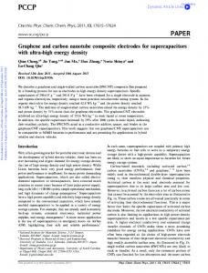
FIG. 1. Atomic force microscope images of annealed Fe on SiO2 / Si as a function of the Fe layer thickness. Note that the scale bar is 1 m for 共a兲, 共b兲, and 共c兲 and 250 nm for 共d兲, 共e兲, and 共f兲. Scans 共e兲 and 共f兲 are high gain and the system noise limits the image quality.
II. EXPERIMENTAL DETAILS
The carbon nanotube films were grown in an ASTEX MWCVD system with microwave frequency of 2.45 GHz and a maximum output power of 1500 W. The same chamber has been used to grow polycrystalline diamond thin films.12 Commercial Si 共100兲 wafers were used as substrates, the wafers were first cleaned in JTB-100 for 15 min to remove surface particles and then rinsed in de-ionized water. Thermally grown SiO2 of 180-nm thickness was used as a buffer layer to prevent the catalyst layer from diffusing and interacting with the silicon and forming a silicide. The catalyst used was iron with different thicknesses 共from 0.3 to 20 nm兲 deposited by e-beam evaporation, and the thickness was monitored by a quartz-crystal oscillator. The substrates were then transferred in situ into another UHV chamber with base pressure ⬍10−9 Torr and annealed at 850 ° C for 10 min. Finally, the substrates were loaded into the MWCVD reactor for CNT growth. The MWCVD chamber was first pumped to 10−3 Torr by a mechanical pump. A rf substrate heating source was turned on, and the temperature was ramped to 650 ° C before the gases were admitted into the chamber. The hydrogen 共H2兲, with a flow rate of 200 SCCM 共standard cubic centimeter per minute兲, was then introduced into the chamber to ignite the plasma. Once the plasma was turned on, the hydrogen was immediately closed and ammonia 共NH3兲 and acetylene 共C2H2兲 in a 4:1 ratio were introduced into the reactor with flow rates of 70 and 18 SCCM, respectively. The substrate temperature was maintained at ⬃850 ° C with heating from both the plasma and the induction heaters. Chamber pressure and plasma power were kept constant at 20 Torr and 600 W, respectively, and the growth time was from 30 to 90 s. The nanotube film growth was carried out under a “bridge” configuration where two Si wafer sections were used as the supports, and another Si wafer section was used to bridge the two supports. The catalyst-covered substrate was positioned partially or fully beneath the bridge, which
served to screen the substrate from the plasma. The nanotube deposition took place underneath the covered regions. We presume that the Si wafer bridge serves to screen the growing CNT from the ions and atomic hydrogen in the plasma. The as-deposited films were characterized by scanning electron microscopy 共SEM兲 共Model JEOL 6400F兲, highresolution transmission electron microscopy 共HRTEM兲 共JEOL 2010F兲, and Raman spectroscopy 共Model ISA J-Y U1000兲. The TEM samples were prepared by sonicating a small amount of the peeled CNTs in methanol for 15 min and drying a few drops of the suspension on a holey carbon or Cu grid. III. RESULTS
Figure 1 shows the atomic force microscopy images of the postannealed Fe samples for varying Fe thicknesses. From Figs. 1共a兲–1共f兲, one can observe that the film thickness affects the island size, shape, and its distribution and consequently, the diameter of the nanotubes 共see Table I兲. For an Fe film thickness of 0.5 nm, the island diameters ranged from 10 to 15 nm, for the 5-nm-thick Fe film the island diameters varied in the range of 60– 120 nm, and for the 20 -nm Fe film, the island diameters ranged from 200 to 600 nm. Our results indicate that the larger film thickness leads to a larger island size, which is in agreement with TABLE I. Variation of the catalyst island size and nanotube diameter with Fe film thickness. Fe film thickness 共nm兲
Island size 共⬃nm兲
Nanotube diameter 共⬃nm兲
20 10 5 2 1 0.3–0.5
200–600 100–200 60–120 30–60 30–50 10–15
100–300 30–120 30–100 15–30 5–15 1–5
Downloaded 18 Jul 2005 to 152.2.4.121. Redistribution subject to AIP license or copyright, see http://jap.aip.org/jap/copyright.jsp
014312-3
J. Appl. Phys. 98, 014312 共2005兲
Wang et al.
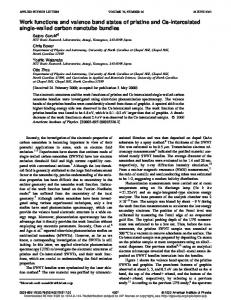
FIG. 2. Scanning electron micrograph of vertically aligned CNT films grown on different thickness Fe catalyst layers. As the Fe film thickness decreases, the diameter of the nanotubes is reduced, the areal density is increased, and the CNTs show improved alignment.
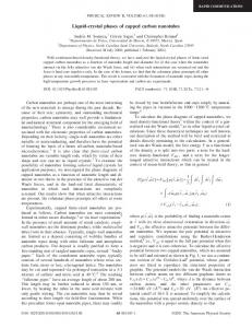
the result by Bower et al.13 The nanotube films grown on these substrates showed a correlation of the nanotube diameter and the island size 共Table I兲. The results indicate that the nanotube diameter is smaller than the size of the Fe catalyst islands. SEM images of vertically aligned CNT films on different thickness Fe catalyst layers exhibit an apparent morphological variation as shown in Fig. 2. The diameters of the nanotubes decrease as the Fe film thickness is reduced from 20 to 1 nm. Figure 2共a兲 indicates that nanotubes grown from the 20-nm Fe layer appear fiberlike with large diameters which ranged from 100 to 300 nm. For the CNT film grown from 10-nm Fe, the structure appears to be similar to the 20-nm film showing complicated surface morphology 共a-C and more protruded tubes兲, and the diameter ranged between 30 and 120 nm. Figures 2共c兲–2共e兲 show carbon nanotube films grown from 5-, 2-, and 1-nm Fe catalyst layers where the CNTs have diameters in the range of 30–60, 10–30, and 5 – 15 nm, respectively. Figure 2共f兲 shows vertically aligned CNT films grown from 0.5-nm Fe, where a dense film with an areal density of ⬃1012 / cm2 was obtained. In order to investigate how the Fe thickness affects the internal structure of the CNTs, the same sequence of CNT films shown in Fig. 2 was characterized by HRTEM 关see Figs. 3共a兲–3共f兲兴. Two important points to be noticed from these figures are 共i兲 the increasing number of walls 共from single and double to multi-兲 and 共ii兲 the variation of the internal structure 共from hollow to bamboolike兲. Figures 3共a兲 and 3共b兲 present HRTEM images of the CNTs grown from 0.3- and 0.5-nm Fe layers, respectively, where the nanotubes are either isolated or loosely bundled and are primarily hollow single- and double-wall CNTs with an average diameter of 5 nm. Figure 3共c兲 shows the CNTs grown from 1-nm Fe, which are double-wall and a few-wall 共multiwall兲 as indicated by white and black arrows, respectively. The former have an average diameter of 5 nm, while the latter are ⬃10 nm, and the number of tube walls is about four. Notice that all tubes exhibit a hollow structure. The film grown from 2-nm Fe has CNT with four or more walls 关Fig. 3共d兲兴. The CNTs grown from the 5-nm Fe layer are shown in the left
and right images in Fig. 3共e兲. The CNT on the left displays 13 walls 共each wall thickness is ⬃0.4 nm兲 with a diameter of ⬃15 nm, and the one on the right has a diameter of ⬃30 nm and approximately 30 walls. The smaller nanotube 关Fig. 3共e兲兴 is hollow and exhibits parallel tubes 共i.e., good crystallinity兲 with a small amount of a-C deposited on the outer walls. The larger nanotube 关Fig. 3共e兲 right兴 displays a periodic bamboolike structure with one or two interlayer共s兲. Figure 3共f兲 shows the CNTs grown from 10- and 20-nm Fe layers on the left and the right of the image, respectively. The nanotube formed on the 10-nm Fe layer has a diameter of ⬃80 nm and exhibits a bamboolike structure with approximately two interlayers separating the tube into many compartments. A nanotube formed on the 20-nm Fe layer resembles a fiber and has more than a few hundred walls and a diameter of ⬃250 nm. The interlayers inside the nanotube almost fill the entire inside space. The variation of growth rate with respect to Fe thickness is shown in Fig. 4共a兲. The growth rate for each sample was determined from the measured film thickness divided by the growth time. The uncertainty represents the variation in the thickness of the sample. The plot is subdivided into three regions 共I, II, and III兲, which relate to the internal structure of the CNT. Below 2 nm, the CNTs are primarily hollow 共I兲, while for an Fe thickness larger than 5 nm, the CNTs observed to have an all bamboolike internal structure 共III兲. Between these limits, the films have CNTs which exhibit either bamboo or hollow internal structures 共II兲. Figure 4共b兲 shows a schematic of the internal structure transition from hollow to bamboolike as noted in Fig. 4共a兲. An interesting observation is that smaller-diameter CNTs 共single and double walled兲 exhibited an almost ten times higher growth rate than the larger-diameter multiwall nanotubes prepared under the same growth conditions. IV. DISCUSSION A. Surface versus bulk diffusion
Prior studies of carbon filament growth by Baker et al. have noted an Arrhenius dependence for carbon filament
Downloaded 18 Jul 2005 to 152.2.4.121. Redistribution subject to AIP license or copyright, see http://jap.aip.org/jap/copyright.jsp
014312-4
Wang et al.
J. Appl. Phys. 98, 014312 共2005兲
FIG. 3. HRTEM of carbon nanotubes grown from 0.3- to 20-nm Fe catalyst layers, 共a兲–共f兲. As the Fe film thickness increases, the number of walls increases from single- and double- to multiwall, and an internal structure transition 共from hollow to bamboolike兲 is observed. Note that the scale bars are 共a兲 5 nm, 共b兲 20 nm, 共c兲 5 nm, 共d兲 5 nm, 共e兲 left 5 nm, 共e兲 right 20 nm, 共f兲 50 nm.
growth on a transition-metal catalyst.14,15 It has been established that the activation energy of the carbon filament growth was similar to the activation energy of carbon bulk diffusion in the transition-metal catalyst.15 This fact also suggests that bulk diffusion may be the rate-limiting step for CNT growth. The growth mechanism for CNTs has been proposed as a combination of the following steps: diffusion of carbon into, saturation of, and precipitation out of the catalyst particles. As far as the internal structure of the tubes is concerned, bamboolike structure has often been observed for MWNTs grown by MWCVD, but the understanding of the origin of the internal layers, which separate the tube body into several compartments, is still rudimentary. It has been suggested that the bamboo structures might be due to the 共i兲 catalyst particle size and shape, 共ii兲 the slow displacement of the catalyst
compared to the growth rate of the CNTs, and 共iii兲 bulk diffusion of carbon in the catalyst.8,10,11 We showed in a previous study that the bulk diffusion of carbon is a significant factor in the formation of the bamboolike structures. In addition to bulk diffusion, there is another path for carbon atoms to transport to the growth edge. Carbon can diffuse along the surface of the catalyst to the growth edge and then be incorporated into the nanotubes. Surface diffusion 共i.e., grain-boundary diffusion兲 is typically a faster process compared to bulk diffusion due to the lower activation energy for surface diffusion.16 B. Proposed growth mechanisms
We discuss the nanotube growth mechanisms in terms of surface and bulk diffusions of carbon. A schematic of this
Downloaded 18 Jul 2005 to 152.2.4.121. Redistribution subject to AIP license or copyright, see http://jap.aip.org/jap/copyright.jsp
014312-5
J. Appl. Phys. 98, 014312 共2005兲
Wang et al.
FIG. 4. 共a兲 Plot of the CNT film growth rate vs Fe thickness where three regions 共I, II, and III兲 with different internal structures are observed. 共b兲 A schematic of the internal structure transition from hollow to bamboolike.
process is shown in Fig. 5. The dashed line represents the base of the nanotube, and the shaded area denotes the projection of the cross-section area of the CNT. Within this description, carbon diffuses 共i兲 across its circumference via surface diffusion for nanotube wall formation and 共ii兲 through the cross-sectional area via bulk diffusion to the top surface of the catalyst for wall and internal-layer formation. For smaller-diameter catalyst particles, surface diffusion is projected as the origin of CNT walls, while for larger catalyst particles surface diffusion may combine with bulk diffusion as the source of wall formation. Bulk diffusion is projected as the primary source for the growth of the internal
structures in characteristic bamboolike CNTs.11 Our model argues that depending upon the competition between surface and bulk diffusions—critically governed by catalyst particle size—different CNT structures can be synthesized. For instance, a hollow structure would be formed for smallerdiameter CNTs nucleated on small particles because surface diffusion predominates. While for larger tubes 共⬎100 nm兲 nucleated on larger particles, where surface and bulk diffusions may be comparable, only characteristic bamboolike structures would be anticipated. Between these extremes, both hollow and bamboolike structures would be expected. Similar to the experiments reported by Baker et al.,15 Hofmann et al.17 and Ducati et al.18 measured the growth rate of nanotubes synthesized by plasma-enhanced CVD 共PECVD兲 using a Ni catalyst. They derived the activation energy from the growth rate to be between ⬃0.23 and 0.76 eV. It was found that the lower bound of these values is quite close to the surface diffusion activation energy value which is ⬃0.3 eV,19 but much less than that of bulk diffusion activation energy of ⬃1.51 eV.20 Their results provide direct support to the proposed mechanism, where surface diffusion is presumed to be the major contribution for the CNT wall growth. For our deposition conditions, the transition occurs for an Fe layer thickness between 2 and 5 nm. For Fe layer thickness beyond the transition point, all of the CNTs have bamboolike structures. Finally, when the catalyst particle size is large enough, carbon fiberlike structures appear, and in our experiments this internal structure is observed at a catalyst layer thickness of 20 nm. It is known that CNT growth by chemical-vapor deposition is a complicated process. Our approach suggests that controlling the catalyst particle size affects the relative bulk and surface diffusion aspects. Alternatively, the surface and bulk diffusions can also be affected by surface chemistry. A study reported by Lee et al.21 observed a decrease in the compartment distance of the bamboolike structures when nitrogen was incorporated in the gas phase. Among other effects, they suggested that nitrogen influenced the surface diffusion rates which affected the internal CNT structure. Other factors such as deposition pressure and temperature,22 the shape of the catalyst, and the sticking coefficient of atoms on the catalyst surface are involved in the growth process, and they should be included in models while predicting the contributions of surface and bulk diffusion. V. CONCLUSION
FIG. 5. A schematic of the growth model based on surface and bulk diffusions. The dashed line represents the growth edge of the nanotube, and the shaded circle denotes a cross section, where carbon diffuses: 共i兲 across its circumference via surface diffusion for nanotube wall formation and 共ii兲 through the cross-sectional area via bulk diffusion to the top surface of the catalyst for internal-layer formation.
In summary, diameter-controlled vertically aligned carbon nanotube films were synthesized by microwave plasma chemical-vapor deposition. Through continuous reduction of the thickness of the iron films, single- and double-wall nanotubes were obtained in contrast with the multiwall nanotubes and nanofibers, which were grown using a larger Fe layer thickness. The results established regimes of catalyst layer thickness where the nanotubes were hollow, bamboolike, and fiberlike. A simple model was proposed which described the growth in terms of surface and bulk diffusion. It established that the transition in structure could be critically governed by
Downloaded 18 Jul 2005 to 152.2.4.121. Redistribution subject to AIP license or copyright, see http://jap.aip.org/jap/copyright.jsp
014312-6
the size of the catalyst particle. Due to the competition between these two processes during growth of nanotubes, diverse internal structures are observed, and we proposed that surface diffusion predominates for thin catalyst layers resulting in hollow and small-diameter nanotubes, while for thicker catalyst layers, bulk diffusion becomes more significant and multiwall, large-diameter nanotubes are formed with bamboolike internal structures. ACKNOWLEDGMENTS
This research work is supported in part by the ONR through the TEC-MURI and the DOE through the ANL CESP program. H. Dai, Surf. Sci. 500, 218 共2002兲. P. J. F. Harris, Carbon Nanotubes and Related Structures 共Cambridge University Press, London, 1999兲. 3 A. M. Fennimore, T. D. Yuzvinsky, W. Han, M. S. Fuhrer, J. Cumings, and A. Zettl, Nature 共London兲 424, 408 共2003兲. 4 W. Huang, S. Fernando, L. F. Allard, and Y. P. Sun, Nano Lett. 3, 565 共2003兲. 5 J. M. Bonard, K. A. Dean, B. F. Coll, and C. Klinke, Phys. Rev. Lett. 89, 197602 共2002兲. 6 K. B. K. Teo, C. Singh, M. Chhowalla, and W. I. Milne, Encyclopedia of Nanoscience and Nanotechnology, edited by H. S. Nalwa 共American Sci1 2
J. Appl. Phys. 98, 014312 共2005兲
Wang et al.
entific Publishers, Stevenson Ranch, CA, 2003兲, Vol. X, pp. 1–22. Y. Y. Wang, G. Y. Tang, F. A. M. Koeck, B. Brown, J. M. Garguilo, and R. J. Nemanich, Diamond Relat. Mater. 13, 1287 共2004兲. 8 L. Yuan, T. Li, and K. Saito, Carbon 41, 1889 共2003兲. 9 C. Ducati, I. Alexandróu, M. Chhowalla, J. Robertson, and G. A. J. Amaratunga, J. Appl. Phys. 95, 6387 共2004兲. 10 V. V. Kovalevski and A. N. Safronov, Carbon 36, 963 共1998兲. 11 C. J. Lee and J. Park, Appl. Phys. Lett. 77, 3397 共2000兲. 12 F. A. M. Kock, J. M. Garguilo, and R. J. Nemanich, Diamond Relat. Mater. 10, 1714 共2001兲. 13 C. Bower, O. Zhou, W. Zhu, D. J. Werder, and S. Jin, Appl. Phys. Lett. 77, 2767 共2000兲. 14 R. T. K. Baker, P. S. Harris, R. B. Thomas, and R. J. Waite, J. Catal. 30, 86 共1973兲. 15 R. T. K. Baker, J. J. Chludzinski, N. S. Dudash, and A. Simoens, Carbon 21, 463 共1983兲. 16 P. Shewmon, Diffusion in Solids, A Publication of The Minerals 共Metals & Materials Society, Pennsylvania, 1999兲. 17 S. Hofmann, C. Ducati, and J. Robertson, Appl. Phys. Lett. 83, 135 共2003兲. 18 C. Ducati, L. Alexandrou, M. Chhowalla, G. A. J. Amaratunga, and J. Roberson, J. Appl. Phys. 92, 3299 共2002兲. 19 J. F. Mojica and L. L. Levenson, Surf. Sci. 59, 447 共1976兲. 20 S. Diamond and C. Wert, Trans. AIME 239, 705 共1967兲. 21 C. J. Lee, S. C. Lyu, H.-W. Kim, J. H. Lee, and K. I. Cho, Chem. Phys. Lett. 359, 115 共2002兲. 22 J.-M. Bonard, M. Croci, C. Klinke, F. Conus, I. Arfaoui, T. Stockli, and A. Chatelain, Phys. Rev. B 67, 085412 共2003兲. 7
Downloaded 18 Jul 2005 to 152.2.4.121. Redistribution subject to AIP license or copyright, see http://jap.aip.org/jap/copyright.jsp