Tzu Yun Chang, Tan Fu Lei, Member, IEEE, Tien Sheng Chao, Senior Member, IEEE, .... C. Lee, âEffect of barrier layer on the electrical and reliability charac-.
IEEE ELECTRON DEVICE LETTERS, VOL. 23, NO. 7, JULY 2002
389
Improvement of Low-Temperature Gate Dielectric Formed in N2O Plasma by an Additional CF4 Pretreatment Process Tzu Yun Chang, Tan Fu Lei, Member, IEEE, Tien Sheng Chao, Senior Member, IEEE, Huang Chun Wen, and Hsiao Wei Chen
Abstract—This study describes a novel technique to form low temperature oxide ( 350 C). Low-temperature oxides were formed by N2 O plasma in the plasma-enhanced chemical vapor deposition (PECVD) system with a CF4 pretreatment. These oxides demonstrate excellent current–voltage ( – ) characteristics comparable to thermally grown oxides. Experimental results indicate that CF4 plasma treatment can significantly improve the reliability of low-temperature oxides. With excellent electrical properties, the technique is highly promising for low-temperature processes. Index Terms—Low-temperature oxide, metal gate, N2 O/CF4 plasma, TDDB and GOI.
I. INTRODUCTION
T
HE SHRINKING size of semiconductor devices has exacerbated the polydepletion phenomenon. Metal replacement gates [1]–[3] are therefore applied to suppress the gate depletion effect and reduce the gate resistance. Replacement gate design involves annealing the source/drain implant before the gate insulator is formed. Conventional oxides grown subsequently by high temperature processes will deviate the existing doping profile. To avoid this deviation, the gate insulator must be formed below 550 C. Plasma-enhanced chemical vapor deposition (PECVD) systems provide an effective means of forming the insulator at low-temperatures (about 350 C). With its slow deposition rate by low RF power (50 W), CVD insulator can produce a high integrity insulator that has been used as high- barrier layer [4]. Therefore, this work presents a novel technique, CF pretreatment, to improve the electric characteristics of either the low temperature oxides, or LTO, as grown by N O plasma. Optimum recipes are also established for this technique. II. EXPERIMENTS MOS capacitors were fabricated on (100)-oriented p-type Si wafers as follows. A field oxide with a thickness of around Manuscript received January 22, 2002; revised April 9, 2002. This work was supported by the National Science Council of Taiwan, R.O.C., under Contract NSC 90-2215-E-009-095. The review of this letter was arranged by Editor C.-P. Chang. T. Y. Chang, T. F. Lei, H. C. Wen, and H. W. Chen are with the Department of Electronic Engineering, National Chiao-Tung University, Hsinchu, Taiwan, R. O. C. T. S. Chao is with the Department of Electrophysics, National Chaio-Tung University Hsinchu, Taiwan, R.O.C., and also with the National Nano Device Laboratories, Hsinchu, Taiwan. Publisher Item Identifier S 0741-3106(02)05978-5.
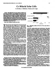
550–600 nm was thermally grown on the silicon wafer by wet oxidation at 1100 C for 50 min. The active area was then defined by photolithography and etched by BOE (buffered oxide etcher) solution. Following the standard RCA cleaning process, CF plasma treatment (30 s in the same PECVD system) was performed before PECVD oxide formation. Next, low temperature oxides were formed in N O plasma with RF power of 50 W at 300 C for 90 and 180 s, thickness was 2.9 and 3.1 nm, respectively. For comparison, a thermal oxide with thickness of 3.2 nm was grown at 900 C. Oxide thickness was measured by ellipsometer. TiN metal was deposited by sputtering to serve as the gate electrode. All processing temperatures were lower than 400 C after formation of the gate dielectric. Finally, all samples were deposited with a 500-nm Al film by thermal evaporation. The metal pad area was defined by photolithography and a wet chemical etching solution. After a substrate contact was formed by backside Al deposition, a sintering was performed in a N ambient at 400 C for 20 min. Characteristics of ultrathin gate oxides, i.e., effective oxide thickness, breakdown field, leakage current, and time dependent dielectric breakdown, were measured by using HP4156, HP4284 and Keithley CV. Three different high fields were used to measure the time-to-breakdown for ten years lifetime extrapolation. III. RESULTS AND DISCUSSION Exactly how the proposed CF pretreatment method affects PECVD LTO is described first. A low temperature process was maintained by depositing a TiN metal gate to replace the conventional poly-Si gate. Fig. 1(a) presents the – characteristics of PECVD oxide with/without CF treatment and thermal oxides. The oxide was formed by N O plasma for 90 s. According to our results, as-deposited samples, or “90 s,” show the largest leakage current among these the samples due to plasma damage. However, CF pretreatment sample exhibits a significant reduction of leakage that is comparable to that of thermal oxide. This improvement appears to be owing to the formation of strong Si–F bonds. Fig. 1(b) shows – curves using a longer processing time (180 s). Although a longer plasma time generally causes significant damage on the film, according to our results, CF pretreatment sample shows an excellent performance, even approaching that of thermal oxides. With CF treatment, a longer N O plasma time is preferred to a shorter one. According to our experimental data (not shown), the deposition
0741-3106/02$17.00 © 2002 IEEE
390
IEEE ELECTRON DEVICE LETTERS, VOL. 23, NO. 7, JULY 2002
(a)
(a)
(b) (b) Fig. 1. The J –V characteristics of low-temperature oxides with/without CF treatment and thermal oxides; the N O plasma deposition time is (a) 90 s and (b) 180 s. The capacitor area is 9 10 cm . The electrical thickness of 90 s CF , 90 s, thermal (90 s), 180 s CF , 180 s, and thermal (180 s) is 37 2, 35 2, 34 0.5, 39 2, 37 2, and 37 0.8 Å.
+
6
6
6
2 + 6
6
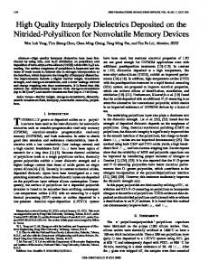
Fig. 2. (a) Oxygen and (b) fluorine ESCA spectrum of oxides with/without CF treatment. Normalized C –V curves are shown in the insert of Fig. 2(a). No striking difference is observed.
6
rate by N O plasma oxides saturated at 90 s. Notably, excessive N O plasma densifies the low-temperature oxide and only slightly increases the thickness. Therefore, the low-temperature oxide formed by N O plasma (for 180-s) with CF pretreatment could effectively improve the current–voltage ( – ) characteristics similar to thermal oxides. To identify the effect of CF treatment on LTO, electronic spectrum-scope for chemical analysis (ESCA) was applied on samples with/without CF treatment. Fig. 2 (a) and (b) shows the intensity of oxygen and fluorine incorporation, indicating that CF treatment increases not only the incorporation of fluorine into oxides but also the amount of Si–O bonds. According to a previous study, fluorine can catalyze the movement of excess oxygen in the dielectric bulk, subsequently reacting at the interface and increasing the oxide thickness [5]. Such a
reaction involves: the availability of un-reacted oxygen, the transportation of the oxygen to the interface, and the formation of silicon dioxide [6]. Normalized capacitance–voltage ( – ) curves with or without CF treatment are shown in the insert of Fig. 2(a). No striking difference is observed. – measurement is used to reconfirm the electrical thickness. The respective oxide thickness of CF pretreated LTO, LTO, and thermal oxide is 37 2, 35 2, and 34 0.5 Å. Experimental results indicate not only that oxides formed in PECVD system at low temperature exhibit a poor uniformity, but also that additional CF treatment increases the electrical oxide thickness of about 2 Å. Above results, clearly indicate that CF treatment can improve the quality of LTO by replacing dangling bonds with stronger Si–F or Si–O bonds. Here, time dependent dielectric breakdown (TDDB) was measured, with those results shown in Fig. 3. The CF pretreated data were scaled from 3 10 cm to 0.1 cm and, finally, the 0.01%-line was calculated [7],
CHANG et al.: IMPROVEMENT OF LOW-TEMPERATURE GATE DIELECTRIC
391
IV. CONCLUSION Results in this study demonstrate that an additional CF treatment before N O plasma can improve – characteristics of PECVD LTO and achieve a performance as thermal oxides. Additionally, gate oxide integrity (GOI) can be improved by replacing dangling bonds with stronger Si–F bonds. Moreover, the reliability of LTO is also improved by CF treatment. The high performance of LTO makes it a promising alternative for the gate insulator in the replacement gate CMOS application. This process can also facilitate the formation of LTO for thin-film transistors or use in TFT industrial applications. REFERENCES
Fig. 3. TDDB plot of thermal oxides and low-temperature oxides with/without CF treatment.
[8]. According to our results, the operation field of the N O sample is 5.5 MV/cm for 10 years lifetime. Additionally, CF treatment sample increases the operation field to 6.2 MV/cm. This observation confirms that the proposed CF treatment method can improve the oxide integrity. However, the reliability of thermal oxides is better than that of low temperature oxides with CF treatment. The low temperature process ( 350 C) can not anneal defects or traps during plasma fabrication and degrades the oxide reliability. Nevertheless, low temperature oxides with CF treatment are highly promising for thin-film transistor applications.
[1] A. Chatterjee et al., “CMOS metal replacement gate transistors using tantalum pentoxide gate insulator,” in IEDM Tech. Dig., 1998, pp. 777–780. [2] J. M. Hergenrother et al., “The vertical replacement-gate (VRG) MOSFET: A 50-nm vertical MOSFET with lithography-independent gate length,” in IEDM Tech. Dig., 1999, pp. 75–78. [3] C. P. Chang et al., “SALVO process for sub-50 nm low-Vt replacement gate CMOS with KrF lithography,” in IEDM Tech. Dig., 2000, pp. 53–56. [4] Y. Jeon, B. H. Lee, K. Zawadzki, W.-J. Qi, A. Lucas, R. Nieh, and J. C. Lee, “Effect of barrier layer on the electrical and reliability characteristics of high-k gate dielectric films,” in IEDM Tech. Dig., 1998, pp. 797–800. [5] P. Wright and K. Sarawat, “The effect of fluorine in silicon dioxide gate dielectrics,” IEEE Trans. Electron Devices, vol. 36, pp. 879–889, May 1989. [6] T. B. Hook, E. Adler, F. Guarin, J. Lukaitis, N. Rovedo, and K. Schruefer, “The effects of fluorine on parametrics and reliability in a 0.18-�m 3.5/6.8 nm dual gate oxide CMOS technology,” IEEE Trans. Electron Devices, vol. 48, pp. 1346–1353, July 2001. [7] R. Degraeve, N. Pangon, B. Kaczer, T. Nigam, G. Groeseneken, and A. Naem, “Temperature acceleration of oxide breakdown and its impact on ultra-thin gate oxide reliability,” in Symp. VLSI Technology, 1998, pp. 59–60. [8] R. Degraeve, G. Groeseneken, R. Bellens, J. L. Ogier, M. Depas, P. J. Roussel, and H. E. Maes, “New insights in the relation between electron trap generation and the statistical properties of oxide breakdown,” IEEE Trans. Electron Devices, vol. 45, pp. 904–911, Apr. 1998.