oxide must remain relatively free from stress-induced electron and/or hole ... 344. IEEE ELECTRON DEVICE LETTERS, VOL. 18, NO. 7, JULY 1997 preserved ...
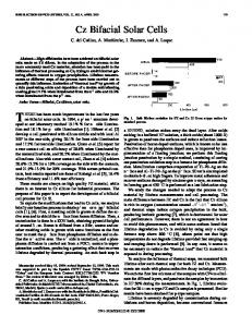
For individual use by an IEEE Electron Devices Society member purchasing this product. IEEE ELECTRON DEVICE LETTERS, VOL. 18, NO. 7, JULY 1997
343
Improved Flash Cell Performance by N O Annealing of Interpoly Oxide Fuh-Cheng Jong, Tiao-Yuan Huang, Fellow, IEEE, Tien-Sheng Chao, Horng-Chih Lin, Len-Yi Leu, Konrad Young, Member, IEEE, Chen-Hsi Lin, and Kuang Y. Chiu, Senior Member, IEEE
Abstract—In this letter, we report the effects of N2 O annealing of interpoly oxide on flash cell performance. It is demonstrated that by adding an N2 O anneal after interpoly oxide formation, improved cycling endurance is achieved. The program and erase efficiencies are also improved significantly, compared to the control cell without N2 O anneal. The cells with N2 O anneal show higher cell current (i.e., drain current), which can be ascribed to a lower threshold voltage and higher transconductance, compared to the control cell.
I. INTRODUCTION
E
EPROM write/erase cycling endurance of greater than 100 K is desirable for industrial applications. This places a stringent requirement on the EEPROM’s oxide quality, as the oxide must remain relatively free from stress-induced electron and/or hole trapping after being subjected to the program and erase cycling stress for over 100 K times. Recently, a flash cell with a horn-shaped floating-gate, as shown in the inset of Fig. 1, has been proposed by Silicon Storage Technology, Inc. (hereafter called SST cell) for enhancing the erase efficiency [1]. The SST cell utilizes the bird’s beak created by a LOCOStype oxidation performed on the polysilicon to form the tip of the horn on the floating-gate. The high programming efficiency of the cell is achieved by source-side hot electron injection [2], [3]; while enhanced interpoly Fowler–Nordheim tunneling from the tip of the horn of the floating gate to the select gate (i.e., control gate) is used for sector erase. For the SST cell, it is very difficult to achieve write/erase cycling endurance of over 60 K. This is because the erase path is from the sharp tip of the horn of the floating gate to the control gate (as shown in the inset of Fig. 1). During erase, the electrons escape the floating-gate by tunneling through the interpoly oxide. Since the interpoly oxide quality, especially that grown on the sharp tip of the horn, is in general worse than that grown directly on top of the single-crystal silicon, Manuscript received November 6, 1996; revised March 10, 1997. This work was supported by the R.O.C.’s National Science Council under Contracts NSC85-2215-E009-039, NSC86-2215-E009-046, and NSC86-2722-2317-001. F. C. Jong is with the Department of Electronic Engineering, National Chiao-Tung University, Hsinchu 300, Taiwan, R.O.C., and Winbond Electronics Corporation, Hsinchu 300, Taiwan, R.O.C. T.-Y. Huang is with the Department of Electronic Engineering, National Chiao-Tung University, Hsinchu 300, Taiwan, R.O.C., and the National Nano Device Laboratories, Hsinchu 300, Taiwan, R.O.C. T.-S. Chao and H.-C. Lin are with the National Nano Device Laboratories, Hsinchu 300, Taiwan, R.O.C. L.-Y. Leu, K. Young, C.-H. Lin, and K. Y. Chiu are with the Winbond Electronics Corporation, Hsinchu 300, Taiwan, R.O.C. Publisher Item Identifier S 0741-3106(97)05086-6.
Fig. 1. The write/erase cycling endurance of the split-gate flash cell for the samples with ( ) and without ( ) N2 O anneal. Cell current in the “1” state remains higher than 40 �A (i.e., minimum current required for the sense amplifier to sense as “1”) for the cell with N2 O anneal, even after 100 K erase/write cycling endurance.
poor cycling endurance is normally observed. Recently, N O annealing has been applied to the thin tunneling oxide (i.e., first gate oxide grown on top of the single-crystal silicon) in the EEPROM for improving the cell performance, such as better endurance, and programming efficiency [4]–[6]. The characteristics of polysilicon oxide grown in pure N O have also been reported [7]. In this letter, we show, for the first time, that by adding an N O-annealing step after interpoly oxide formation, significant improvement in SST cell’s write/erase cycling endurance, as well as program and erase efficiencies can be achieved. II. EXPERIMENTS A standard 0.8- m, double-level polysilicon CMOS process using 6-in wafers was used to fabricate the SST cells used in this study. After forming a 15-nm first gate oxide, a 170-nm polysilicon layer was deposited, followed by the deposition of a 150-nm silicon nitride layer. The silicon nitride layer was then selectively removed with a reversegate mask, so as to expose the floating-gate region. Wafers were then oxidized to form a LOCOS-type polyoxide on top of the exposed polysilicon layer [1]. The remaining nitride layer was then stripped by hot phosphoric acid, exposing the underlying polysilicon layer. The exposed polysilicon layer was subsequently etched away, while the remaining polysilicon layer underlying the LOCOS-type polyoxide was
0741–3106/97$10.00 1997 IEEE
For individual use by an IEEE Electron Devices Society member purchasing this product. 344
IEEE ELECTRON DEVICE LETTERS, VOL. 18, NO. 7, JULY 1997
preserved during the polysilicon etch, as the LOCOS-type polyoxide serves as a hard mask during the etch, thus leaving the horn-shaped floating gate underneath the LOCOS-type polyoxide. Wafers were then split to receive the polyoxide oxidation. For the control split, the polyoxide was grown by a conventional O oxidation. While for the N O-annealed split, polyoxide was first grown in O oxidation, followed by an N O anneal for 15 min at 925 C Both splits have comparable final polyoxide thickness. Afterwards, a second polysilicon layer was deposited, saturation-doped, and patterned to form the control gate of the cell. For the write/erase cycling endurance test, a 14-V, 800s pulse was applied to the control gate, while the source and drain were grounded, so as to facilitate interpoly Fowler–Nordheim tunneling for the erase operation. For programming the cell with source-side hot-electron injection, the drain was held at 12 V, the source at 0.6 V, the substrate at ground, and a 2-V, 800- s pulse was applied at the control gate. After each write/erase cycling, the cell current was read by applying 4 V to the control gate, 2 V to the source, while the substrate and drain were held at ground. For the program efficiency test, the control gate was held at 2 V, the source at 0.6 V, the substrate at ground, and the drain voltage was varied in magnitude and duration, and the cell current was read after each programming. Finally, for the erase efficiency test, all terminals were grounded, while the control gate was varied in magnitude and duration, and the cell current was read after each erase.
III. RESULTS
AND
(a)
(b) Fig. 2. The program efficiency for cells (a) without and (b) with N2 O anneal. Significant improvement is achieved for the N2 O-annealed cell. Note the scale difference on the vertical axis for two plots.
DISCUSSION
The results on the write/erase cycling endurance of the SST split-gate flash cells are shown in Fig. 1. It can be seen that the cell read current in the “1” (i.e., “erase” or low threshold) state is much higher for the cell with N O anneal. Specifically, the initial cell current is about 140 A for the N O-annealed cell, while the initial cell current is only about 110 A for the control cell. Furthermore, the cell current in the “1” state remains higher than 40 A (i.e., minimum current required for the sense amplifier to sense as “1”) for the cell with N O anneal, even after 100 K erase/write cycling endurance. While for the control cells, it is very difficult to achieve a cycling endurance of over 50 K. We believe the higher initial cell current of the N O-annealed cell can be ascribed to a better capacitve coupling between the control gate and the floating-gate, due to the formation of an interfacial silicon oxynitride layer [8], as the nitrogen is known to pile up around the polysilicon floating-gate [9]; or a smaller acceptor-type interface state on the polyoxide near the floating gate, which will in turn result in a smaller threshold voltage of the cell. The smaller threshold voltage accounts for the higher cell current of the N O-annealed cells. The “window closure” (i.e., decrease in cell read current in the erased state) after write/erase cycling in our cell is believed to be due to the build-up of electron trapping and electron trap generation between the control gate and the tip of the floating-gate as a result of the write/erase cycling [9], causing a “shielding effect” thus reducing the efficiency of the electrons being pulled out from the floating
(a)
(b) Fig. 3. The erase efficiency for cells (a) without and (b) with N2 O anneal. Significant improvement is achieved for the N2 O-annealed cell.
gate during “erase” operation. A slower window closure rate observed on the N O-annealed cells could be explained by a reduced electron traps by the N O-anneal [9]. The program and erase efficiencies are also studied. As shown in Fig. 2, significant improvement in programming
For individual use by an IEEE Electron Devices Society member purchasing this product. JONG et al.: IMPROVED FLASH CELL PERFORMANCE
efficiency is achieved by the N O anneal. For example, it takes 7.5 V at the drain for about 10 s for the N O-annealed cell, while it will take 7.5 V for more than 3500 s for the control cells to achieve the same programming results. Substrate current measurements also confirm that SST cells annealed by N O depict larger substrate current than the control cell without N O anneal (data not shown). The erase efficiencies are plotted in Fig. 3. Again better erase efficiency is achieved for the N O-annealed cells. The better erase efficiency can again be explained by a better capacitive coupling or a reduced interface state density on the N O-anneal cells, which results in an enhanced Fowler–Nordheim tunneling between the control gate and the floating gate. Detailed mechanisms are still under investigation, and will be reported later.
IV. CONCLUSION In this letter, we demonstrate that the cycling endurance of flash cell with N O-annealed interpoly oxide can be improved to over 100 K, which is normally difficult to achieve for the SST cell with horn-shaped floating gate used in this study. The program and erase efficiencies are also significantly improved over the control cell without N O anneal. These improvements could be explained by a better capacitive coupling between control gate and floating gate or a smaller acceptor-type interface state density on the N O-annealed polyoxide, causing a threshold voltage reduction and better initial cell current for the N O-annealed samples.
345
ACKNOWLEDGMENT The authors would like to thank Windbond’s processing fab for processing the wafers, and National Nano Device Laboratories for N O annealing. REFERENCES [1] S. Kianian, A. Levi, D. Lee, and Y. W. Hu, “A novel 3-V-only, small sector erase, high-density flash E2 PROM,” in Proc. Symp. VLSI Technol., 1990, pp. 71–72. [2] A. T. Wu, T. Y. Chan, P. K. Ko, and C. Hu, “A novel high-speed, 5-V programming EPROM structure with source-side injection,” in IEDM Tech. Dig., 1986, pp. 584–587. [3] F. V. Houdt, G. Groeseneken, and H. E. Maes, “An analytical model for the optimization of source-side injection Flash EEPROM devices,” IEEE Trans. Electron Devices, vol. 42, pp. 1314–1320, July 1995. [4] H. Fukuda, M. Yasuda, T. Iwabuchi, and S. Ohno, “Novel N2 Ooxynitridation technology for forming highly reliable EEPROM tunnel oxide films,” IEEE Electron Device Lett., vol. 12, pp. 587–589, Nov. 1991. [5] U. Sharma, R. Moazzami, P. Tobin, Y. Okada, S. K. Cheng, and J. Yeargain, “Vertically-scaled, high-reliability EEPROM devices with ultrathin oxynitride films prepared by RTP in N2 O/O2 ambient,” in IEDM Tech. Dig., 1992, pp. 461–464. [6] H. Fukuda, A. Uchiyama, T. Kuramochi, T. Hayashi, T. Iwabuchi, T. Ono, and T. Takayashiki, “High-performance-scaled flash-type EEPROM’s with heavily oxynitrided tunnel oxide films,” in IEDM Tech. Dig., 1992, pp. 465–468. [7] C. S. Lai, T. F. Lei, and C. L. Lee, “The characteristics of polysilicon oxide grown in pure N2 O,” IEEE Trans. Electron Devices, vol. 43, pp. 326–331, Feb. 1996. [8] T. S. Chao, W. H. Chen, S. C. Chen, and H. Y. Chang, “Characteristics of oxide grown by N2 O,” J. Electrochem. Soc., vol. 140, no. 10, pp. 2905–2908, 1993. [9] H. Hwang, W. Ting, D. L. Kwong, and J. Lee, “Electrical and reliability characteristics of ultrathin oxynitride gate dielecrtric prepared by rapid thermal processing of N2 O,” in IEDM Tech. Dig., 1990, pp. 421–424.