IMPROVING EXTERNAL MEMORY ACCESS FOR ... - CiteSeerX
Recommend Documents
Lars Arge1â, Darren Erik Vengroff2ââ, and Jeffrey Scott Vitter3âââ. 1 BRICSâ , Department of ...... L. Arge, M. Knudsen, and K. Larsen. A general lower bound ...
including trapezoid decomposition, batched planar point location, tri- angulation ..... nd the segment directly below each endpoint|see Figure 2 for an example ... diately above A. Similarly, we solve EPD with negated y coordinates and a.
10. System Throughput (M bytes/sec). Number of Concurrent Sorts. Sort Job Set : D2 memory-static sort memory-adaptive sort. Figure 6: Throughput of D2. 1. 1.5.
CCR-9904943, the Department of Energy's Accelerated Strategic Computing Initiative under research ... ratory Computer Science Institute (LACSI) through LANL contract number ...... Unlike moldyn and magi, which have respective degrees of.
to O(Nlog2 7); the recursive nature of such algorithms place a large burden on ... Matrix multiplication is a common problem in comptuer science, that is expensive to solve with a complexity of O(N3). ... used, as well as how it leads us to be able t
pose three questions that we believe will shape the future development and use of this ... nursing facility), where for a while they typically have access to outpatient care or ..... Virtual Reality 2001, J. D. e. a. Westwood, Ed.: IOS Press, 2001, p
data structures are often designed and analyzed using the parallel disk ... Key words and phrases. external memory, secondary storage, disk, block, ...... In particular, the matrix can be broken up into ..... concurrency and recovery to B-trees.
stores a multi-set of items from an ordered universe. We equate items with their .... pute an Euler tour on the resulting directed graph. Break the tour at the root.
online data structures for external memory, some very old and some very new, such as ... and data structures that bypass the virtual memory system and explicitly manage their own I O. We refer to such ...... concurrency, recovery and node consolidati
... be able to retrieve it when you need it. If you don't, then you'll forget it. ... use visual aids to help you remember, if audio is your thing, record yourself reading ...
this in a deterministic list ranking algorithm. Department of Computer Science, Box 1910, Brown Univer- sity, Providence, RI 02912{1910. ySupported in part by ...
variety of external memory types, such as SRAM, SDRAM, and DDR, and addresses larger storage capacities compared to OCM, it has one major drawback.
Liviu Iftode, Cezary Dubnicki, Edward W. Felten and Kai Li. Department of Computer Science. Princeton University. Princeton, NJ 08544. Abstract. Shared virtual ...
Morton [27] or Hilbert [17] space-filling curves create a linear ordering of ...... [25] S. Mukherjee, S. Sharma, M. Hill, J. Larus, A. Rogers, and. J. Saltz. Efficient ...
Phillip L. Morgan, John Patrick, Samuel M. Waldron, Sophia L. King, and Tanya Patrick .... Jones, 2006a), although the effectiveness of using a mouse cursor.
EXTERNAL MEMORY TECHNIQUES FOR ISOSURFACE EXTRACTION 3 Figure 1. Typical isosurfaces are shown. The upper two are for the Blunt Fin dataset. The ones in the bottom ...
Apr 24, 2008 ... and data structures. This book is originally published as. Foundations and Trends
. ® in Theoretical Computer Science. Volume 2 Issue 4, ISSN: ...
email: {nikolov, stefanov, edd}@liacs.nl. ABSTRACT ..... by blocking write/read on these fifos. The External Data Memory Controller (EDM CTRL) is responsible.
AbstractâBulk memory copying and initialization is one of the most ubiquitous .... 150%. 160%. Apache-recv. Apache-send. Iperf-recv. Iperf-send. Iozone3. Avg.
Flash memory is a storage medium that is becoming more and more popular. Though ... We derive and define three performance parameters, namely, utilization ...
alternative scheme, and 1.5Ãâ2Ã of a highly optimistic DMA with zero setup and interrupt overheads. Keywords-memory copying; memory initialization; cache.
However, when a specific application is targeted for hardware acceleration ... velopment of a custom application-specific memory system which exploits reuse.
Mar 2, 2001 - tailed exposition is given by Sutton and Barto [23].) With the parameter λ set ..... Morgan Kaufmann. [23] Richard S. Sutton and Andrew G. Barto.
describes the Remote Memory Access Protocol for SpaceWire which provides a ... A SpaceWire router chip has been designed by University of Dundee and is.
IMPROVING EXTERNAL MEMORY ACCESS FOR ... - CiteSeerX
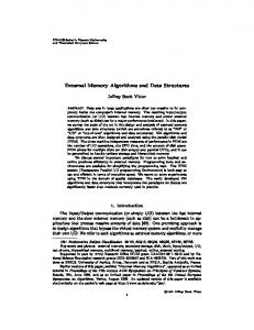
SDRAM. Controller. SDRAM Chip. S. Arbitrator. Data. Memory. S. S. Tri-State Bridge. S .... nents tasks to process large data blocks in the DDR memory.
IMPROVING EXTERNAL MEMORY ACCESS FOR AVALON SYSTEMS ON PROGRAMMABLE CHIPS. Hendrik Eeckhaut, Mark Christiaens, Phillipe Faes, Dirk Stroobandt Parallel Information Systems ELIS, Ghent University Sint-Pietersnieuwstraat 41, 9000 Ghent, Belgium email: [email protected] ABSTRACT
automate system integration tasks. Gaisler Research developed GRLIB for system-on-chip development [2]. In contrast to XPS and SOPC, GRLIB provides a vendor-independent infrastructure for reusable IP cores. In this paper we explore the options of accessing external dynamic memories in FPGA designs with the SOPCbuilder tool. We investigated the different options to optimize system bandwidth for custom components. We present a new hardware design pattern to reuse existing IP cores and improve memory transfer efficiency. In Sections 2 and 3 we present SOPC-builder and the standard approach to develop custom hardware components. In Section 4 we present our new methodology and we quantify the improvements by building and measuring a real design. We conclude this paper with a possible third option (Section 6) and the conclusions.
In this paper we present a new hardware design pattern for improving memory transfers to external dynamic memory in Altera’s SOPC-builder tool by reusing the standard DMA IP core for all bulk memory transfers without the need for a CPU. The presented approach doubles the data throughput without the need for extra system resources. In addition it is more effective for choosing optimal clock settings for the different components of the system on a programmable chip. The benefits and limitations of this new approach are illustrated with a real world example: a bitplane assembler for scalable wavelet based video. The new design is 2.3 times faster with the same clock settings as the original design and uses about 100 logic elements less. Applying our new approach also has a positive impact on energy consumption. 1. INTRODUCTION
2. SOPC/AVALON
To be competitive in todays market, electronics products became very complex, leading to the implementation of entire Systems-on-a-Chip (SoC). Yet, overwhelming pressure exists for designers to reduce development time and costs. A high level of design reuse among design groups is needed to attain the high productivity rates in SoC design. To efficiently reuse IP, a solid integration platform is vital. An integration platform is a SoC design environment that includes architectural specifications and pre-qualified IP blocks designed to work together on that platform. For reconfigurable platforms (FPGAs) multiple tools and libraries exist that support designers in system design and integration. Xilinx offers the Xilinx Platform Studio (XPS) for creating custom embedded platforms [1]. XPS is an integrated development environment which contains a wide variety of embedded tools, IP, libraries and design generators to assist the system designers. Altera offers SOPC-builder to
SOPC Builder [3] is a software tool that enables to rapidly and easily build and evaluate embedded systems on Altera devices. Essentially it is a system-generation tool that lets you define, parameterize, link, and integrate IP cores (such as soft processor, DSP, communication and memory controller cores) in the company’s high-density-programmablelogic devices. The tool automatically generates interconnect logic (Avalon system interconnect fabric [4]) in response to the components (or cores) specified by the designer. This reduces the amount of time designers must spend on peripheral integration and increases their ability to reuse peripherals in subsequent designs. The system interconnect fabric uses minimal FPGA logic resources to support address decoding, wait-state generation, peripheral address alignment, interrupt-priority assignment, data path multiplexing and clock domain crossing. Figure 1 illustrates the interconnect fabric of an example design. In contrast to a traditional bus in a processor-based system, which lets only one bus master access the bus at a time, the Avalon system interconnect fabric uses a slave-side ar-
This research is supported by the I.W.T., grant 020174, the F.W.O., grant G.0021.03, the GOA project 12.51B.02 of Ghent University and the Altera university program.
Fig. 2. Detailed view of multi-master Avalon connections [5]. Two master ports are connected to a shared slave port. The arbitrator logic has to multiplex all addresses, data and control signals.
Tri-State Bridge
S
S
S
Instruction Memory
Data Memory
SDRAM Controller
S
S
Ethernet MAC/PHY Chip
Flash Memory Chip
SDRAM Chip Component Hardware
Write Data & Control Signals
M
Avalon-MM Master Port
S
Avalon-MM Slave Port
Read Data Interface to Off-Chip Device
Register File Status Register
ApplicationSpecific Interface Signals
Fig. 1. System interconnect fabric block diagram of an example system designed with SOPC builder [5].
Control Register1 Control Register2
Task Logic
Data Register1
Avalon-MM Slave Interface
Avalon-MM Slave Port Signals
Data Register2 Data Register3
Other Registers
bitration scheme. Slave-side multi-master arbitration eliminates the bottleneck for access to a shared bus, because the system does not have shared bus lines. Avalon masterslave pairs are connected by dedicated paths. A master port never waits to access a slave port, unless a different master port attempts to access the same slave port at the same time. As a result, multiple master ports can be active at the same time, simultaneously transferring data with independent slave ports. Figure 2 illustrates some more details of multi-master systems. SOPC Builder generates an arbitrator for every slave that is connected to more than one master port. All details about arbitration are encapsulated inside the system interconnect fabric. As a result a component in a single-master design can be reused in multi-master systems without modifications. Arbitration settings are configurable per slave port. For a complete specification of the Avalon interconnection fabric and SOPC-Builder, we refer to [4] and [5].
Fig. 3. Typical SOPC component with one Avalon slave port [5].
when a master (e.g. a NIOS CPU in Figure 1) is available to initiate the transfers. If the custom component wants to directly access external memories it needs an Avalon master port. Implementing a master port is very straightforward. The component needs only a small finite state machine (FSM) to handle the Avalon interface protocol. SOPC automatically generates the interconnection fabric that takes care of arbitration and clock domain crossings. It also handles the details of transferring data with memories with differing data widths.
3. CUSTOM SOPC COMPONENT DESIGN
The major disadvantage of this approach is its resulting memory bandwidth performance when accessing dynamic memories. Memory operations to sequential addresses are handled separately and thus miss the improved performance of using burst transfers. Moreover adding a lot of masters to the same slave (i.e. the external memory) makes the arbitration logic very large and thus limits its maximum clock frequency (see later).
A typical custom SOPC-component has just one interface with the rest of the system: one Avalon slave port to control the component (Figure 3). This memory mapped (MM) interface only responds to transfer requests. It can not initiate transfers itself. The standard method to input and output data is through memory mapped registers as illustrated in Figure 3. This is OK for small or streaming data transfers
312
M S Component 0
M Component 0 S
S
S
M DDR
S
M Component 1 S
M
DMA
S
S
PCI
M
DDR
S
S Component 1
Test & Set
S
M
DMA
S
S
PCI
M
Control (via PCI)
Control (via PCI)
External controller
External controller
Fig. 4. The figure on the left illustrates the standard approach with multiple masters. This design can be transformed to the design on the right, which uses the DMA core for all memory transfers. The orthogonal arrows illustrate the Avalon communication signals from master to slave, the curved arrows illustrate the resulting memory transfers. M is a master port, S a slave port. Actually the DMA core has two separate master ports, a read and a write port, but they are displayed as one port for clarity. 4. USING A DMA IP-CORE
that is controlled over a PCI-bus. In the original design (Figure 4 left) the system has two custom components that are master of a DDR memory. The system also has a DMA core that is used by an external CPU to fastly read and write to the DDR memory. The custom components are controlled by the external CPU, over the PCI-bus, which gives the components tasks to process large data blocks in the DDR memory.
We found that the bandwidth could be seriously improved by making creative reuse of Altera’s direct memory access (DMA) core [6]. This core was originally developed as an embedded CPU (NIOS) peripheral to offload memory transfer tasks as illustrated in the example of Figure 1. The DMA core can perform bulk data transfers, reading data from a source address range and writing the data to a different address range, while the CPU is free to perform other tasks in parallel. The DMA controller transfers the data as efficiently as possible, reading and writing data at the maximum pace allowed by the source or destination. We engineered a methodology to reuse this core to boost the memory bandwidth of custom components at the cost of some added design complexity without the need for a CPU. The master port, connected to the external memory in the standard approach, is replaced with a master port to the DMA control slave port, and a slave port which exposes the components local memory buffer. Furthermore a test-andset synchronisation SOPC-component is necessary to guarantee mutual exclusive access to the DMA core when using multiple components that request external memory accesses. This very simple extra component uses interrupts to notify the components when the DMA core is available for new requests. The methodology is illustrated in Figure 4 for a system
To improve the memory bandwidth to the components and alleviate the multi-master bottleneck the design can be transformed to the design on the right of Figure 4. The DDR now only has one master, the DMA. The master ports of the components are replaced with slave ports through which the DMA core can write to the component’s memory buffers. Each of the components is extended with a master port to request exclusive access to the DMA core and once the access is granted, to request DMA transactions. The necessary changes to the internals of the component are illustrated in Figure 5. To avoid wasting time with polling, the DMA core uses interrupt requests to notify its masters that transfers are completed. Similarly the test-and-set component uses interrupt requests to notify its masters that another component can request exclusive access to the DMA core. For clarity the interrupts are not displayed in Figure 4 and 5. The most important advantage of this new approach is that the DMA can now transfer data at the highest efficiency
313
Mem Calc core
M Mem FSM
Contr FSM
DMA FSM
Mem S
S
Fig. 6. Quality scalability: the wavelet transformed frames are displayed as height fields (height=absolute value of wavelet coefficient). Decoding more bitplanes results in a more accurate wavelet-transformed frame. The distortions of the images on the bottom row are slightly exaggerated for visual clarity.
M
Calc core Contr FSM
S
Wavelet Entropy Decoder
Fig. 5. The necessary changes to the component when using the new approach. Only the memory communication FSM and the component’s interface have to be rewritten
Bitplane Assembler
Fig. 7. Illustration of the bitplane assembler. between the different memories in the system. The component only needs a relatively simple FSM to request the DMA transfers; The DMA core does all the hard work. The second large advantage is that this methodology allows to more efficiently divide clock domains. In the original approach the master, who initiates the memory transfer, operates at the clock frequency of the component. If this frequency is different from the memory frequency, synchronization logic is required, which slows down memory transfers. In the new approach, the clock domain crossing can be synchronized by the component’s data buffer. The hardware of this buffer, a dual port memory, can do this without extra logic. This way the memory transfers can be completed without speed reduction, independent of the component’s clock. Another pleasant advantage of this approach is that observability of the component increases because the data buffer of the component is now externally visible (and editable). This is very useful for debugging. The fact that the DMA, instead of the DDR, now has multiple masters is not critical since the DMA slave port is only used for control instructions and not for data transfer. Hence the data width of the DMA slave port is usually smaller and the communication over this connection can be handled at lower clock frequencies. The arbiter of the DMA slave port in the new approach will be significantly smaller (and faster) than the arbiter for the DDR-slave in the original method. Because all memory transfers are now performed by the
314
DMA core, only the transfers that are supported by the DMA core are possible. This implies a few restrictions, such as alignment and minimum transfer size (i.e. coarser granularity), to feasible memory transfers. 5. CASE STUDY: A BITPLANE ASSEMBLER FOR SCALABLE VIDEO To quantify the consequences of using the new methodology we implemented a custom component, a bitplane assembler (AS), with both approaches. This AS component is a part of an FPGA implementation of a wavelet-based scalable video codec [7]. To support quality scalability this codec encodes wavelet frames bitplane by bitplane (from most significant to least significant), yielding progressive accuracy of the wavelet coefficients as illustrated in Figure 6. The task of the AS is to reconstruct (Figure 7) the wavelet frames from the individual decoded bitplanes produced by the wavelet entropy decoder (WED). This reconstruction is not done by the WED itself because FPGAs do not have enough on-chip memory to store all necessary intermediate results and writing per bit to external memories is too expensive. Splitting the wavelet decoding in two separate components, a WED and a AS, substantially improves the memory bandwidth. We implemented the AS with both approaches. ASm is an implementation that accesses the 128-bit wide DDR memory with a master port. ASd accesses the DDR mem-
dual port buffer highest bitplane
1 1
dual port buffer highest-1 bitplane
S
128
dual port buffer lowest bitplane
1
Calculation FSM
18
...
Table 1. Resource usage (#LEs) of both approaches. AS DDR PCI DMA T&S Others Total ASm 1807 2011 4800 606 0 1543 10767 ASd 1394 1683 5045 731 38 1763 10654
Control FSM
Output buffer for assembled wavelet coefficients DMA FSM
32
32
Table 2. Time, energy and mean active power disipation of both approaches.
S
ASm ASd
M
Fig. 8. Structure of the bitplane assembler implementation which uses the DMA core for memory transfers (ASd). The numbers on the arrows indicate the width of data transfers. ory via the DMA core. The AS-calculation core is identical in both designs. The only difference is in the DDR memory access as was illustrated in Figure 5. The structure of ASd is shown in more detail in Figure 8. The component has multiple parallel on-chip dual port memories to buffer a part of each decoded bitplane. These buffers are filled in bulk data transfers at optimal data rate, i.e. using DDR-bursts at native data width and without clock domain transitions. Once data of all bitplanes is available the Calculation FSM starts assembling the wavelet coefficients, one by one, by aggregating1 the separate bits. The result, an 18 bit fixed point number, is written to an output buffer. Once the output buffer is sufficiently filled to start a DMA transfer, the assembled wavelet coefficients are written back to the DDR memory, while the calculation core continues to assemble coefficients in parallel. In the DDR memory, the 18 bit wavelet coefficients are stored in four bytes for alignment. The AS is a nice example of a problem that is smoothly mapped to FPGAs. A sequential processor would be less effective in the described bit manipulations. The resource usage for synthesizing both designs with Quartus 6.1 for a Stratix EP1S60C6 FPGA are shown in Table 1. The requested clock frequency was 65 MHz. Although the resource usage of the different cores in both designs differ, the total number of logic elements (LEs) is nearly the same. Noticeable is that the AS core and DDR core (together with their arbitration logic) are significantly larger in ASm than in ASd. In ASd, PCI and DMA are larger be1 Actually the assembler has to do more than this. It must also correct the sign, coded in a separate bitplane, of each wavelet coefficient and also add a the mean coefficient value for LL-subbands.
315
Time (ms) Energy (J) Power (W) 1576 1.18 0.75 665 0.68 1.02
cause of their larger arbiters. Apart from 270 LEs (identical in both designs) to control two PLLs, the ‘others’ column mainly consists of the Avalon interconnection fabric. Because ASd has one extra port and makes use of bursting, the interconnection fabric in the new design is about 200 LEs larger than in ASm. Both designs were configured in an actual FPGA, on a Stratix PCI development board [8], and their performance was measured. Both designs had to assemble 1000 subbands of 144 × 176 wavelet coefficients of 9 bitplanes. The results are summarized in Table 2. ASd executes the job 2.3 times faster because of its more efficient memory transfers. We also measured the energy consumption of the FPGA board for processing this job. ASd needs 1.7 times less energy than ASm. The mean active power was calculated as P = E/t, where E is the energy and t the execution time. To substantiate the impact of using multiple masters we also implemented two designs where we instantiated three AS components (ASm3 and ASd3). The Resource usage is summarized in Table 3. The synthesis tool was not able to place and route the multiple-master design, ASm3, at 65 MHz; it gave up at 63 MHz. A faster clock could probably be obtained by enabling SOPC’s automatic pipelining feature, which inserts registers in the interconnection fabric. But these pipeline registers of course increase the latency and logic utilization. For ASd3, with only the DMA core as master for the DDR, the synthesizer easily synthesized the design at 65 MHz. This design could probably clock faster, but this option was not further explored. As for the resource usage, ASd3 is now slightly larger than ASm3, about 350 LEs. If we compare Table 3 with Table 1, we can see that for ASm3, more masters for the DDR results in extra logic for the DDR arbiter. The PCI core is also slightly larger because it has to control more slaves. The DMA core and switch fabric did not really change. For ASd3, the DMA core increased in size because of its multimaster arbiter. The avalon interconnection fabric (others) is also significantly larger because of the extra ports and the
7. CONCLUSION
Table 3. Resource usage (#LEs) of both approaches when instantiating 3 components.
extra burst supporting infrastructure. A disadvantage of using the DMA core for memory transfers, is that the data has to be (128 bit) aligned and that only complete words can be written. In the original approach it is possible to use byte-masks to write only parts of a complete 128 bit wide data word. For this reason ASd can not assemble subbands that have to be written to a non-aligned start address without first reading the entire aligned word.
In this paper we presented a new hardware design pattern to improve the bandwidth from system on programmable chip designs to external dynamic memories. The new method makes an undocumented reuse of an existing DMA IP core to handle all system memory transfers. We proved with a real world, non-trivial, design that the new method results in a 2.3 overall speedup without increasing system resource usage. The new approach also reduces the number of masters connected to the memory controller and makes it possible to more efficiently choose component clock domains, which further optimizes the system performance. This new method can be applied in all designs where external memory is needed. For example it could significantly improve the memory performance of the deinterlacer core of Altera’s Video and Image processing Suite [9] where external memory is needed for the weave deinterlacing method.
6. ALTERNATIVE
8. REFERENCES
With the release of Quartus II 6.0 last summer,2 SOPC builder also supports master burst transfers which were not supported in older versions. To test the performance of this third option we did some initial experiments and developed a third version of the component. This component is very similar to the original version, one slave control port and one master port to access external memory which has some extra signals for burst support. Unfortunately using the same settings as ASd, with a maximum burst size of 1k, resulted in an extremely large design (54146 LEs) and the timing requirement of 65 MHz was not met. The maximum frequency of the resulting design was only 42 MHz. Consequently a further elaboration of the design parameters is necessary to actually measure the performance of this option in real hardware. Nevertheless, although this approach would improve the data throughput of master ports, it does not solve the multiple master arbitration penalty which was part of the critical path in our ASm3. This approach also does not give the ease of running the component at a different clock rate without the need and extra latency of synchronization logic. Using multiple clock domains as in the new approach is possible, but it is much more error prone. We therefore strongly believe we have found a much more beneficial solution to improve the memory bandwith.
[1] Xilinx, “Platform studio and the EDK.” [Online]. Available: http://www.xilinx.com/ise/embedded design prod/
2 Because Quartus II 6.0 contained a bug when IRQs crossed clock domains, we waited for version 6.1 (December 2006), to upgrade from Quartus II 5.
316
[2] J. Gaisler, S. Habinc, and E. Catovic, GRLIB IP Library User’s Manual, Gaisler Research. [Online]. Available: http://www.gaisler.com/ [3] S. Zammattio, “SOPC builder, a novel design methodology for IP integration,” in International Symposium on System-onChip, 2005, pp. 37–37. [4] Avalon Memory-Mapped Interface Specification, 3rd ed., Altera Corporation, November 2006. [5] Quartus II Version 6.1 Handbook, Volume 4: SOPC Builder, Altera Corporation, November 2006. [6] DMA controller core with avalon interface, Altera Corporation, November 2006. [7] H. Eeckhaut, M. Christiaens, H. Devos, and D. Stroobandt, “Implementing a hardware-friendly wavelet entropy codec for scalable video,” in Proceedings of SPIE: Wavelet Applications in Industrial Processing III, vol. 6001. Boston, Massachusetts, USA: SPIE, October 2005, pp. 169–179. [8] PCI Hight-Speed Development Kit, Stratix Pro Edition, 1st ed., Altera, October 2005. [9] Video and Image Processing Suite, Altera Corporation, December 2006.