email: {nikolov, stefanov, edd}@liacs.nl. ABSTRACT ..... by blocking write/read on these fifos. The External Data Memory Controller (EDM CTRL) is responsible.
EFFICIENT EXTERNAL MEMORY INTERFACE FOR MULTI-PROCESSOR PLATFORMS REALIZED ON FPGA CHIPS Hristo Nikolov
Todor Stefanov
Ed Deprettere
LIACS, Leiden University, The Netherlands email: {nikolov, stefanov, edd}@liacs.nl ABSTRACT The complexity of today’s embedded applications requires modern high-performance embedded System-on-Chip (SoC) platforms to be multiprocessor architectures. Advances in FPGA technology make the implementation of such architectures in a single chip (MPSoC) feasible and very appealing. In recent years, the FPGA vendors integrated enormous amount of hardware resources in their FPGAs allowing larger and more complex MPSoCs to be built in their FPGA fabric. The main limitation on the size of an MPSoC that can be built in a single FPGA appears to be the amount of onchip memory. To relax this limitation, the usage of external (off-chip) memory has to be considered. The state-of-the-art development tools support off-chip memory for (multi-master) shared bus architectures with arbitration of the memory accesses. Such architectures might be efficient for single processor systems however for multiprocessor systems the shared bus concept significantly limits the systems performance even if a DMA mechanism is used. In this paper we present our approach and interface when using an external memory for inter-processor data communication in multiprocessor platforms. We propose a hierarchical memory system with a programmable controller to transfer data between external and on-chip memories using a DMA mechanism. Our approach does not require arbitration which results in better overall performance. Results demonstrating the effectiveness of the proposed hierarchical memory system are presented as well. 1. INTRODUCTION The complexity of embedded multimedia and signal processing applications has reached a point where the performance requirements of these applications can no longer be supported by embedded system platforms based on a single processor. Therefore, modern embedded system platforms have to be multiprocessor architectures. Although today’s FPGA technology allows for building such architectures due to the large amount of resources integrated in a single FPGA, still the amount of integrated on-chip memory is a severe limiting factor for building large and high performance multiprocessor systems (MPSoCs) on an FPGA. This is because stream-based computations, common in multimedia and signal processing applications typically manipulate large volumes of fine-grain data that, despite recent increases in FPGA memory capacity, must be mapped to external memories and then streamed through the FPGA for processing. Commercially available tools [1][2] provided by leading FPGA companies (e.g., Xilinx and Altera) offer limited capabilities (approaches, interfaces, and components) to deal efficiently with external (off-chip) memories. The current state-of-the-art tools support external memory access based on a shared multi-master bus
architecture with arbitration. Such memory access is very inefficient when a high performance multiprocessor system (MPSoC) on an FPGA chip is considered. Moreover, the shared bus arbitration guarantees only that a processor can physically access the external memory resources connected to the bus. However, it can not schedule and synchronize an application dependent accesses of different processors so that it may fail the correct functional behavior of the application and to protect from incorrect accesses of one processor to the external memory space of another processor. The problem of dealing with an external memory is exacerbated by the lack of automated programming approaches for MPSoCs on FPGAs with an external memory. In addition, the diversity of vendor-specific external memory interfaces results in a very time consuming manual effort for designers to match the MPSoC design specification to a specific interface which makes the overall specification difficult to port to another vendor interface. The contribution of this paper is the addressing of the above issues related to the external memory interface of FPGA-based MPSoCs in a very innovative and efficient way. We propose a hierarchical memory system and an interface with a programmable controller to transfer data between external memories and on-chip memories using a DMA mechanism. The memory system and the interface allow automated programming, synchronization and scheduling of data dependent external memory accesses. The interface is generic and can be realized on FPGAs from different vendors. Our memory system and interface avoid the multi-master shared bus architecture and arbitration which results in better overall performance when a multiprocessor system is implemented on an FPGA. 1.1. Related Work To the best of our knowledge there are not many references in the literature that address off-chip data communication related to multiprocessor systems implemented on FPGAs. The general approach is to connect a global off-chip memory to (on-chip) cache memories. This approach is inherited from the single processor architectures (widely used for more than 20 years) and implies lots of interprocessor synchronization challenges [3] such as cache coherency. Although the programming of such multiprocessor systems is relatively easy, the limited performance and cache coherency problems force us to devise alternative high-performance multiprocessor architectures with more efficient hierarchical memory and external memory interface. The work presented in [4] proposes a memory system architecture with stream channels mapped onto an external memory and onchip FIFOs, and schedulers for managing memory accesses. This is similar to our approach in the sense that we also propose a memory system that realizes FIFO communication (between processors
in an MPSoC). Their approach however supports a data stream execution model for designs with only a single computation task. In contrast, our hierarchical memory system is used to connect multiple processors where each processor executes its own computation task. In addition to that, our approach does not require application dependent knowledge to manage memory accesses (for communication between the processors) which simplifies the structure of our external memory interface. Recent work on efficient FPGA multiprocessor system design for high throughput dataflow and stream oriented applications is presented in [5]. The targeted architecture consists of a network of processors connected through slow on-chip peripheral buses (OPBs), direct FSL links, and on-chip memories. The authors present an IPv4 packet forwarding application where the size and the performance of the system is limited by the amount of the on-chip memory and by arbitrating constraints to share the memory between different processors. The authors observed a significant drop in OPB performance if more than 2 processors share the same bus. The results presented in [5] fully support our statements that 1) for modern MPSoCs, using an external memory has to be considered and 2) defining an effective mechanism to share memory between different processors is an important aspect in designing high-performance MPSoCs. 1.2. Motivating Case The work presented in this paper is an important extension of our methodology for automated multiprocessor system design, programming and implementation on FPGAs presented in [6]. The methodology has been implemented in a tool called E SPAM (Embedded System-level Platform synthesis and Application Mapping). We have experimented with E SPAM by implementing different MPSoCs on the Xilinx FPGA technology executing a Motion JPEG encoder application. Based on the obtained results presented in detail in [6] we have concluded that the main limitation on the size of a multiprocessor system that can be built on a single FPGA is the amount of the on-chip memory. For example, a system containing 2 P owerP C and 2 M icroBlaze processors utilizes 100% of the memory resources (BRAMs) and utilizes only 35% of the slices of a VirtexIIPro 20 device [6]. Although, in every new Xilinx FPGA device the amount of the on-chip memory increases, still it remains a limiting factor. To overcome this, the usage of external (off-chip) memories has to be considered. However, using the FPGA on-chip memories instead of external memories is crucial for our high-performance multiprocessor systems because the external memories are slower than the on-chip BRAMs. In addition to that, the only interface provided by Xilinx to connect the M icroBlaze and P owerP C processors to an external memory is the slow OPB bus which reduces the performance even more if external memory is used. Therefore, we need to devise a different approach to use external memories in our platforms without sacrificing the overall performance. In this paper we propose a hierarchical memory system that utilizes on-chip and off-chip memories for data communication between the processors in a multiprocessor platform. In our approach a single external memory is shared between different processors without limiting the overall performance. The hierarchical memory system uses custom buses and controllers for accessing the memories in a way that allows parallel operation of the processors without the need of arbitration of the memory accesses. We do not consider the usage of the shared external memory as a program and/or local data memory of processors because in such case arbitration of the accesses to the external memory can not be avoided. Such arbitra-
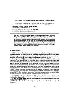
tion is crucial for the overall performance because if the processors compete between each other every time they fetch an instruction or (local) data, high performance can not be achieved. Local cache memories can be used in order to increase the performance of these systems. However, if cache memories are used for inter-processor data communication, cache coherence mechanisms has to be considered [3]. This introduces additional overhead limiting the overall performance. 2. MULTIPROCESSOR PLATFORMS In this section we give a brief description of our approach, described in [6], for building multiprocessor platforms. The multiprocessor platforms we consider are constructed by connecting Processing, Memory, and Communication components using Communication controllers (CC). Memory components are used to specify the processors’ local program and data memories and to specify data communication memories (CM) used to transfer data between the processors. The Communication components determine the communication network topology of a multiprocessor platform, e.g., a point-topoint network, a crossbar switch, or a shared bus. The Communication controller implements an interface between processing, memory, and communication components. We have developed a general approach to connect and synchronize programmable processors of arbitrary types via a communication component. Our approach is explained below using the example of a multiprocessor platform depicted in the right part of Figure 1 – see the non-shaded blocks. It contains several processors connected to a communication component (in this example – a crossbar switch CB) using communication memories (CMx’) and communication controllers (CCx’). The processors transfer data between each other through the CMx’ memories. A communication controller connects a communication memory to the data bus of the processor it belongs to and to a communication component. Each CC implements the processor’s local bus-based access protocol to the CM for write operations and the access to the communication component (CB) for read operations. In our approach each processor writes only to its local communication memory and uses the communication component only to read data from all other communication memories. Thus, memory contention is avoided. Each CM is organized as one or more FIFO buffers. We have chosen such organization because, then, the inter-processor synchronization in the platform can be implemented in a very simple and efficient way by blocking read/write operations on empty/full FIFO buffers located in the communication memory. The described communication mechanism and the usage of onchip memories for communication results in high performance of our multiprocessor systems. However, for some applications the memory requirements may exceed the available (on-chip) memory resources of the system. Therefore, we devised a mechanism and extended our platforms to support external memory for inter-processor data communication. The remaining part of the paper describes this mechanism and our interface for an external memory. 3. HIERARCHICAL MEMORY SYSTEM In this section we present our approach to use off-chip and on-chip memories, combined in a hierarchical memory system, for data communication between multiple processors in our platforms. An example of such platform is depicted in Figure 1. The hierarchical memory system is depicted in the left part of the figure – see the shaded blocks. For the sake of clarity the example contains only two proces-
uP1
CC1’
...
...
...
uP2
CC2’
CC2
CB
FIFO2’ FIFO1’’’
CM2
FIFOs
P/DM2
CM2’
Legend: uP − Microprocessor − Program and Data Memory P/DM − Communication Controller CC − Communication Memory CM − Crossbar CB EDM CTRL − External Data Memory Controller
FIFO1" FIFO2"
External Memory
Fig. 1. Example of a Multiprocessor Platform. nicate data only via FIFO buffers. Small size FIFOs are mapped onto on-chip memory CM 10 and CM 20 connected to a crossbar (CB ) or other communication component. Large size FIFOs are mapped onto the hierarchical memory system that includes on-chip SRAMs, i.e., communication memories CM 1 and CM 2 and an external (off-chip) memory. Mapping of large FIFOs is explained in the next section. External Data Memory Controller (EDM CTRL) manages the access to the external memory. Also, EDM CTRL is responsible for synchronizing and moving data between the SRAMs and the external memory using a Direct Memory Access (DMA) mechanism. Each processor has its own CM as a part of the hierarchical memory system (see the left part of Figure 1). The CMs are connected to communication controllers (CC1 and CC2). A CC allows multiple FIFOs to be mapped in a single CM and the CM to be accessed by the corresponding processor and EDM CTRL at the same time. The External Data Memory Controller and the CCs connect the on-chip CMs and the external memory in a particular way described in detail later in the paper. EDM CTRL acts as a single master (with CCs as slaves) that initiates data transfers between the CMs and the external memory. 3.1. Mapping FIFOs onto Hierarchical Memory System As explained above, the hierarchical memory system consists of low latency on-chip communication memories (CMs) and a large offchip memory. This memory system is used for mapping of large FIFO buffers as follows. For the sake of clarity assume that processors uP1 and uP2 (Figure 1) have to communicate data via large fifo buffers FIFO1 and FIFO2. Processor uP1 writes data to FIFO1 and reads data from FIFO2. Similarly, processor uP2 writes to FIFO2 and reads from FIFO1. In our approach each large fifo is split in three parts. For FIFO1, these are FIFO1’, FIFO1”, and FIFO1”’ as shown in Figure 2 (FIFO2 is split in the same way). Each CM FIFO1 FIFO1’
FIFO1’’
FIFO1’’’
size(FIFO1) = size(FIFO1’) + size(FIFO1’’) + size(FIFO1’’’) size(FIFO1’) = size(FIFO1’’’)