In-Line Multiport Calibration Algorithm Dylan F. Williams and David K. Walker National Institute of Standards and Technology, 325 Broadway, Boulder, CO 80303 Ph: [+1] (303)497-3138 Fax: [+1] (303)497-3122 E-mail:
[email protected] being used to connect the device under test to the analyzer, a unique termination impedance is applied to the unused probes. We begin the calibration and measurement procedure by connecting two-port in-line calibration standards between the west and east probes. We used this calibration to correct all the raw data taken by the analyzer to on-wafer measurement reference planes at the west and east ports. During the measurements of the thru line, we use the switches to disconnect first the west probe, and then the east probe, from the analyzer, and measure their imperfect on-wafer termination impedances. In the second step of the procedure, we connect the two-port calibration standards between the north and south ports. We used measurements taken in this configuration to determine four “error boxes” from a two-tier calibration procedure. These error boxes map measurements corrected to the west and east on-wafer reference planes to measurements corrected at the north and south on-wafer reference planes: they are uniquely
Abstract- We present a multiport measurement algorithm that uses only conventional in-line calibrations. The algorithm is well suited to performing on-wafer multiport measurements, and can correct with the thru-reflect-line calibration. We demonstrate the algorithm in a four-port measurement system.
INTRODUCTION We present a multiport calibration procedure based on conventional in-line two-port calibrations. This procedure allows on-wafer multiport measurements to be corrected by standard two-port calibrations, including the multiline thru-reflect-line (TRL) calibration [1]. It also reduces to an absolute minimum the number of connections made to the standards, requires only a set of six additional self-terminating switches to implement in a conventional wafer probing system, and fully corrects for imperfect termination impedances at all the measurement ports. The algorithm is similar to those proposed by [2] and [3], and is not limited to open-short-thru-load (OSLT) calibrations, as are the algorithms of [4] and [5]. In its current implementation, the algorithm can be used to perform four-port, three-port, and orthogonal two-port measurements, although extension to more than four ports is straight forward.
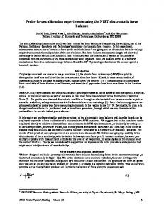
Port 1
Port 2
ANA
50
6
N
MULTIPORT CALIBRATION 50
6
The calibration corrects measurements made by the on-wafer probing system of Fig. 1, which consists of a conventional two-port network analyzer and six coaxial switches routing signals from port 1 of the analyzer to what we label the north, south, and west probes, and from port 2 of the analyzer to the north, south, and east probes. The system is arranged so that, when it is not
E
W S
50
6
50
6
Fig. 1.Four port measurement system schematic. Switches shown with port one of the analyzer connected to the south probe and port two connected to the north probe. The east and west probes are each terminated in 50 6.
Publication of the National Institute of Standards and Technology, not subject to copyright. 1
-20 Port 1 Port 2 2-port correction (west-east) 2-port correction (north-south) 4-port correction (west-east) 4-port correction (north-south)
0.05
Reflection coefficient (dB)
Transmission coefficient (dB)
0.10
0
-0.05
0
5
10
15
20
-40
-60
-80
25 26.5
Frequency (GHz)
Port 1 Port 2 2-port correction (west-east) 2-port correction (north-south) 4-port correction (west-east) 4-port correction (north-south)
0
5
10
15
20
25 26.5
Frequency (GHz)
Fig. 2. The transmission coefficients of our thru line measured as a two-port and a four-port. In order to measure the thru line as a four port we lifted the two unused probes off the substrate.
Fig. 3. The reflection coefficients of the thru line of Fig. 2.
port results in a straightforward way. However, the reference impedances of this four-by-four scattering matrix correspond to the imperfect termination impedances of the four probes, not 50 6. Once the four-by-four matrix is completely filled, we translate all its reference impedances back to 50 6 using the formulas in Appendix E of [6]. At this point we can assign port numbers to the east, west, north, and south reference planes, and the algorithm forms matrices of four-port, three-port, or two-port scattering and impedance parameters. The algorithm is also designed to construct differential even and odd mode parameters in its four-port correction mode.
determined because the switching network is passive and reciprocal. Again, during the measurements of the thru line, we also measure the imperfect termination impedances of the north and south probes. The final step of the procedure fills a four-by-four scattering parameter matrix for each multiport device with two-port measurement values with the procedure of [2]. Before adding these values to the matrix, we transformed the reference impedances of each set of 50 6 two-port measurements to the imperfect termination impedances of the two probes used to make them. This insures that the four-by-four scattering parameter matrix, whose reference impedances are equal to the four imperfect on-wafer termination impedances of the probes, is filled consistently. To illustrate the procedure, consider how we use a measurement made at the west and north reference planes to fill the corresponding elements of the four-byfour scattering parameter matrix. We first correct the raw two-port west-north measurement to the west and east reference planes. Then we apply an error box to port two of the partially corrected west-east data to transform it to a measurement corrected at the westnorth reference planes. Finally, we transform the reference impedances of this corrected 50 6 west-north measurement to the imperfect termination impedances of the west and north probes. Since all the measurements we add to the matrix have consistent reference impedances, this procedure allows us to fill the four-by-four matrix with the two-
MEASUREMENT EXAMPLE We demonstrated our system with the multiline TRL algorithm of [1]. The standards consisted of a 550 µm long coplanar waveguide (CPW) thru line, five longer lines of length 2.685 mm, 3.75 mm, 7.115 mm, 20.245 mm, and 40.55 mm, and two shorts offset 225 µm from the beginning of the line, all fabricated on a semi-insulating gallium arsenide substrate. The CPW had a center conductor width of 64 µm separated from two 261.5 µm wide ground planes by two 42 µm gaps. We moved the reference plane of the calibration to 25 µ m in front of the physical beginning of the lines and set the reference impedance to 50 6 with the method of [7]. Figures 2 and 3 compare conventional two-port measurements of the thru line we used in the calibration with measurements of the same thru line performed by 2
our calibrated four-port system. The figures show that the calibration procedure accounts for the imperfect termination impedances and properly corrects the data. The figures also show that the noise in the fourport measurements is comparable to the noise in the two-port measurements. Although not shown, our experiments indicated that the noise in the measurements can be reduced slightly by using one-tier calibrations to correct, when possible, the data measured at the north and south ports.
REFERENCES [1] R.B. Marks, “A Multiline Method of Network Analyzer Calibration,” IEEE Trans. Microwave Theory Tech., vol. 39, no. 7, pp. 1205-1215, July 1991. [2] J.C. Tippet and R.A. Speciale, “A rigorous technique for measuring the scattering matrix of a multiport device with a 2-port network analyzer,” IEEE Trans. Microwave Theory and Tech., vol. 30, no. 5, pp. 661-666, May 1982. [3] S. Sercu and L. Martens, “Characterizing n-port packages and interconnections with a 2-port network analyzer,” IEEE 6th Topical Meeting on Electrical Performance of Electronic Packaging Dig., pp. 163-166, Oct. 27-29, 1997. [4] F. Rérat, J. Carbonéro, G. Morin, and B. Cabon, “Automated measurement procedures of three-port and four-port devices on silicon,” 49th ARFTG Conf. Dig., pp. 122-131, June 13, 1997. [5] M. Schindler, P. Phillips, M. Fennelly, V. Adamian, and P. Enquist, “Characteristics and accuracy of a fully corrected four-port vector network analyzer,”50th ARFTG Conf. Dig., pp. 127-130, Dec. 4-5, 1997. [6] R.B. Marks and D.F. Williams, “A General Waveguide Circuit Theory,” J. Res. National Inst. Standards and Technol., vol. 97, no. 5, pp. 533-562, Sep.-Oct. 1992. [7] R.B. Marks and D.F. Williams, “Characteristic Impedance Determination using Propagation Constant Measurement,” IEEE Microwave Guided Wave Lett., vol. 1, no. 6, pp. 141-143, June 1991.
3