Integrated Direct Output Current Control Switching Converter using Symmetrically-Matched Self-Biased Current Sensors Yat-Hei Lam
Suet-Chui Koon
Wing-Hung Ki
Chi-Ying Tsui
Department of EEE Hong Kong University of Science & Technology Hong Kong SAR, China e-mail:
[email protected]
National Semiconductor Corporation Hong Kong SAR, China
Department of EEE Hong Kong University of Science & Technology Hong Kong SAR, China e-mail:
[email protected]
Department of EEE Hong Kong University of Science & Technology Hong Kong SAR, China e-mail:
[email protected]
e-mail:
[email protected]
Abstract -- A non-inverting flyback converter using an integrated symmetrically-matched self-biased current sensor was fabricated in a 0.35µm CMOS process. It operates in pseudo-continuous conduction mode and employs a direct output current control scheme to achieve excellent line transient response. The converter switches at 1MHz with an input of 1.2V to 2V to give an output of 1.5V and delivers 250mA. I. INTRODUCTION The controller of a DC-DC switching converter with voltage feedback is simple, but neither the inductor nor the output current is monitored, and the loop response is slow. Dynamic performance could be enhanced by employing current feedback, but slope compensation for the current loop is required to avoid sub-harmonic oscillation. Switching converters operating in the discontinuous conduction mode (DCM) do not exhibit sub-harmonic oscillation, because the inductor current starts from zero in every switching cycle. By raising the current floor to a non-zero value, the technique of pseudo-continuous conduction mode (PCCM) can be used to enhance the current handling capability [1]. The input voltage of a power converter with multiple sources changes from time to time, and spikes at the output are unavoidable. A control scheme that monitors and controls the output current directly may regulate the output voltage independent of the input voltage. In this paper, a direct output current control non-inverting flyback converter is proposed, and exhibits excellent rejection to abrupt line changes.
through the control loop. Therefore, the output current is directly controlled. If the input voltage changes suddenly, the ramp up slope in Phase 1 is changed. Yet, as both IPK and IFW are not changed in a time frame of one cycle, the shaded area in Phase 2 is not affected (Fig.1(b)). Hence, the output voltage is not disturbed by a sudden change in VIN, and excellent line transient response is achieved. III. CONTROL SCHEME IMPLEMENTATION The system block diagram of the proposed converter is shown in Fig.2. All switches are MOS transistors. The output voltage is scaled by a resistor string and compared to the reference voltage through a compensation circuit realized by an op-amp. The output of the error amplifier controls the peak inductor current. The functional block Logics & Drivers controls the switching sequence of the power stage. Inductor current information is extracted by sensing the current that passes through transistors MN1 and MN2 utilizing a MOS transistor scaling technique [2]. By sensing either MN1 or MN2, the inductor current can be sensed all the time. It should be noted that in Phase 3 when the inductor current is freewheeling, both MN1 and MN2 conduct, but MN2 is chosen to be sensed such that there is no hand-over problem at the start of Phase 1.
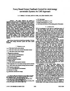
IV. SM SELF-BIASED CURRENT SENSOR A symmetrically-matched (SM) self-biased voltage mirror current sensor (Fig.3) [3, 4] is employed in the design. Using a time-multiplexing technique, the voltage-mirror core can be reconfigured in sensing both the switch and diode currents, and hence, the complete inductor current can be sensed without II. DIRECT OUTPUT CURRENT CONTROL CONVERTER additional loss. The voltage mirror core consists of M1A to M4A The proposed direct output current (DOC) control and M1B to M4B. Let switches SX2 and SY2 be closed, such that non-inverting flyback converter operates in PCCM is shown in the current of MN2 is sensed by MS2, with MN2 : MS2 = N : 1. Fig.1. The supply voltage VIN may vary from 2V down to 1.2V, Consider a large inductor current IL injected into MN2 at node while the converter maintains an output voltage at VOUT=1.5V. VSW2. With (W/L)1A = (W/L)1B, Id1A = Id1B are injected into M2A Every switching period is divided into three phases. In Phase 1, and M2B. Now, M2A, M2B : M4A, M4B = 1 : M, such that switches S1 and S3 are closed, charging the inductor at a rate of M2A+M4A are matched with M2B+M4B, and currents of di/dt=Vin/L, until it reaches the peak current IPK that is (M+1)Id2A are injected into MN2 and MS2. The matching forces controlled by the output of an error amplifier. In Phase 2, S2 VY to be equal to VX, thus achieving the voltage mirror and S4 are closed, discharging the inductor at di/dt=–Vout/L. function, and the current ratio IN2 : IS2 is N : 1, or IS2 = IL/(N–1). When the inductor current drops to the predefined This sensed current is mirrored by M5 for peak current control freewheeling level IFW, the converter enters Phase 3. In Phase 3, (using Rsen). The X branch and the Y branch are biased with S2 and S4 are closed, and the inductor current freewheels at IFW IL/(N–1), and hence, the larger the IL, the larger the bias current, until the period expires. The current flow is shown in Fig.1(a) and the faster the voltage mirror. The matching is so accurate and the inductor current waveform is shown in Fig.1(b). that even the large-signal analysis using MOS equation with Charge is delivered to the output in Phase 2 only, and the channel length modulation cannot reveal any difference average output current is proportional to the shaded area between the corresponding terminal voltages of any paired shown in Fig.1(b) that can be controlled by changing IPK transistors. Hence, the sensing accuracy surpasses all prior current sensors. For a sensing ratio of 1000 to 1, an inductor current of 1mA can be sensed accurately. By closing switches This research is in part supported by Research Grant Council CERG HKUST SX1 and SY1, the switch current of MN1 is sensed by MS1, and 6311/04E.
the same voltage mirror core is reused. Yet, the connections for MN1 and MN2 are different, as shown in Fig.3, because MN1 is sourcing while MN2 is sinking the inductor current. V. MEASUREMENT RESULTS The converter was fabricated and tested. Fig.4 shows the inductor current and the corresponding current sensor output voltage. Complete inductor current information was sensed and scaled accurately at a switching frequency of 1MHz. Fig.5 shows the line transient response. The supply voltage changed by 400mV but the output voltage showed no observable changes. Fig.6 shows the load transient response of the DOC control converter. The output voltage settled in 120µs when the load current changed from 50mA to 250mA, and 60µs when the load current changed from 250mA back to 50mA. VI. CONCLUSIONS A direct output current control scheme for switching converters in incorporating the current control loop with the pseudo-continuous conduction mode of operation was proposed. The DOC control converter was designed and demonstrated excellent line transient response. An accurate and fully-integrated current sensor is employed. The complete design was realized and verified by measurement results.
Fig.3 Symmetrically-matched self-biased current sensor
REFERENCES [1] D. Ma, W. H. Ki and C. Y. Tsui, "A Pseudo-CCM / DCM SIMO switching converter with freewheel switching", IEEE J. of Solid-State Ckts., vol.38, No.6, pp.1007-1014, June 2003. [2] Y. H. Lam, W. H. Ki and D. Ma, "Loop gain analysis and development of high-speed high–accuracy current sensors for switching converters," IEEE Int'l Symp. on Ckts. & Sys., pp.828-831, May 2004. [3] Y. H. Lam, W. H. Ki, C. Y. Tsui and D. Ma, "Integrated 0.9V charge-control switching converter with self-biased current sensor," IEEE Int'l Midwest Symp. on Ckts. & Sys., Hiroshima, Japan, pp.305–308, July 2004. [4] Y. H. Lam, W. H. Ki and C. Y. Tsui, "Symmetrically matched voltage mirrors and applications therefor," US Patent Application No. 11/185,294, July 20, 2005.
Fig.4 Measured inductor current and sensed current waveforms
Fig.5 Line transient response of DOC control converter
Fig.1 (a) PCCM flyback converter current flow and (b) corresponding inductor current waveforms
Fig.6 Load transient response of DOC control converter Die Size Technology Inductor Cout fswitch Vin Vout Max. Iout
Fig.2 System diagram of the non-inverting flyback converter
2.46mm × 2.82mm 0.35µm CMOS 4Metal-2Poly 4.7µH (off-chip) 47µF (off-chip) 1MHz 1.2V to 2V 1.5V 250mA
Fig.7 Converter specifications and chip micrograph