Integrated Siliam Systems, Malone Road, Belfast. * Cypress Irish Design Centre, Mahon Technology Park, Cork, Ireland. ** Edinburgh House .... 1. DG. SFG. FSgme 1. Regular processor design flow fix signal processing modules. Figare 2: ...
LOW-POWER SYNTHESIS FLOW FOR REGULAR PROCESSOR DESIGN R Woods', G Lightbody*, A Cassidy** G b e * * and J Spanier-
Abstract The paper presents the development of a low-power synthesis flow for the development of dedicated silicon circuits fbr data-dominated applications such as DSP systems. The work was carried out as part of a European ESPRIT low power action and a collaborative"low-power" project involving the universities of Liverpool, Manchester and Sheffield The design flow is briefly d e s m i and some results are presented for mult~~lier implementations and their use m the development of a Discrete Cosine Transform (DCT) circuit
1.
Introduction
In data-dominated applications, the performance capabilities of customized solutions are attractive particularly m applications such as video compression where functionality is fixed or has been standardized. For high volumes, customized VLSI solutions oft& the superior system performance m terms of both area and speed. For example, a processing performance of 100 GUPs/cm2Ws is achievable for computationally complex DSP algorithms m 0.35~standard cell CMOS technology. The performance gain comes fiom the process of developing an architecture that allows the algorithm to be efficientlymapped to hardware. This results m a very efficient solution as it is oRen possible to exploit characteristics of the algorithm m such a way to allow a highly optimised implementation to be realized There are a number of difkent design flows one of which is d e s m i d m this paper. The resulting designs are characterized by high area utilization, high levels of locality (preserving power) and efficient memory utilization. 2.
Low-power Regular Processors
Broadly speaking, DSP processor development canbe classified as two design styles. The first approach involves the development of an i"dJ-on set processor where suitable processing units are synthesized to achieve the required performance. Once a sensible the majority of the design activity is involved m architecture has been &t&ed, scheduling, memory o p t h i d o n and code transformation. As the underlying architecture is well understood and highly predictable, accurate power perfhmame is acbievable. The second approach attempts to synthesize an application specific architecture which closely matches the application fimctiomlity that it implements. This allows the designer to apply a number of performance efficient opthisations that would not be avajlable m the previous design flow. In addition, the designer bas access to hardware transfixmations and diffkent number systems which can o f k advantages m some applications. The material described in this paper concentrates on the synthesis of solutions which fall into the second classification and closely fdlows the work described m the book produced ftom this work'. This latter approach allows a mre power-efficient solution as the architecture can be customized to +Electrical and ElectronicEngineering, Queen's University of Belkt, Ashby Building, StranmillisRoad, Belfbst * Integrated Siliam Systems, Malone Road, Belfast
*Cypress Irish Design Centre, Mahon TechnologyPark, Cork, Ireland
** Edinburgh House, Cambridge, England +-I+ PCM-Siena, Vancover, Canada
12/1
Q 2001 The InSbiMion of Elechicai Engineers. Printed and p u b l i i by the IEE, Savoy Place, London WC2R 0% UK.
meet an area, speed and power budget. On the other hand, this f l e x i i i presents greater challenges
m delivering low power solutions as there are a greater number of degrees of fieedom. 3.
Low-Power design approach
Generally speaking, power reduction techniques either act to " k the switched capacitance (C*F) or trade off perfbrmance with reduced supply voltage2. In voltage " b a t i o n techniques, transfixmations are used to speed up the system's throughput beyond that which is necessary.The voltage is then reduced, slowing up performance until the required throughput rate is met but at a lower power consumption budget. However, in the semi-custom approach, the voltage of the technology is pre-determined by the silicon fiundry and cannot be altered by the user to reduce power. Typically, the voltage will have already been developed for low power operation and the user will access the design though h i phantoms which the user cannot m o w . Therefore, the "reduced voltage" techniques cannot be employed. Low power design therefbre must be targeted at reducing the switched capacitance. This is the summation of the products of the toggling o c d g on each node m the circuit by the capacitance of that node. It is important to consider switched capacitance as opposed to toggling or circuit capacitance dependently. For example, a circuit may have a large capacitative net which has a low switching activity and which will not contribute greatly to power c4"ption3. Conversely, low capacitance nets may have a lot of switching actm$. For these reasons, "i./ation of switched capacitance m order to reduce power consumptionis adopted for the regular processor meta flow. 4.
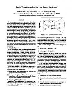
Regular Processor design flow for signal processing modules
The starting pomt of the regular processor 'beta" design flow is an algorithmic description of the functionality that has to be mapped to the processor. This algorithmic description is then refined using the design flow illushated m figure 1, resulting finally m a circuit level solution. The various stages are descriibedhere m more detail.
algorithmic: This involves the generation of a correct algorithmic description for the specific custom processor e.g. a full MPEG encoder. At this stage, the main focus is to develo and validate the algorithmic operation. High level modelling tools such as Cadence SPWl$ and Matlabm can be used to assist m this purpose.
data type refinement: At the algorithm stage, the development will have been carried out Using abstract data types, such as floating pomt arithmetic. In DSP design, a fixed pomt or a W e d range floating point solution is prefixable as it usually results m a more hardware efficient solutio= In many cases, the choice of fixed or floating point aritlrmetic is not straightforwad and can have a dramatic e m on the system pafkmnnce. This will include the considerationof W e wordlength issues such as truncation and saturation. task level: The algorithm is broken down into a number of separate tasks.For an MPEG encoder, the various tasks will inchxle the DCT and motion estimation. Typically, the h a l solution or the computationallycomplex parts of the system, will be implemented as a custom processor. A key issue is to ensure that the " a l n u m b e r of processors are used m the task allocation process. In a parameterizable Ip cores, the task allocation will have been pre-detexmined m the design process fir the core. psranel.array/data level issues: At this stage, the data parallel hctions will be transknmed into an underlying structure of processors. For DSP algoritbms, this d m v o h the
12/2
development of a VLSI architecture &om a Dependence Graph @G) representation. A considerable body of work exists into the transformation of commonly used functions such as the DCT and FFT into efficient structures where the number of multiplications and additions are reduced. A key issue will be an efficient use of hardware for the given application requirements. operatiodinstruction level issues: A number of choices are available at this stage including the structure of the processor blocks, arithmeticrepresentationand data control For example, the multipliers and adders can be implemented as separate processors or as a multiplyaccumulator structure. The choice of data type is highly important as the regular-processor designer has access to a wide choice of options e.g. fixed point and different types of arithmetic e.g. redundant arithmetic and residue arithmetic representations. The choice of the dif5xent arithmetic representations other than two’s complement, will be dictated by specific perfbrmance advantages gained. For example, redundant arithmetic can be used m the development of recursive structures such as recursive digital filters and m arithmetic functions that (arenatura& most significant bit k t , namely division and square root.
circuit level implementation involves preserving regularity in the generation of the circuit level descriptionand use ofp i p e h g registers m the datapath.
circuit level: The
Y=Bx
7 Algorithm
* Data Level
Validation
DG
Scheduling Inzerjhce development
1 Hardware -Ping High level timing
SFG
Arithmetic Cellfimctionality Insbuctbn level timing
I cirmt level
LoCali@ Circuit architecture
FSgme 1. Regular processor design flow fix signal processing modules 5.
Figare 2: Development ofVLSI architecture
Algorithmicissues
There have been a wide range of techniques fbr developing a mathematical ‘onfiom an algorithmic description. The process m figure 2 shows the general design flow fbr development of highly regular, VLSI solutions fix DSP algorithms. The initial specification is given as a mathematical relationship which is translated into a DG representation. A DG representation shows
12/3
the data dependencies between d i f k a t dataflows. At this stage, it is possiile to develop a Signal Flow Graph (SFG) qnmntah'on and a number of projections can be applied to develop SFG alternatives that match the algoritbmic requirements. The bit-level processors are then embedded mto the SFG. These may have detailed timing requirements which may mean retiming the SFG to ensure correct operation4. From a low power perspective, the fbal VLSI solution should ideally meet some or all ofthe following criterk Circuit representation with localized unmecti0115. Solution with efficient wordlengthrepresentations. 0
6.
optimized dataflow to "ketransitions on the internal circuit buses. Operatiodistruction level issues
At this stage m the design flow, the development of a candidate VLSI architecture Win have been chosen. A simple approach is to instantiate a processor fbr each ofthe processing elements. There are a variety of options open to the designer rangiug h m the arithmetic used for the instruction level processors to the choice of an operation level processor. Issues addressed at this level mchde: Choice of arithmetic style: This m c W s the use of alternative number systems such as redundant and residue arithmetic representations. Residue arithmetic works well m applications where word growth is limited. Redundant arithmetic has particular low power advantages m that it breaks carry propagation chains m addition and therefbre multiplication. This reduces the circuit switching. Detailed architecture of the instruction level processor: A hierarchical approach based on simple, processors can be used. Alternatively, it is possible to develop the circuit architecture using, for example, the Co-ordinate Rotation Digital Computer (CORDIC)transformation. The choice of bit level circuit architecture can also impact power performance. 7.
Power Estimation of Processor Block
A mnnber of studies have been carried out into adders structure^^*^ and multiplier structures3. Some of these results are shown m table 1. The rrmltrplier strudures presented all have different capabjlities e.g. the Wallace-Tree structure can operate at much higher hquencies than the anay structures. This factor was taken into consideration. The table clearly shows that preserving hierarchy at the circuit level allows a power saving. This is particularly observable at higher wordlengths where the increased wordlengths result m many more longer nets which make have a greater @act on power consumption.
8.
AppIication to 1D DCT example
The DCT is a key DSP hction that has been used extensively jkr image processing and some speech coding applications.The 2D version of the DCT is a separable hction that can be split mto two single DCT functions. This approach is commonly termed r o w - c o h decomposition. One approach to the implementation of the 1D DCT is to transfbrm the expression into a transfkr function resembling a second order IfR filter repmentation*.This gives a circuit comprkihg two multipliers and three adders which can be used to develop DCT m i p. fix a wide range of specifications.An~ghasbeencarriedoutonacircuitwitha8bit~~11 bitoutputanda12
bit mtemal datapath and that operates at 100 MHZ. The two multipliers have coefficient wordlengths of 12 bits and 10 bits. Name Carry-Save array multiplier6 synthesized as an array Carry-Save amy multiplier6with no layout hierarchy Two’sComDlement Booth Encoded Wallace Tree
8-Bit(m7N) 5.99 3.23 4.00
16-bit(mW) 23.19 25.94 32.24
24-bit(mW) 56.92 67.96 86.12
Table 1. Power consumption of multipliers processmg random data at 20Ivl.H~
A number of approaches were investigated The hierarchical approach involved the derivation of a solution where the mdividual processing blocks multipliers and adders are synthesized and implemented mdividually. An approach usmg carry-save d i l i e r s was investigated where the circuit layout is generated without imposing any hierarchy ie. fiat. A hierarchical DCT approach usmg carry-save multipliers was also mvestigated. These results are shown m table 2.
I
I OIlginal DCT system (Wallace Tree)
HierarchicalDCT system(Carry-save)
Power(mW 64.7 58.9 49.0 44.0
I
Table 2. Power consumption ofmultipliers procesSing random data at 20MHz 9.
Conclusions
In this paper, a brief description of a low-power design flow has been presented. It is shown how a low-power design approach is achievable at an algoritldarchitectural level without resorting to Circuit or technology level techniques. Future works aims to target a design at each stage of the design flow to demonstrate more fully the design gains possible as the DCT exampIe only demonstrates the impact at the operatiodkutmctionaland circuit levels.
10. References 1. E ~ sF Cathor
m),
dti-media and telecom “Udid 1 m - w design flow for data applications”,KhnvaAcadanicpublishgs,~us&2o0o. 2. A -C S. Shag, and R. Brodersen, R, “Low Power CMOS Digital Design”, IEEE Journal of Solid-state Circuits,VOL27, NO.4,1992, pp473-484. 3. G. b e , J. R Spanier, and R Woods, ’”V-Power design of Signal Processing systems using characterization of silicon IP cores”, 3326~silamarc o n ~ m c eon Signals, systems and computers, A d m yUSA, Oct. 1999, invitedpm, lEEE Computer SocietY, ~~767-771. 4. D T”r, R F Woods and J VhWaxmy, “Architecaaal Sydlesis of Digi!al signal processing Algo&ms Using “lRIS”’’, Journal OfVLSI SI@ procesSmg,Vol. 16, NO1, May 1997, pP41-56. 5. A M. Shams and M. Bayoumi, “A Structured approach for Designing Low Power Adders”, 31st hilomar Cdaence on Signals, Systems and Computers, lEEE Computer Society, Vol. l., 1997, pp 757-761. 6. C. Nagendra, M-J.Irwin,and R M. Owens,R-M. “Area-TimePowerTradeof&in Parallel Adders”, IEEE TransactianS011 Circuits and Swm,VOL43, NO.10,1996, ~689-702. 7.J. Deverell,“PipelinedIterative Arithmetic arrays” IEEE Trans.On Cumputers, C-241,1975, pp 317-322. 8. J. Hunter,“Rapid Design of Discrete Cosme Transform Cores for Multimedia VLSI Systems”, PhD thesis, The Queen’s UnivepSityof Belfast 1999. 9. Spanier, J., Keane, G. and Woods R,“Low Power Implementaticm of a Discrete Cosine Transform IP core” Proceedings of the Deign, Automation and Test in Europe Cbnfmence (DATE2000), Paris, France, 27-30 March 2000, Date User Forum, Session8C, pp. 267-271.