flops and en2 is connected to the last four flip-flops. If en. = â1â, then the respective half of the flip flops to which the en signal is connected will be in active mode.
ISSN (Online) 2321 – 2004 ISSN (Print) 2321 – 5526
INTERNATIONAL JOURNAL OF INNOVATIVE RESEARCH IN ELECTRICAL, ELECTRONICS, INSTRUMENTATION AND CONTROL ENGINEERING Vol. 2, Issue 9, September 2014
LOW-TRANSITION TEST PATTERN GENERATION FOR MINIMIZING TEST POWER IN VLSI CIRCUITS USING BIST TECHNIQUE Praveen J1, MN. Shanmukhaswamy2 Department of Electronics and Communication, J.S.S. research foundation, Mysore University, Mysore, India 1 Department of Electronics and Communication, J.S.S. research foundation, Mysore University, Mysore, India 2 Abstract: Any Integrated circuit (IC) manufactured by the semiconductor manufacturing company contains test circuit and the circuit under test (CUT). The test circuit is used to test the correct functionality of the CUT and which is called Built In Self Test (BIST). This Built In Self Test used to generate test vectors which are applied to the circuit under test by inbuilt chip within an integrated circuit. In pseudorandom BIST design, the test vectors are generated in random style by Linear Feedback Shift Registers (LFSR). The main drawback of these conventional LFSRs is, it generates normally a number of random natured test vectors for testing the CUT in which many are repeated vectors and application of which unnecessarily increase the test power without contributing much to the fault coverage also the bulkiness of the CUT increases. This paper presents a new approach, called Low Power -Bit complement test vector generation technique (LP-BCTVG). In LP-BCTVG technique, the output bits are complemented due to which unreported test vectors are increasing also by which better fault coverage with a reduction in the bulkiness of the test circuit can be achieved. Keywords - Low power- Bit complement Test vector Generation (LP- BCVPG), Bulkiness, test power and Linear feedback shift register (LFSR) 1. INTRODUCTION Today‟s System-On-Chip (SOC) devices contain an integration of a large number of processors, different types of memories like SRAM, user defined logic and Digital signal processors, with an increasing count in transistors on a single chip thereby, challenging the design and testing methodologies in vogue. The testing of ICs, today mandates a new and high-level of competence and accuracy, expecting complete verification through all of the stages of the design process. It is well-known fact that power dissipation in the circuit during the test mode is considerable more compared to that in the normal mode [1]. This can be admitted to the correlation existing between consecutive test vectors applied during the normal mode of operation of the circuit.But, this is not the fact in the test mode. There is no considerable coefficient of correlation between successive vectors in the test mode. This automatically means that the primary switching activities will be more in the test mode compared to that in the normal mode and the power dissipation will be higher in the test mode. Thus, more the transitions between the test vectors more will be the power dissipated. Hence, low power testing is the need of the hour. By using BIST test design this can be easily overcome. A BIST design consists as a part of the target device that aids in the confirmation of the internal functionality of the exacting design for which it is assigned. BIST is a technique of allowing test logic to be integrated with die itself. Copyright to IJIREEICE
The BIST architecture is widely accepted because of its very many advantages like the reduction in test application time, reduction in the cost of generation of test vectors, to allow at-speed testing, to provide an alternative to the expensive Automatic Testing Equipment (ATE) and the reduction in the volume of test data. Also, the overhead area occupied by the BIST in the circuit can be considered negligible in comparison to the size of the target system [2]. The BIST makes the target system independent of any external automatic equipment for testing [1]. Hence, this proposed method aims to analyze and discuss a circuit that generates test patterns that help reduce the average and peak power dissipation in BIST architecture during testing mode. Also, efforts are made to bring about appropriate modifications to the logical and structural implementation, of the circuit under consideration, in order to reduce the power dissipation even further. 2.
TEST PATTERN GENERATION
The vectors in the test mode may consume higher average or peak power than that in the normal mode. The decreased coefficient correlation between the pseudorandom patterns (the patterns generated will repeat after a cycle is completed) generated by the LFSR is credited as the reason for the additional dissipated power in test mode. This in turn ends in an increase in the switching actions of the circuit, thereby, causes to increased power dissipation [1]. www.ijireeice.com
2027
ISSN (Online) 2321 – 2004 ISSN (Print) 2321 – 5526
INTERNATIONAL JOURNAL OF INNOVATIVE RESEARCH IN ELECTRICAL, ELECTRONICS, INSTRUMENTATION AND CONTROL ENGINEERING Vol. 2, Issue 9, September 2014
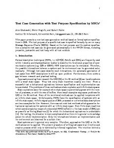
Figure1: Conventional Linear feedback shift register (LFSR)
2.1 Need for low power testing The System-On-Chips platform imposes a challenge in the design and testing methodology. Testing gains the primary significance in terms of issues and expenditure, thereby, demanding a wide range of possible novelties. The area of concentration, here, is power dissipation [1]. In general, the power consumed during the test mode is more than that in the normal mode of operation. This additional power dissipated may pose a threat to the circuitry and can also lead to a breakdown of the chip. This in turns will raise the costs, increase the difficulty in verifying the performance of the circuit and thereby reduce the final code [1]. Having learnt the above, the necessity of decreasing the power dissipated in a circuit during the test mode is a major milestone for further advancements in VLSI design. A number of reasons can be quoted for the increased power consumption in the circuit during the test mode [2]. Decreased correlation between the test vectors can be sited as the first reason. Normally, a considerable correlation exists between the inputs during the operational mode, but may not be the same in the test mode. This decreased correlation in the input during the test mode increases the switching activities, thereby increasing the power dissipation [1]. Secondly, the use of parallel testing process by test engineers in order to reduce the test application time can result in increased power dissipation. The third reason can be attributed to the DFT circuit that is inbuilt in the design for the test mode, which is normally idle during the operational mode, however, is extensively active in the test mode [2]. 2.2 Reviews of Low Power BIST Models The low power BIST issue can be tackled by designing a DFT using various techniques. The increase in the number of components and functional units in a single chip automatically means an increase in the testing difficulties. Described below a few methods designed to tackle and reduce the power dissipation during test mode. Dual speed LFSR (DS-LFSR) is the proposed model in [5] which aids in decreasing the heat dissipated during the test process. Here, two LFSR‟s, a slow LFSR and a normal speed LFSR are used. A slower clock speed is used for the slow LFSR compared to that of the normal speed LFSR. This reduces the transition density at the inputs which, in turn, Copyright to IJIREEICE
reduces the heat dissipation. The increase in the number of vectors accomplishes increased fault coverage proportion by generating patterns that are distinctive and evenly distributed. Also, further heat dissipation is reduced by combining compatible inputs with the inputs of slow LFSR in order to increase the number of inputs. In the method adopted in [6], a test - per - clock architecture model is designed which modifies the conventional LFSR to generate low power patterns. In this scheme, two clocks, which are in synchronies with a Master clock, are used. Both clocks have a speed that is half of that of a normal clock speed. During one clock cycle, one of the clocks is used to activate one half of the D flip flops and for the next clock cycle, the other clock is used to activate the second half of the D flip flops. The same management is executed for the clock that feeds the Test Pattern Generator as well. The fault coverage and the testing time remain the same as that of a standard BIST model and the area overhead is almost negligible. The test pattern generator algorithm described in [7] is the Non-Linear Hybrid Cellular automata for testing, based on Cellular Automata for reducing power dissipation and increasing fault coverage ratio at the same time. Here again, the test – per – clock design has been adopted, wherein, the main outputs are monitored by an Output Data Analyzer (ODA) and the primary inputs are fed by a Hybrid Cellular Automaton (HCA). The Cellular Automata generates low power test vectors. This model proposes two main goals; namely, to reduce power dissipation during the test mode and give the required fault coverage ratio for the respective test patterns. However, the area overhead remains the same as for a normal BIST architecture. Because of the good statistical properties, the Cellular Automata scheme is considered a very attractive option for Test Pattern Generation [14]. The BIST model designed in [8] is a scheduling process of the BIST that considers constraints like the power dissipation, area overhead, noise, etc. That implements the BIST architecture with a highly modular architecture and thereby, introduces a new BIST control methodology. The BIST scheme and the BIST control elements are independent of each other because of the uniformity of the interface. For the Power dissipation Analysis, the clock speed is considered at the normal system clock speed to obtain all of the advantages, though a clock speed lower than the system speed will prevent excessive power www.ijireeice.com
2028
ISSN (Online) 2321 – 2004 ISSN (Print) 2321 – 5526
INTERNATIONAL JOURNAL OF INNOVATIVE RESEARCH IN ELECTRICAL, ELECTRONICS, INSTRUMENTATION AND CONTROL ENGINEERING Vol. 2, Issue 9, September 2014
dissipation due to the increased activity rate. Also, of test patterns and also achieves the required span of fault optimization is achieved by sharing the BIST strategy with coverage allowing testing at system speed. Also, a mixed other groups of the same type that are actually identical solution depending on the reseeding scheme and the test but may have their parameters differ. vector inhibiting technique is put forward to handle The Low Power/Energy BIST scheme for Data paths difficult – to – test circuits that include pseudorandom designed in [9] is proposed based on the fact that power resistant faults. This test permits a test sequence of consumption by functional modules, like multipliers, of acceptable length along with lower Weighted Switching the datapath is huge. Hence, a Low Power BIST Activity in a circuit. architecture for data paths created along the multiplier – In the paper discussed in [12], a low power BIST design accumulator pairs are considered. This model relies on test based on the pre-computation architecture is intended. In a patterns that are deterministic. In this case, two schemes standard BIST architecture, the LFSR or a Cellular are proposed, wherein, one relies on reduced power Automata is used to generate the test patterns. A subset of dissipation during the BIST procedure and the other relies these patterns then applies to the Circuit Under Test and on reduced power dissipation between consecutive test the outputs from the Circuit Under Test are analyzed by an patterns. The former scheme depends on compact test Output data Analyzer (ODA). The patterns generated by patterns generated by a counter – based Test Pattern the source contain vectors to obtain the required fault Generator which is of fixed size. This causes a very low coverage and also those vectors that do not contribute to primary input switching activity, which in turn lower the the fault coverage. Because each test pattern applied to the energy consumption. Since the area overhead and the Circuit Under Test consumes energy, power consumption efficiency are far better, it is much compatible and is reduced by removing those test vectors which do not effective with portable devices. The latter scheme depends contribute to the fault coverage. This project devises on the linear – sized test patterns and is highly reliable in various methods to identify that subset by approximating reducing average energy consumption among test vectors. the energy consumed by each pattern with a constant Search depending on genetic algorithm, in order value. This approximation enables in reducing the issue of establishes signal probabilities, to decrease power finding the subset T with minimum power dissipation. consumption, called the POWETEST, is modeled in [10]. This model targets for portable and wireless applications, where power consumption is the primary concern. A random pattern generation using weighted average is the mode of operation here. The procedure depends on controllability and observability measure depending on the probability that the main input signal is logic „1‟ and this aids the testability of a circuit. The relevant inputs to the primary node are provided either by an LFSR or a Cellular Automata. Controllability is a measure of the difficulty of setting a particular node to a logic „1‟ or logic „0‟ from the primary input and Observability is a measure of difficulty in observing a particular node from the primary output. The test vector inhibiting technique in [11] helps in reduced power dissipation by generating the least number 3. LP - Bit complement test vector generation technique (LP-BCTVG)
Copyright to IJIREEICE
www.ijireeice.com
2029
ISSN (Online) 2321 – 2004 ISSN (Print) 2321 – 5526
INTERNATIONAL JOURNAL OF INNOVATIVE RESEARCH IN ELECTRICAL, ELECTRONICS, INSTRUMENTATION AND CONTROL ENGINEERING Vol. 2, Issue 9, September 2014
Figure 2: Proposed LP-BCTVG The conventional LFSR generates a less number of test patterns in which most of the test pattern is repeated, which causes excessive dynamic power dissipation by increasing the switching activities when they are applied to any benchmark circuits (CUT). In order to overcome the excessive switching activities, the patterns need to be generated in such a way that two successive patterns should have a high correlation. This can be achieved by placing the logic which generates low power patterns within LFSR-BCTVG proposed in Figure2. Hence, the minimization of switching activities within CUT along with the reduction of bulkiness of the test circuit can be achieved by using the pattern generating logic shown in Figure2. To meet both the requirements, the Bit complementing technique is being used with R-injector and multiplexer logic as shown in Figure2. The circuit shown in Figure3 is the LP-BCTVG, which is designed by integrating the bit complementing logic with the R-injector and multiplexer logic, which are being used to generate the patterns with high correlation to decrease the switching activities and thus, the dynamic power dissipation. R-Injection circuit – The R-Injection circuit shown in figure 4. Consists of an AND gate, an OR gate and a 2*1 multiplexer. The R-Injection circuit holds the current state and the next state of the corresponding
Copyright to IJIREEICE
bits of each vector. When both the corresponding bits are equal, the AND and the OR gate generates the same value of the bit. However, when the corresponding bits are not equal, the random bit R is given to the output. Multiplexer – As is known, it consists of two AND gates and an OR gate. The inputs to one of the AND gates are sel signal and the output of the corresponding R-Injection circuit. The other AND gate gets its inputs as sel BAR and the output of the corresponding flip-flop. The output of the AND gate is then ORed to give the final output. The random vectors are generated with the help of two enable signals (en1 & en2) and two select signals (sel1 & sel2) which are not dependent on the size or the polynomial of the LFSR. Signal Sel1 is connected to the first four multiplexers and signal Sel2 is connected to the last four multiplexers. The Sel signal selects either the output of the flop or the output of the R-Injection circuit accordingly. If Sel = „1‟, then the flop outputs are directly connected to the LP-BCTVG circuit Outputs and if Sel = „0‟, then the R-Injection circuit‟s outputs are connected to the LP-BCTVG circuit Output. Similarly, signal en1 is connected to the first four flipflops and en2 is connected to the last four flip-flops. If en = „1‟, then the respective half of the flip flops to which the en signal is connected will be in active mode. In active mode, every flop assigns its input status to its output pin. However, if en = „0‟, the half of
www.ijireeice.com
2030
ISSN (Online) 2321 – 2004 ISSN (Print) 2321 – 5526
INTERNATIONAL JOURNAL OF INNOVATIVE RESEARCH IN ELECTRICAL, ELECTRONICS, INSTRUMENTATION AND CONTROL ENGINEERING Vol. 2, Issue 9, September 2014
Table 1 Clk
Pattern
en1en2 sel1sel2
1
Pi
1 0
1 1
1010 1011 1010 1011
2
Pk1
0 0
1 0
1010 1111 1010 1111
3
Pk2
0 1
1 1
1010 0101 1010 0101
0 0
0 1
1 0
1 1
4 5
Pk3 Pi+1
the flip flops to which the signal is connected will be in the idle mode. In idle mode, every flop will not shift the input status to its output pin and instead, they retain the previous value. The circuit also consists of the clock and the Test_en signal that uses the select the Test mode. Table 1. Shows the intermediate test vectors generated based on a seed value. Referring to the Figure3 LP-BCTVG circuit, the „first part flops‟ (before the dummy block) are ff1, ff2, ff3, ff4, ff5, ff6, ff7 and ff8. Also, the „second part flops‟ (after the dummy block) are ff9, ff10, ff11, ff12, ff13, ff14, ff15, ff16. Step 1: en1=1, en2 = 0, sel1=1, sel2 = 1 As en1=1, the first part flops will be in active mode. As en2=0, the second part flops will be in idle mode. As se1=1 and sel2=1, all the output pins of LP-BCTVG circuit (O1, O2, O3, O4, O5, O6, O7, O8, O9, 010, O11, O12, O13, O14, O15 and O16) will be directly driven by the output pin of respective flops by bypassing the R-inject logic. Step 2: en1=0, en2 = 0, sel1=1, sel2 = 0 As en1=0 and en2 =0, both part of the flip flop will be in idle mode. As se1=1 and sel2=0, only (O1, O2, O3, O4, O5, O6, O7, and O8) output pins of LP-BCTVG circuit will be directly driven by the output pin of respective flops by bypassing the R-inject logic. But from (O9, 010, O11, O12, O13, O14, O15 and O16) circuit will be driven by passing through R-inject logic, which insert a bit (O or 1) into the output pins of LP-BCTVG. Step 3: en1=0, en2 = 1, sel1=1, sel=1 As en1=0, the first part flops will be in idle mode. As en2=1, the second part flops will be in active mode. As se1=1 and sel2=1, all the output pins of LP-BCTVG circuit (O1, O2, O3, O4, O5, O6, O7, O8, O9, 010, O11, O12, O13, O14, O15 and O16) will be directly driven by the output pin of respective flops by bypassing the R-inject logic. Step 4: en1=0, en2 =0, sel1=0, sel2 =1 As en1=0 and en2 =0, both part of the flip flop will be in idle mode. As se1=0 and sel2=1, then (O1, O2, O3, O4, O5, O6, O7, and O8) circuit will be driven by Copyright to IJIREEICE
LP-BCTVG
1111 0101 1111 0101 0101 0101 0101 0101
passing through R-inject logic which insert a bit (O or 1) into the output pins of LP-BCTVG. But (O9, 010, O11, O12, O13, O14, O15 and O16) output pins of LP-BCTVG circuit will be directly driven by the output pin of respective flops by bypassing the R-inject logic. Step 5: The procedure as in step 1 is repeated here and vector Pi+1 is generated. The above method continues from step 1 through step 5 for as many clock cycles as is required. The complete circuit is controlled by a finite state machine (FSM), as is shown in the below circuit that acts as the gear stick in the generation of the test patterns. The FSM serves as the control unit for the generation of the test patterns by continuing through steps 1 to 4. The inputs to the FSM are test_en and clk. When test_en = 1, the FSM is initiated with step 1 wherein en1 en2 = 10 and sel1 sel2 = 11 and continues till step 4 with the generation of a vector for every clock pulse. As we can be observe, the intermediary vectors Pk1, Pk2 and Pk3 are generated between two consecutive random vectors P1 and P2. It is seen that the number of transitions between P1 and P2 are 7. However, the transitions between P1 & Pk1 = 1, Pk1 & Pk2 = 2, Pk2 and Pk3 = 2 and that between Pk3 and P2 = 2. This shows that the correlation between two successive test vectors being significantly reduced after the introduction of the three intermediary vectors which reduces power dissipation within CUT by minimizing the switching activities.
4. EXPERIMENTAL RESULTS The test patterns generated by LFSR and LP-BCTVG are shown in table 3 is used for verifying the ISCA85 benchmark circuit C17, S27 and S289. Simulation and synthesis are done in Xilinx 14.1 and switching power is carried out of table 2 is done using Spy Glass. Programming of the design is done in Verilog and simulation of the design is carried out using MODEL SIM 6.2.
www.ijireeice.com
2031
ISSN (Online) 2321 – 2004 ISSN (Print) 2321 – 5526
INTERNATIONAL JOURNAL OF INNOVATIVE RESEARCH IN ELECTRICAL, ELECTRONICS, INSTRUMENTATION AND CONTROL ENGINEERING Vol. 2, Issue 9, September 2014
Table 2 Circuit Under Test ( CUT) 32-bit LFSR Leakage Power Internal Power Switching Power Total Power
Proposed LPD-BCTPG
C17
S27
S298
C17
S27
S298
2.19nW
3.84nW
29.45nW
2.22nW
3.95nW
29.516nW
195.86nW
258.16nW
357.20nW
177.32nW
189.11nW
428.09nW
104.19nW
417.12nW
860.03nW
40.35nW
68.79nW
1.18uW
302.25nW
679.128nW
1.24uW
219.90nW
261.87nW
1.64uW
Table 2 shows the Switching power dissipation of the concluded that low power Bit complement test pattern 32bit Conventional LFSR. The test patterns which are generation (LP-BCTVG) is very much useful for power generated from this 32bit Conventional LFSR are applied optimization in BIST. to the three different 32bit benchmark circuits C17, S27 and S298. 6. FAULT COVERAGE The test patterns generated by LFSR, LP-BCTVG and LPBITPG are shown in table 5, table 6 and table 7 are used for verifying the ISCA85 benchmark circuit C17, S27 and S298. Simulation and synthesis are done in Xilinx 14.1 and power analysis is done using Spy Glass. Programming of the design is done in Verilog and simulation of the design is carried out using MODEL SIM 6.2.
5. COMPRESSION RESULT From Table 2 experimental results shows that Switch power dissipation of the benchmarks circuit C17 for proposed LP-BCTVG indicate up to 61.27% reduction in switching power compare to conventional LFSR, similarly S27reduction in 83.50% and S298 reduction of 86.27%. It is
Table 3 Circuit Under Test ( CUT) 32-bit LFSR
Proposed LP-BCTVG
C17
S27
S298
C17
S27
S298
65536
65536
65536
65536
65536
65536
65058
65050
65536
65529
65038
65529
No. of repeated test pattern
500
486
494
493
498
498
No. of gates
192
192
192
294
294
294
Fault Coverage (% )
99.23
99.25
99.24
99.24
99.24
99.24
Expected Patterns for 16- bit No. of Non repeated test pattern
Copyright to IJIREEICE
www.ijireeice.com
2032
ISSN (Online) 2321 – 2004 ISSN (Print) 2321 – 5526
INTERNATIONAL JOURNAL OF INNOVATIVE RESEARCH IN ELECTRICAL, ELECTRONICS, INSTRUMENTATION AND CONTROL ENGINEERING Vol. 2, Issue 9, September 2014
From Table 5 experimental results of Benchmark circuit conventional LFSR. In proposed LP-BCTVG, fault C17 show that fault coverage is decreased to 99. 23 % in coverage increased to 99.98 % compare to conventional proposed LFSR-BCTVG compare to conventional LFSR LFSR. but the number of gates required to design testing circuit is decreased to 50 % hence bulkiness of the chip is decreased almost half of the
Copyright to IJIREEICE
www.ijireeice.com
2033
ISSN (Online) 2321 – 2004 ISSN (Print) 2321 – 5526
INTERNATIONAL JOURNAL OF INNOVATIVE RESEARCH IN ELECTRICAL, ELECTRONICS, INSTRUMENTATION AND CONTROL ENGINEERING Vol. 2, Issue 9, September 2014
7. CONCLUSIONS This paper presents a new Low Power Bit complement test pattern generator technique (LT-BCTPG). Power consumption of LT-BCTPG is reduced due to the bit Complement technique and also the bulkiness of the circuit is reduced to half of the conventional LFSR. LTBCTPG provides greater randomness than Conventional LFSR and also which have the potential to generate all possible test patterns to detect all possible faults. The switching activity in the CUT power consumption is reduced by increasing the correlation between patterns and also within each pattern.
[9] Xiaodong Zhang, Roy K, Bhawmik S. “POWERTEST: a tool for energy conscious weighted random pattern testing” VLSI Design, 1999. Proceedings. Twelfth International Conference On 7-10 Jan. 1999 Page(s):416 - 422 [10] Girard P, Guiller , Landrault C, Pravossoudovitch S, “A test vector inhibiting technique for low energy BIST design”. VLSI Test Symposium, 1999. Proceedings. 17th IEEE 25-29 April 1999 Page(s):407 - 412 [11] Corno F. Rebaudengo M. Reorda M.S. Violante M., “A new BIST architecture for low power circuits” Test Workshop 1999. Proceedings. European 25-28 May 1999 Page(s):160 – 164. [12] P. D. Hortensius, R.D. McLeod, W. Pries, D. Michael Miller, H.C. Card, “Cellular Automata-Based Pseudorandom Number Generators for Built-In Self Test”, IEEE Transaction in CAD, Vol. 8, No. 8, August 1989, pp.842 – 859.
8. REFERENCES [1] N. Ahmed, M. H. Tehranipour, M. Nourani, “Low Power Pattern Generation for BIST Architecture”, IEEE Circuits and Systems, 2004. ISCAS '04. Proceedings of the 2004 International Symposium, 23-26 May 2004, Vol. 2, pages 689-92. [2] Girard P. “Survey of low-power testing of VLSI circuits”, Design & Test of Computers, IEEE Volume 19, Issue 3, May-June 2002 Page(s):80 - 90 [3] John Koeter. Texas Instruments. SCTA036A, December 1996. “What‟s an LFSR?” [4] Seongmoon Wang, Gupta, S.K. “DS-LFSR: a new BIST TPG for low heat dissipation”, Test Conference, 1997. Proceedings. International 1-6 Nov. 1997 Page(s):848 – 857. [5] Girard P, Guiller L, Landrault C, Pravossoudovitch S, Wunderlich H.J. “A modified clock scheme for a low power BIST test pattern generator”. VLSI Test Symposium, 19th IEEE Proceedings on. VTS 2001 29 April-3 May 2001 Page(s):306 – 311. [6] Corno F. Rebaudengo M, Reorda, M.S, Squillero G, Violante M, “Low power BIST via non-linear hybrid cellular automata”. VLSI Test Symposium, 2000. Proceedings. 18th IEEE 30 April-4 May 2000 Page(s):29 – 34. [7] Zorian Y. “A distributed BIST control scheme for complex VLSI devices”. VLSI Test Symposium, 1993. Digest of Papers. Eleventh Annual 1993 IEEE 6-8 April 1993 Pages4 – 9. [8] Gizopoulos D, Krantitis N, Paschalis A, Psarakis, Zorian Y. “Low power/energy BIST scheme for data paths”, VLSI Test Symposium, 2000. Proceedings. 18th IEEE 30 April-4 May 2000 Page(s):23 - 28
Copyright to IJIREEICE
BIOGRAPHIES Mr. Praveen J. Completed his B.E degree in Electrical and Electronics from Kuvempu university in the year 1999,M.Tech in VLSI design and Embedded system in the year 2004 and currently pursuing his Ph.D Degree in Electronics from Mysore University, Karnataka from 2010. He is presently working as an Associate Professor in the Department of Electronics and communication, Alva‟s Institute of Engineering & Technology, Moodbidri, South Canara. Karnataka, India. His areas of interest are VLSI Design and Testing. He has published two papers in the International Journals and Con fer en ces in his field of expertise. He h a s delivered invited lectures and organized a few in-house workshops and certificate programs.
www.ijireeice.com
2034
ISSN (Online) 2321 – 2004 ISSN (Print) 2321 – 5526
INTERNATIONAL JOURNAL OF INNOVATIVE RESEARCH IN ELECTRICAL, ELECTRONICS, INSTRUMENTATION AND CONTROL ENGINEERING Vol. 2, Issue 9, September 2014
Dr. M. N. Shanmukha Swamy completed his B.E. degree in Electronics and Communication Mysore University in the year 1978, M.Tech in Industrial Electronics from the same university in the year 1987 and obtained his Ph.D in the field of Composite materials from Indian Institute of Science, Bangalore in 1997. He is presently working as Professor in the Department of Electronics and communication, Sri Jayachamarajendra college of Engineering, Mysore, Karnataka, India. He is guiding several research scholars and has published many books & papers both in National & International conferences & journals. His research area includes Wireless Sensor Networks, Biometrics, VLSI and composite materials for application in electronics.
Copyright to IJIREEICE
www.ijireeice.com
2035