J. Mater. Sci. Technol., 2010, 26(1), 87-92.
Microstructure and Mechanical Properties of Nanocrystalline Tungsten Thin Films H.L. Sun, Z.X. Song, D.G. Guo, F. Ma and K.W. Xu† State Key Laboratory for Mechanical Behavior of Materials, School of Materials Science and Engineering, Xi0 an Jiaotong University, Xi0 an 710049, China [Manuscript received September 16, 2008, in revised form January 22, 2009]
Tungsten (W) thin films were prepared by magnetron sputtering onto Si (100) substrates. Their microstructures were characterized by X-ray diffraction (XRD), field emission scanning electron microscopy (FE-SEM) and transmission electron microscopy (TEM). The hardness and modulus were evaluated by nanoindentation. It is found that a 30 nm Cr sticking layer induces structure changes of deposited W film from β-W to α-W structure. In addition, remarkable hardness enhancement both for the deposited and annealed W films, were compared with that of bulk coarse-grained W, although their nanoindentation modulus is very close to that of corresponding bulk W. The intrinsic reasons that lead to structure changes and super hardness are discussed. KEY WORDS: Tungsten film; Microstructure; Nanoindentation; Hardness; Modulus
1. Introduction It is well known that the mechanical properties of nanocrystalline metals apparently differ from those of the conventional polycrystalline materials[1–5] . In the case of hard metal thin films, some studies have reported that the very high hardness of Ta[6] and Mo[7] films were obtained as 11.6 and 11.8 GPa, respectively, which are much higher than those of bulk Ta and Mo. Tungsten (W) and W-based alloyed thin films possess many attractive properties, such as high melting temperature, high mechanical strength, and good metal barrier performance, and thus have potential applications in X-ray field as absorbing layers[8] and mirrors[9] and in semiconductor interconnect layers as diffusion barriers[10–12] . Taking account of the fact that bulk W is harder than corresponding Ta and Mo, W films is anticipated to be of great scientific and technological interest. In this work, W thin films were prepared by magnetron sputtering onto Si (100) substrates. In order † Corresponding author. Prof.; Tel.: +86 29 88403018; Fax: +86 29 83237910; E-mail address:
[email protected] (K.W. Xu).
to improve the adhesion properties between W films and Si substrates, a 30 nm Cr sticking layers was deposited prior to the W deposition for a set of samples. Nanoindentation was used to characterize the hardness and modulus of W thin films. Surprisingly, the ultrahigh hardness (24.5 GPa, 21.3 GPa) which are significantly higher than that of coarse-grained W in bulk form (3.92 GPa[13] ) are obtained for the deposited and annealed W films with the average grain size of about 26.9 and 32.5 nm, respectively. The relationship between hardness enhancement and the microstructure features is discussed. 2. Experimental W films were deposited on single crystal Si (100) substrates by RF and DC magnetron sputtering using a W disk (99.95%, purity) in a vacuum chamber with base pressure of 5×10⁻⁵ Pa, respectively. The substrates, conventionally cleaned, were mounted on a substrate holder. The nominal target substrate distance was about 70 mm. The magnetron sputtering deposition was performed at the power of 100 W and a constant argon gas flow with 0.3 Pa chamber pressure. The deposition rate was approximately 0.2 nm/s. A
H.L. Sun et al.: J. Mater. Sci. Technol., 2010, 26(1), 87–92.
The microstructures of W thin films were characterized by X-ray diffraction (XRD), field emission scanning electron microscopy (FE-SEM) and transmission electron microscopy (TEM). The XRD measurement was carried out in the conventional θ-2θ scans mode in a Rigaku D/max-2400 X-ray diffractometer with CuKα radiation. Film thicknesses were determined by cross-sectional FE-SEM micrographs. JEM 200CX TEM was applied to characterize the crystal structure of the W films. The curvature in the radius of the wafer was measured using a BGS6341 optical profiler, and the residual stress of the W film on the Si substrate was calculated in terms of the Stoney equation. The hardness and Young0 s modulus of W films were investigated by using an MTS Nanoindenter XP with a Berkovich indenter tip. The instrument was operated in the continuous stiffness mode (CSM) and the indentations were made at a constant nominal strain rate of 0.05 s−1 . The hardness was calculated from the indentation data according to the OliverPharr method[14] and modulus was obtained by using the Doerner-Nix model[15] to fit the measured nanoindentation data. For each sample, ten indentations were made and the average values are presented. 3. Results and Discussion
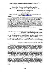
(a)
-W(110) Si
Intensity / a.u.
bias of −150 V was applied on the W coated substrates to induce the compressive stress in the W films. One set of W films prepared by RF magnetron sputtering were in-situ annealed inside the sputter chamber without breaking vacuum at 400◦ C for 1 h to obtain α-W phase. For a set of W films prepared by DC magnetron sputtering, a 30 nm Cr sticking layer was sputter-deposited prior to the W deposition.
-W(200)
-W(220)
-W(211)
-W(200) V IV III II
-W(210)
30
45
(b)
-W(400)
I
60
2
Intensity / a.u.
88
75
90
/ deg.
-W(110)
Si
-W(220)
Si
-W(200)
-W(211)
I
-W(200)
1
Si
-W(210) 30
40
2 50
60
2
-W(400)
II
70
80
90
/ deg.
Fig. 1 XRD patterns of W films: (a) XRD patterns of deposited and annealed W films prepared by RF magnetron sputtering: (I), 460 nm deposited W film; (II), 170 nm, (III), 300 nm, (IV), 460 nm and (V), 650 nm annealed W films, respectively, (b) XRD patterns of 410 nm W films prepared by DC magnetron sputtering: (I) α-W was obtained in W/30 nm Cr/Si system; (II) β-W in W directly deposited on Si substrates
3.1 Microstructures characterization Depending on the growth conditions, W thin films are usually made up of either the stable α phase (bcc lattice), the metastable β phase (A15 cubic lattice), or a mixture of both phases[11,16] . The occurrence of β phase has been observed previously in W films grown by sputtering and it could be stabilized by oxygen impurities in low concentration. Figure 1(a) shows the XRD patterns of the deposited and annealed W films prepared by RF magnetron sputtering on Si substrates. Obviously, the deposited W films are composed of β-W, while the annealed W films are totally composed of α-W and have the strong (110) texture. The XRD spectra for W/Cr bilayers prepared by DC magnetron sputtering are illustrated in Fig. 1(b). For comparison, the XRD spectra of the deposited W film without sticking layer is also appended into the Fig. 1(b). It is worth noting that the deposited W films with a 30 nm Cr sticking layer are composed of α-W, as shown in Fig. 1(b). It is evident that
there is a significant template effect that Cr seed layer has on the formation of α-W phase. A similar template effect was also observed in W/Mo bilayers[17] . There are no diffraction peaks of β-W in the overall diffraction range for W/Cr bilayer, which suggests that single-phase α-W film grows preferably on Cr layer due to template effect. As a matter of fact, once Cr atoms are stabilized, successive W atoms deposited on Cr will crystallize and grow with the same crystal structure as Cr (bcc) through a kinetic preference since the deposition temperature is 0.015 of the melting point of W and the diffusivity of W atoms is very low. Theoretically, the intrinsic reason is that interfacial energy can be effectively reduced by transforming the structure of two different kinds of layers into the same structure[17] . The minimization of interfacial and strain energy may be essential for template effect and size effect in W thin film. A cross-section morphology of the annealed 170 nm W film on Si substrates can be observed in
H.L. Sun et al.: J. Mater. Sci. Technol., 2010, 26(1), 87–92.
89
Fig. 2 Morphologies FE-SEM images of W films. (a)–(c), Cross-section images of 170 nm film, surface morphology of 170 nm and 460 nm annealed W films prepared by RF magnetron sputtering, respectively. (d) Schematically illustrates the compressive stress state of 460 nm deposited W films prepared by RF magnetron sputtering. (e) Surface morphology of 410 nm deposited W film prepared by DC magnetron sputtering. (f) Surface morphology of 410 nm deposited W film with a 30 nm Cr sticking layer
Fig. 2(a). A typical columnar feature of the grains is evident. Furthermore, the interface between the W thin film and the substrate is sharp and flat. The surface morphology of the annealed W films prepared by RF magnetron sputtering is shown in Fig. 2(b). It can be seen from Fig. 2(b) that the surface particles of the W films are very fine and uniform. Figure 2(c) implies that the in-plane average grain (column) diameter of the annealed 460 nm W film is in the range of 25–35 nm. Figure 2(d) schematically illustrates the compressive stress state of 460 nm deposited W films. Figure 2(e) shows the surface morphology of 410 nm deposited W film prepared by DC magnetron sputtering. It can be seen from Fig. 2(e) that the morphology of the particles on W films0 surface prepared
by DC magnetron sputtering is similar to that of annealed W films prepared by RF magnetron sputtering. However, the surface morphology of W films with a 30 nm Cr sticking layer differs from that of monolayer W films directly deposited on Si substrates, as shown in Fig. 2(f). The change on morphology is consistent with that of the crystal structure of W film with a 30 nm Cr sticking layer as indicated by XRD result. TEM was used to analyze the crystalline microstructures of the deposited 460 nm W films prepared by RF magnetron sputtering. The typical planar view of a dark-field TEM image of the W films is shown in Fig. 3(a). The grain size ranges from 20 nm to 40 nm, and the average grain size is about 25 nm. A selected area electron diffraction pattern is shown
90
H.L. Sun et al.: J. Mater. Sci. Technol., 2010, 26(1), 87–92.
Fig. 3 (a) Plane-view TEM image of the deposited 460 nm W thin film; (b) the corresponding electron diffraction pattern
curvature of film/Substrate system, and the residual stress of the W film on the Si substrate was calculated in terms of the Stoney equation. Figure 2(d) schematically illustrates the compressive stress state of deposited 460 nm W films on Si substrates prepared by RF magnetron sputtering. The residual stress of deposited 460 nm W film with a bias of −150 V is compressive with the value of about −925 MPa.
40
Grain size / nm
35 -W
30 25 20 15
3.2 Evaluation of mechanical property by nanoindentation 200
300
400
500
600
700
Film thickness / nm
Fig. 4 Grain sizes of the annealed W film as a function of film thickness
in Fig. 3(b), which indicates the films consist of pure W phase without any detectable other phases. The Voigt function and the extended Scherrer methods[18] were used to obtain the average in-plane grain size of the film. Prior to a calculation, the Kα1 was separated from the diffraction peak firstly, and then the half peak breadth and integration breadth of Kα1 were extracted to obtain grain size of films. Taking the α-W film as a sample, the calculated average grain sizes are plotted as a function of the film thicknesses in Fig. 4. It is clearly seen that the grain sizes of α-W increase monotonically with the film thickness. Among them, the grain size of the annealed 460 nm W film is about 32.5 nm. The average grain size of the deposited 460 nm W film is about 26.9 nm which is very close to the values (25 nm) obtained from the TEM photos. This indicates that the results obtained by calculation are in good agreement with the values observed from the TEM observation. It is well known that residual stress is very common in thin metal films, and even reaches several GPa. Previous studies have demonstrated that the residual stress in the film can affect the measured hardness value of thin films[19,20] . So, in this work, a BGS6341 optical profiler was used to measure the radius of
In order to fully investigate the mechanical behaviors of W films, both the hardness and modulus of the deposited and annealed W films prepared by RF magnetron sputtering were characterized by nanoindentation. Firstly, taking the annealed 460 nm W films as a sample, the load-displacement curves were analyzed and certain information from these curves is ascertained. Following this, the hardness and modulus were obtained via the Oliver-Pharr and Doerner-Nix methods, respectively. Figure 5 shows the load-displacement curves of the annealed 460 nm W film. The load-displacement behaviors are typical for a hard metal and it is evident that there are very high amounts of elastic recovery in comparison with Cu and Al, as shown in the unloading curve. It is clearly seen in Fig. 5 that all the load-displacement curves are in good agreement with each other except one of them deviating from others greatly which is due to film fracture during loading (indicated by a filled arrow). The kick-back in unloading is caused by the undensification of silicon[21] . The hardness and modulus of the deposited and annealed 460 nm W films are plotted as a function of indentation depth in Fig. 6. It is clearly seen that the plateaus which characterize the true mechanical property exist on the hardness curves but not for the modulus curves. This implied that, compared to hardness, the elastic modulus of thin films is more strongly affected by the elastically inhomogeneous substrate
91
H.L. Sun et al.: J. Mater. Sci. Technol., 2010, 26(1), 87–92. 150 Experimental data of deposited W film Experimental data of annealed W film
0.005
120
Fitted line of deposited W film Fitted line of deposited W film
y = A *exp(-x/t ) + y R = 0.98515 y = 0.00239 ± 0.00008 A = 0.00313 ± 0.00011 t = 5.18416 ± 0.49282 Equation: y = A *exp(-x/t ) + y R = 0.99156 y =0.00248 ± 0.00004 A =0.00331 ± 0.00009 t =3.13098 ± 0.18439 Equation:
deposited
1
1
0
0
E GPa
-1
90 60
1
0.004
1
annealed
1
1
0
2
0
1 /
Load / mN
2
1
0.003
1
30 0
0
200
400
600
800
0.002 0
Hardness / GPa
Modulus/ GPa
Fig. 5 Load vs. indentation depth of the annealed 460 nm W films on Si substrates
400 300
Hardness of
-W
Hardness of
-W
10
15
Modulus of
-W
Modulus of
-W
Fig. 7 Reciprocal of the modulus vs. t/h for the deposited and annealed 460 nm W films (solid line is the fitted line using Eq. (1))
³ 1 1 1 ¢ −α(t/h) 1 = + − e E Ef Esb Ef
20 10 0
100
200
300
400
20
tic properties of the films from those of the substrates according to the measured nanoindentation data[15,24,25] . One of the successful models is Doerner and Nix model. In the model of Doerner and Nix, the empirical relationship among E, Ef , and Esb is
200
0
5
t/h
Indentation depth / nm
500
Film thickness / nm
Fig. 6 Hardness and modulus of the deposited and annealed 460 nm W films as a function of indentation depth
when the film is very thin. At small indentation depths, the hardness increases with increasing depth due to strain gradient effect[22] . At deeper indentations (about in the range of 80–160 nm), the plateaus which characterize the intrinsic hardness of thin film[23] appear in the curves and the hardness reaches nearly constant. Then the hardness starts to decrease with increasing indentation depth, which are attributed to the softening effect caused by the soft substrates. In the present work, we take the average hardness in the range of the plateaus of hardnessindentation depth curves as the intrinsic hardness of W films[23] . With 10 indentations, the average hardness is 24.5±1.6 GPa and 21.3±1.1 GPa for the deposited and annealed 460 nm W films, respectively, which are slightly higher than that of W films (17.9 GPa) reported[6] . Furthermore, the hardness of W films are significantly higher than other metal thin films, for instances, 11.6 GPa for Ta[6] and 11.8 GPa for Mo[7] , which is consistent with the fact that bulk W is evidently harder than other pure bulk pure metals. The hardness of the 460 nm W films is slightly higher than that of other W films with different thickness prepared in the present work. Many models were proposed to separate the elas-
(1)
where α is a constant, t is the film thickness, h is the penetration depth, f and sb represent the film and the substrate, respectively. In the present work, this model is used to analyze the nanoindentation data and consequently to obtain the modulus of the W films. Figure 7 is a plot of 1/E vs t/h for the 460 nm deposited and annealed W films. The solid line is the fitted results by using a least-squares method according to Eq. (1). Their modulus obtained from the fitting data are 403 and 418 GPa for the deposited and annealed 460 nm W films, respectively, which are very close to the Young0 s modulus reported for conventional bulk W (410 GPa). The modulus of deposited W film is slightly higher than that of annealed W films, which may be ascribed to its high atom density in crystal lattice. 3.3 Discussion The nanoindentation hardness of sputtering deposited thin films is related to many factors such as experimental parameters, impurities, residual stress and tip geometry, grain size and dislocation density of the film. In this work, the huge hardness found in deposited and annealed W films on Si compared with the hardness of bulk W can be ascribed to a larger compressive stress (−925 MPa) and smaller grain size (about 32.5 nm). Previous studies have indicated that a larger compressive stress can lead to a higher hardness[19,20] The origin of the larger compressive stress is attributed to the bombardment of energetic particles because of a small target-substrate distance (only 70 mm) and application of a bias of −150 V.
92
H.L. Sun et al.: J. Mater. Sci. Technol., 2010, 26(1), 87–92.
In the mechanism of dislocation piling up, the grain size dependent hardness of traditional polycrystalline metals is usually described by the wellknown Hall-Petch relation, H=H0 +Kd−1/2 where H0 and K are material dependent constants. Therefore, with decreasing grain size, the hardness of nanocrystalline material is usually much higher than that of bulk coarse-grained materials. In addition, it is demonstrated[26] that grain boundaries in bcc-metals are more effective in blocking dislocation motion. The volume fraction of grain boundary and triple line junction increases rapidly with decreasing grain size, which suggests that at smaller grain size the effect of grain boundary and triple line junction on the deformation becomes important. According to the conventional theory of dislocation pile-up, the critical grain size dc for a maximum hardness or strength can be expressed as[27] dc = G · b/π · (1 − ν) · σapp
(2)
where G is the shear modulus, b is the Burgers vector, ν is the Poisson0 s ratio, and σapp is the external applied stress. Inserting the yield strength of the pure coarse-grained W, about 687 MPa, as σapp , into Eq. (2), we get the critical grain size for the maximum hardness at about 29.1 nm. It is worth noting that the critical grain size is very close to the average grain size of the W thin films. 4. Conclusion W thin films were prepared by RF and DC magnetron sputtering onto Si (100) substrates. The results show that a thin Cr sticking layer can induce structure changes of deposited W film from β-W to α-W structure. In addition, remarkable hardness enhancement both for the deposited and annealed W films was observed, compared with that of bulk coarse-grained W, although their nanoindentation modulus is very close to that of corresponding bulk W. The super hardness found in deposited and annealed W films can be ascribed to smaller grain size and a larger compressive stress and is anticipated to be of great scientific and technological interest. Above results provides a strategy to fabricate α-W films.
Acknowledgements This work was supported by the National Basic Research Program of China (No. 2004CB619302) and the National Natural Science Foundation of China (No. 50871083, 50771078 and 50771069).
REFERENCES [1 ] A.H. Chokshi, A. Rosen, J. Karch and H. Gleiter: Scripta Mater., 1989, 23, 1679. [2 ] C.A. Schuh, T.G. Nieh and H. Iwasaki: Acta Mater., 2003, 51(2), 431. [3 ] J. Schiotz and K.W. Jacobsen: Science, 2003, 301, 1357. [4 ] H. Gleiter: Acta Mater., 2000, 48(1), 1. [5 ] K.S. Kumar, H.V. Swygenhoven and S. Suresh: Acta Mater., 2003, 51(19), 5743. [6 ] M. Zhang, B. Yang, J. Chu and T.G. Nieh: Scripta Mater., 2006, 54(7), 1227. [7 ] K.B. Yoder, A.A. Elmustafa, J.C. Lin, R.A. Hoffman and D.S. Stone: J. Phys D: Appl. Phys., 2003, 36, 884. [8 ] M. Itoh, M. Hori and S. Nadahara: J. Vac. Sci. Technol. B, 1991, 9(1), 149. [9 ] M.S. Aouadi, R.R. Parsons, P.C. Wong and K.A.R. Mitchell: J. Vac. Sci. Tehnol. A, 1992, 10(2), 273. [10] K.Y. Ahn: Thin Solid Films, 1987, 153(1-3), 469. [11] S.M. Rossnagel, I.C. Noyan and J.C. Cabral: J. Vac. Sci. Technol. B, 2002, 20(5), 2047. [12] V.G. Glebovsky, V.Y. Yaschak, V.V. Baranov and E.L. Sackovich: Thin Solid Films, 1995, 257(1), 1. [13] S. Eroglu, H. Ekren and T. Baykara: Scripta Mater., 1997, 38(1), 131. [14] W.C. Oliver and G.M. Pharr: J. Mater. Res., 1992, 7, 1564. [15] M.F. Doerner and W.D. Nix: J. Mater. Res., 1986, 1, 601. [16] M.J. O0 Keefea and J.T. Grant: J. Appl. Phys., 1996, 79(12), 9134. [17] M.X. Liu, Y.L. Huang, F. Ma and K.W. Xu: Mater. Sci. Eng. B, 2007, 139, 99. [18] B.F. S´ anchez and A.L. Ortiz: Acta Mater., 2006, 54(1), 1. [19] Y.X. Yao and Y. Zhu: Key Eng. Mater., 2004, 258259, 180. [20] G. Abadias, S. Dub and R. Shmegera: Surf. Coat. Technol., 2006, 200(22-23), 6538. [21] G.M. Pharr, W.C. Oliver and D.S. Harding: J. Mater. Res., 1991, 6, 1129. [22] W.D. Nix and H.J. Gao: J. Mech. Phys. Solids., 1998, 46(3), 441. [23] R. Saha and W.D. Nix.: Acta Mater., 2002, 50(1), 23. [24] H. Gao, C.H. Chiu and J. Lee: Int. J. Solids Struct., 1992, 29(20), 2471. [25] J. Li and W. Chou: Int. J. Solids Struct., 1997, 34(3536), 4463. [26] H.S. Kim, Y. Estrin and M.B. Bush: Acta Mater., 2000, 48, 493. [27] T.G. Nieh and J. Wadsworth: Scripta Metall. Mater., 1991, 25, 955.