Apr 7, 2015 - ... discriminate. Preprint submitted to ARC 2015. The final publication is available at link.springer.com. arXiv:1504.01718v1 [cs.AR] 7 Apr 2015 ...
Modular Acquisition and Stimulation System for Timestamp-driven Neuroscience Experiments
arXiv:1504.01718v1 [cs.AR] 7 Apr 2015
Paulo Matias, Rafael T. Guariento, Lirio O. B. de Almeida, and Jan F. W. Slaets S˜ ao Carlos Institute of Physics University of S˜ ao Paulo S˜ ao Carlos, SP, Brazil {matias,guariento,lirio,jan}@ifsc.usp.br
Abstract. Dedicated systems are fundamental for neuroscience experimental protocols that require timing determinism and synchronous stimuli generation. We developed a data acquisition and stimuli generator system for neuroscience research, optimized for recording timestamps from up to 6 spiking neurons and entirely specified in a high-level Hardware Description Language (HDL). Despite the logic complexity penalty of synthesizing from such a language, it was possible to implement our design in a low-cost small reconfigurable device. Under a modular framework, we explored two different memory arbitration schemes for our system, evaluating both their logic element usage and resilience to input activity bursts. One of them was designed with a decoupled and latency insensitive approach, allowing for easier code reuse, while the other adopted a centralized scheme, constructed specifically for our application. The usage of a high-level HDL allowed straightforward and stepwise code modifications to transform one architecture into the other. The achieved modularity is very useful for rapidly prototyping novel electronic instrumentation systems tailored to scientific research. Keywords: Spiking Neurons, Data Acquisition, Precise Timing, Resource Arbitration, Latency Insensitive, Modular Design.
1
Introduction
Neurons usually behave by emitting stereotyped pulses of electric depolarization through their membranes, creating temporally localized spikes. It is a common belief that spiking neurons follow an all-or-none principle, similar to the processing of digital signals, by encoding information only through spike timing [1]. Although each individual cell always produces the same waveform, the most widespread experimental approach employs Analog to Digital Converters (ADCs) integrated on commercial acquisition systems to capture complete waveforms. This procedure is required when the researcher desires to analyze a large population of neurons recording only from a few electrodes, applying then a neuron classification technique known as spike sorting to discriminate Preprint submitted to ARC 2015. The final publication is available at link.springer.com.
individual waveforms [2]. However, because of the lack of readily available specialized acquisition hardware, many works adopt the same recording technique even though they only need to identify the occurrence of spikes from one neuron per electrode [3,4,5,6]. The resulting data files are large and spikes need to be detected by software, demanding a considerable amount of time. In this paper we present the design of a low-cost alternative hardware solution based on a dedicated Complex Programmable Logic Device (CPLD). We have chosen CPLDs instead of Field Programmable Gate Arrays (FPGAs) to demonstrate the flexibility of our approach, as CPLDs are usually limited to a small number of logic gates, and lack common FPGA features such as Block RAMs and Phase Locked Loops (PLLs). We implemented the logic circuits on the CPLD adopting a modular design, which aims to facilitate future refinement and customization for specific applications. The complete source code implemented in the Bluespec SystemVerilog (BSV) [7] language is available at [8]. BSV designs targeted at small reconfigurable devices, such as ours, are rare in literature, since many works show that BSV usually produces a higher logic element (LE) count than Register-Transfer Level (RTL) languages [9,10,11]. However, some research [12] argues that microarchitectural choices have greater impact on the LE usage than the specification’s abstraction level, although there is a lack of studies in glue logic sized architectures with significant modularity and complexity. This paper showcases such a system, and also explores the impact of latency insensitive module decoupling [13], by comparing two distinct implementations of a resource arbitration scheme. Similar work evaluating synthesis results exists [14], but we also test the consequences on system resilience to extreme conditions, many times above our application requirements. The acquisition input is provided to our digital logic by an analog front-end system which generates an asynchronous TTL-compatible signal pulse at the occurrence of each valid spike. Our entire circuit was designed to be compatible and easily inserted into a previous experimental setup [15] devised for studying neural codification in Chrysomya megacephala’s visual system, but it is sufficiently generic to be suitable for a wide range of neuroscience experiments.
Main contributions of this work: – Develops a portable, low-cost and precise data acquisition system for neuroscience and neuroethology experiments. – Applies the seldom used concept of recording digital events (instead of ADCconverted data) to increase the precision of neural spike timing. – Employs the BSV language in a small and resource constrained system. – Showcases architecture refactoring from a decoupled to a centralized scheme.
Paper organization: The next section describes the basic specifications of our design and its overall architecture. Section 3 discusses the system implementation, focusing on points common both to dynamic and static arbiter versions. Sections 3.1 and 3.2 delve into specific aspects of each one of the implementa2
tions. Section 4 presents synthesis, experimental and simulation results. Finally, we conclude in Section 5.
2
Overall system architecture
Our system offers 6 TTL-level pulse timestamp acquisition inputs, 4 analog 16-bit resolution outputs for stimuli generation and a Join Test Action Group (JTAG) host computer interface. It is composed by a MAX II Micro Kit (EPM2210F324C3 CPLD), a 74HC4050 buffer for input overvoltage protection, a MAX5134 Digital-to-Analog Converter (DAC) and a IDT71256 20ns 32K×8bit SRAM. We have divided the project in following functional subunits: Synchronizer: Receives asynchronous input pulses and registers 32-bit timestamps from a hardware counter, each one paired to a flag indicating which input channels fired since last counted. In most neural systems, 1 µs is believed to be enough resolution for studying fine details of information coding [16]. FIFO SRAM: Provides an interface for using the external SRAM memory as a pair of First-In First-Out (FIFO) queues of 16 KiB each. One of them buffers data acquired from inputs, and the other buffers stimuli received from a computer. Our FIFO modules are compatible with the BSV standard library. JTAG interface: Provides communication with a host computer. We have wrapped Altera JTAG-UART libraries into a ready-to-use BSV module. By using this protocol, the same communication module is portable to any CPLD or FPGA manufactured by the same vendor. As programmable devices are configured via JTAG, the bus is readily available through USB adapters embedded in almost every evaluation board. However, this approach introduces a significant protocol overhead by encapsulating UART emulation inside JTAG-USB, limiting the data rate to about 1 Mbit/s. Also, client software needs to explicitly poll the device, because the interface is not interrupt nor event driven. This results in software determinism becoming a bottleneck depending on hardware buffer size and desired data rate. Nevertheless, these limitations do not impair this particular application.
3
BSV module architecture
Bluespec SystemVerilog is a strongly typed high-level hardware description language (HDL) with functional paradigm features. A BSV design is organized in modules and rules. Modules provide interfaces, composed by a set of methods which can be used to access or modify their internal state. State changes (sideeffects) are clearly separated from read-only operations by the means of a monad [17] called Action, thus any expression which modifies state has an action type. Modules can be statically elaborated several times, allowing to represent complex circuit structures. Rules are entities which describe the connections between modules and ultimately define hardware dynamics. They are formed by a set of actions and a boolean predicate, which defines an explicit condition needed to allow execution of the actions (rule firing). During a single clock cycle, a rule is 3
guaranteed to entirely complete its execution or not to fire at all, property known as transaction atomicity. Rule firing can also be affected by implicit conditions, which can be attributed to any BSV expression. The BSV compiler propagates an implicit condition back to the predicate of the rule which actually executes the action or queries the value of the corresponding expression. Implicit conditions are usually attributed to method boundaries, serving as an effective way to specify module contracts. When synthesizing, the compiler defines an execution order for rules, allowing a hardware scheduler to be generated according to the Term Rewriting Systems (TRS) formalism [18].
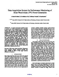
SER
Synchronizer acqIn inputs
inSyncs
syncedIn
wires mkAsyncPulseSync wiresmkAsyncPulseSync
Bits#(NumInputs)
timestamp 32 bits +1
dacLoad
timestampUpdate blendChannelFlags
funnel in
channelFlags 0 1 0 0 0 1 1 0
FIFO SRAM
sram mkSRAMSplit
SRAM
wires
DAC dac DAC
wires
DES load
mkDAC
req
dacHandleReq
uartOutFifo cli
srvB srvA
unfunnel
mkFunnel
uartInFifo cli
fifo
mkSRAMFIFO
mkUnfunnel out in fifo
out
JTAG
uart tx mkAlteraJtagUart rx
uartHandleCmd
Fig. 1. Block diagram of the BSV modules and rules. The gray shaded areas represent internal logic, while white structures depict I/O interfaces. Modules are portrayed as quadrilaterals. The names inside them are module names, and those outside are instance names. Small rectangles on their side are interfaces. Ellipses designate rules. Those which only perform connections are omitted and represented directly by arrows.
Figure 1 illustrates our main module. The fundamental difference between arbitration approaches resides on SRAMFIFO internals and on how communication with the SRAM occurs. In the dynamic approach this is done by a client-server interface mediated by FIFOs, whereas in the static one an extra central module exists which assigns a specific operation to the SRAMFIFOs on each cycle. Acquisition data flow: Asynchronous pulses arriving from acquisition inputs are synchronized to the system clock by the AsyncPulseSync modules, resulting in the syncedIn signal. The blendChannelFlags rule accumulates one bit for each input channel in the channelFlags register, if a pulse occurred on syncedIn since the last collected timestamp. The timestampUpdate rule atomically increments the timestamp register, sends the channelFlags value and the current timestamp to the funnel, and resets channelFlags to zero. The funnel emits one byte of its input per cycle to the uartOutFifo. Finally, data coming 4
from dataOutFifo can be read in the host computer after being collected by the JTAG-UART transmitting (tx) interface. Stimulus generation data flow: Begins at the JTAG-UART receiving (rx) interface. The uartHandleCmd rule identifies if the byte received from the computer represents a start command or a DAC conversion request. A start command sets a boolean register (omitted from the figure) which unblocks the predicate of dacLoad, timestampUpdate and blendChannelFlags rules. A DAC conversion request sends the current byte and the next two bytes to uartInFifo. After coming out of the FIFO, the bytes feed the unfunnel block, merging three bytes together. The dacHandleReq controls the request flow to the DAC module. The dacLoad rule fires when the first input channel receives a pulse, unblocking the dacHandleReq rule and causing a synchronous update on all DAC outputs. This input channel is used to synchronize analog outputs to the desired stimuli clock, e.g. the display controller in a visual stimulation system. BSV has an implicit condition mechanism which eases the specification of a provably correct system. We only needed to add error handling to four places of our design. The first one is related to tx path FIFO overflow and is put in the timestampUpdate rule, ensuring that the timestamp is always incremented at each update period. The second check is accomplished in the dacLoad rule, and verifies if a FIFO underrun has occurred in the rx path, by certifying that the DAC is ready to receive a new command and that all DAC registers were filled since the last load. The final two are not directly related to system functional correctness, but to good debugging practices. The third one checks if bytes received from JTAG-UART correspond to valid commands. The last one verifies if DAC requests are still valid after leaving uartInFifo, aiming to detect any occurrences of data corruption during communication with the SRAM chip. When any of these error condition occurs, we alert the user by blinking LEDs until the system is reset. Next, we describe characteristics of the common system sub-modules. SER/DES: Serializer and deserializer modules are implemented using shift registers. Our design is generic and type parametrized, making it reusable with any input or output data types. A code excerpt illustrating these concepts is shown in Figure 2. DAC: In order to rapidly prototype the control of a Serial Peripheral Interface (SPI) and DAC linearity calibration procedures, we employed a standard BSV library called StmtFSM, which consists of a Domain Specific Language (DSL) for specifying Finite State Machines (FSMs). The FSMs could be easily composed and exposed in the form of a simple external module interface. DAC register update requests supported by the MAX5134 DAC contain three bytes, one specifying the target channels and two bytes of data. Part of the FSM implementation is illustrated in Figure 3. SRAMFIFO: This module is also type parametrized. It exposes a fifo subinterface mimicking BSV standard library’s mkLFIFO, and a cli subinterface which can be connected to a SRAM or SRAMSplit server interface. Usage of Ephemeral History Registers (EHRs) [19] greatly simplified the design in or5
// Defines an interface for generic types a and b interface Funnel#(type a, type b); // ... endinterface function Funnel#(a,b) toFunnel(FIFOF#(a) infifo, FIFOF#(b) outfifo); return (interface Funnel; method Bool notFull = infifo.notFull; // ... endinterface); endfunction module mkFunnel(Funnel#(a,b)) // ... rule firstCycle(stage == 0); // Shifts the input value from infifo shiftReg