15.1
A Multi-port Current Source Model for Multiple-Input Switching Effects in CMOS Library Cells Chirayu Amin, Chandramouli Kashyap, Noel Menezes, Kip Killpack, and Eli Chiprout
[email protected] Strategic CAD Labs, Intel Corporation, Hillsboro, OR 97124
ABSTRACT The problem of multiple-input switching (MIS) has been mostly ignored by the timing CAD community. Not modeling MIS for timing can result in as much as 100% error in stage delay and slew calculation. The impact is especially severe on stages immediately after a bank of flops, where the inputs have a high probability of arriving simultaneously. Other problems such as modeling of interconnect loads, complex (nonlinear/non-monotonic) input waveforms, power-droop impact on cell delay, nonlinear input capacitances, delay variations due to cross-capacitance, etc. are also known sources of error. In this paper, we introduce the multi-port current source model (MCSM). MCSM can efficiently handle an arbitrary number of simultaneously switching inputs, including single-input switching (SIS). Moreover, MCSM is comprehensive in that other modeling problems associated with delay and noise computation are elegantly covered. We demonstrate the applicability of MCSM on a large 65 nm industrial test-case. For cells experiencing MIS, the model yields delay and slew-rate errors within ±5% for 88.3% and 93.0% of the cases, respectively. We also present data that show that MCSM is an effective receiver model which captures active loading effects without incurring significant additional error. MCSM makes combined cell-level timing, noise, and power analysis a possibility.
slew
Vcc
MIS Vss
cross-cap nonlinear load interconnect
delay
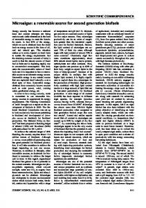
other sources: process/env. variations nonlinear waveforms Figure 1. Delay variations in modern technologies [7] models are traditional in that the characterization is still in terms of the input slope (or slew-rate) and output capacitive load. From this perspective, these models address only a few of the challenges outlined above. Moreover, these models still require a Ceff procedure [2] to map the interconnect load to one linear capacitance value to calculate gate delays. The CSM proposed by Croix and Wong [11] is a more natural model in that it is independent of the input waveform and output load. The model is essentially a ViVo-based (input voltage, output voltage), DC-transfer-derived current source with transient effects modeled by a linear capacitance at the output. A linear capacitance to model the cell active input load is assumed. The authors of [11] also indicate that a load-dependent time shift may be required to enhance the accuracy of their model. This load-dependent time shift takes away some of the inherent elegance of their model. Keller, et al. [12] demonstrated that the Croix CSMs work well for modeling cross-capacitance (noise-on-timing) effects while hinting that a nonlinear capacitor may be required at the output.
Categories & Subject Descriptors: B.7.2 Design Aids – Simulation, Verification, B.8.2 Performance Analysis and Design Aids General Terms: Performance, Verification, Design Keywords: multiple input switching, current source model, timing analysis, cell library characterization, cell model, MCSM
Li and Acar [13] following the suggestion of [12] introduce a nonlinear output capacitance model. Their paper describes a characterization technique for deriving the voltage dependent output capacitance. Furthermore, they also introduce a 2-RC ladder network at the input to model the nonlinear nature of cell loads. Since the RC delay of the ladder network introduces an inherent time shift from the input waveform, this model can also be applied to multi-stage cells. Unfortunately, the experimental data in [13] is limited to only a few cells.
1. INTRODUCTION Figure 1 illustrates the challenges that cell delay models [1] currently face. In modern CMOS technologies, in addition to modeling resistive interconnect effects [2], it is important to model a) complex input waveforms [3], b) power-droop, c) delay variation due to cross-capacitance [4], d) MIS [5], e) the nonlinear input capacitance [7], and f) process variations [6]. Current source-based models (CSMs) have recently received increased attention with major EDA vendors announcing support for these models [8][9]. The model proposed by Tutuianu et al. [10] is also similar to [8][9]. These vendor CSMs claim to primarily address accuracy concerns associated with the dominant delay model [2]. Essentially, the vendor CSMs derive their enhanced accuracy through characterization at more time points (10%, 30%, 50%, 70%, 90%, etc.) compared to the model in [2]. However, these
The problem of modeling MIS accurately has largely been ignored by the timing CAD community. Some research has been presented in [14]-[16] but unfortunately the underlying models are ad-hoc approaches to the MIS problem and require significant effort in characterization. Moreover, the analysis is not accurate enough. Also the models proposed in [14]-[16] are prohibitively expensive and/or ineffective if a gate has more than two inputs. Leveraging previous work, we introduce MCSM, the multiport generalization of CSMs. MCSM can adequately model the MIS effect for combinational cells. MCSM works by characterizing the charge, in addition to the current, injected at each of the pin inputs and outputs in a voltage dependent manner. Our charge interpretation, as opposed to a capacitance view, also provides insight into the necessity of modeling the nonlinear capacitances at each cell input. Moreover, other models do not naturally capture
Permission to make digital or hard copies of all or part of this work for personal or classroom use is granted without fee provided that copies are not made or distributed for profit or commercial advantage and that copies bear this notice and the full citation on the first page. To copy otherwise, or republish, to post on servers or to redistribute to lists, requires prior specific permission and/or a fee. DAC 2006, July 24–28, 2006, San Francisco, California, USA. Copyright 2006 ACM 1-59593-381-6/06/0007…$5.00.
247
effects such as complex input waveforms, interconnect effects, power-droop, cross-capacitance, nonlinear input capacitance, etc. Our model, MCSM, is comprehensive in that most of these can be elegantly covered without tweaking the model, thus addressing one of the major problems with STA flows today in that a different model is used for each phenomenon.
p1
p2 p3 pn-2
a b out
QC,pn-1
(MCSM) ipn-2
ipn iR,pn-2
iR,pn
pn
QC,pn
where fi and gi are precharacterized functions (stored as tables or equations) of port voltages vpi. For example, the MCSM for a twoinput nand gate will consist of three ports – one for each input and output – with a precharacterized iR and QC at each port. MCSMs can be thought of as a higher-level version of transistor models. A transistor can be viewed as a nonlinear conductance under steady state conditions. However, modeling the transient behavior of a transistor requires complicated nonlinear capacitances. As described in [17], it is more convenient to model the transient behavior with charges associated with the terminals of the transistor. In general, these charges are complex, nonlinear, time-varying functions but are approximated as nonlinear, timeindependent functions of the terminal voltages. For example, the drain charge QD can be expressed as QD = f(vD,vG,vS,vB) where vD, vG, vS, and vB, are the terminal pin voltages. Note that for a transistor both the nonlinear conductance and the nonlinear charges are characterized as functions of pin voltages and are not time-varying. Extending this analogy to cells, for a post-extraction cell consisting of multiple transistors, diodes, resistors and capacitors, our model assumes that the pin voltages determine the nonlinear conductance iR and the nonlinear charge QC at each of the pins.
SIS
MIS
Figure 2. MIS has a major impact on timing As we will show in the results section, not modeling MIS can result in as much as 100% error in delay and slew per stage (see Figure 10). The impact is especially severe on stages right after a bank of flops, where the inputs have a high probability of arriving simultaneously. Thus, properly modeling MIS is necessary for accurate timing analysis. In the next section, we describe our cell model for capturing MIS.
For cells with multiple channel connected components (CCCs), we propose generating MCSMs for each of the CCCs. During analysis, we propose that MCSMs for all the CCCs in a cell be combined and then analyzed. The behavior of the model for domino and sequential cells remains untested but we expect the model to work as long as these cells are broken into multiple CCCs. Unlike [13], which does not attempt to address MIS, our model captures the concurrent switching behavior at all inputs since the iR and QC at each port are functions of the voltages at all ports. Furthermore, the authors of [13] proposed to model the input of the gate by a two-pole RC circuit which may not adequately capture the nonlinearity of the input capacitance, unlike our model. In our experience, capturing the nonlinear nature of cell input loading is important (see [7] for more details). In our model, the Miller capacitance at the input nodes of regular CMOS cells is captured by the QC since in addition to the voltage at the input ports of interest, it also depends on the voltages at the other ports in the cell including the output port.
3. A MULTI-PORT CURRENT SOURCE MODEL (MCSM) Our multi-port current source model (MCSM) consists of a nonlinear resistor in parallel with a nonlinear capacitor at each input and output pin (or port) of the cell. This follows [13], which applies a similar model to the output pin only. We represent the resistor by a voltage-controlled current source (iR) and the capacitor by a voltage-controlled charge (QC) as shown in Figure 3. Since each port in a nonlinear cell could behave differently, it is reasonable to expect that the voltage-dependent value of iR and QC at each port is different. More formally, at each port pi (i = 1, 2, …, n), the voltagecontrolled current source and charge is given by : iR , pi = f i (v p1 , v p 2 , K, v pn ) (1)
QC , pi = g i (v p1 , v p 2 ,K , v pn )
iR,pn-1
Figure 3. Multi-port Current Source Model
Figure 2 illustrates the MIS effect on a two-input nand gate. If inputs a and b arrive simultaneously, then the gate delay is significantly different than in the situation when one of the inputs has been stable for a long time. When a and b rise simultaneously, the gate delay and output slew increases. Most STA tools apply SIS gate delay/slew models even if the timing windows for the input signal would predict an MIS event. This can result in a significant under-estimation of gate delay/slew and makes MAX delay analysis optimistic. Similarly, if a and b fall simultaneously, the delay/slew can be significantly over-estimated and this makes MIN delay analysis optimistic. The problem is exacerbated for cells with more than two inputs switching simultaneously.
out
iR,p1
pn-1
MULTI-PORT CSM
QC,pn-2
2. IMPACT OF MIS ON TIMING
a b
ipn-1 QC,p1
We begin by giving an overview of the MIS problem and its impact on static timing analysis in Section 2. We then describe our multi-port CSM in Section 3. The characterization procedure for our model as well as the model’s usage in a timing analyzer is detailed in Section 4. Comprehensive accuracy comparisons for SIS and MIS assumptions are demonstrated on a 65 nm static CMOS library and test-case in Section 5, along with receiver modeling data. Conclusions and suggestions for future work are presented in Section 6.
a b out
ip1
(2) 248
4. MCSM CHARACTERIZATION AND USAGE
Figure 4a shows QC for output o of a two-input nand gate as a function of the voltage at input b (with input a held high). It is clear from this figure that QC can be quite nonlinear and a linear approximation, which implies a constant capacitor, will not suffice. This is demonstrated from the large slew error we see in Figure 4b using an optimized linear capacitance. The problem is worse for cells with more than two inputs.
0
0
(5)
Even though library characterization is a one time effort for a stable process technology, it is nevertheless desirable to get an idea of the time for the proposed methodology. For m voltage sample points in the range of [Vss-Δv,Vcc+Δv], mn dc simulations and mn transient simulations are required for an n-port cell. Since dc simulation is relatively inexpensive and the maximum value of n is limited to 5-6 in a typical cell library, this is still practical. Our experiments indicate that m=15 is practical from both accuracy and characterization run-time perspectives. On the other hand, transient simulations can become expensive for n ≥ 4. We used m = 15 for iR characterization and m = 7 for QC characterization for these cells. The slight loss in accuracy of QC can be tolerated because the nonlinearity of QC, which represents internal cell parasitics, is less than that of the drive current iR. Further, in many practical situations the load driven by the gate dominates the internal parasitics so the error introduced due to a coarser sampling of the QC space is within acceptable limits. A 4-input cell with extracted parasitics can be fully characterized in five minutes on a 3GHz machine. We are investigating intelligent sampling techniques to speed up characterization without compromising accuracy.
Input Model SPICE
vout=Vss 0
0 T
4.3 Characterization complexity
V/Vcc 1.0
Vcc
0 T
The left hand side of (5) represents QC,pi, which is the desired charge at port pi for that particular combination of port voltages. QC,pi can be calculated from (5) since the first term on the right hand side is obtained from the transient simulation. The second term is simply the dc (or steady stage) current, iR,pi, multiplied by T which is characterized as described in Section 4.1. In this regard, our approach is similar to [13], except that we measure and store QC at each port as a function of all the port voltages. It is easy to observe that the same transient simulation can be used to calculate QC for all the ports corresponding to that particular combination of voltages. We store the resulting data in a lookup table but an empirical equation fitted to the data can also be used to reduce model storage.
4.2 Charge (QC) characterization
vb
0
Here it is assumed that the initial charge Q0 is zero at t = 0 when voltages are zero at all the ports. (A non-zero charge at t = 0 is simply an offset that does not affect the instantaneous capacitance, which is given by the derivative that gets used in the MCSM based simulation.) We select the final value T to be large enough to ensure that all transients die out.
This aspect of the characterization is relatively simple and similar to previous CSMs. The dc current source for each port (f in equation (1)), is obtained by attaching a dc voltage source at each port and sweeping the voltages in the range of [Vss-Δv, Vcc+Δv] at each port. We choose Δv to be sufficiently large so as to accommodate below/above rail voltage spikes. We then measure the input current at each port pi to obtain fi. Hence, for a particular voltage level at a port a dc simulation is carried out for all intermediate voltage levels at all the other ports. We apply equal voltage increments at all ports during the dc sweep in our implementation. Consequently, at the end of this process, we have the dc currents at each port stored in ndimensional tables (where n is the number of ports). The computational complexity of the entire characterization process is discussed later in section 4.3.
0
T
QC , pi = ∫ i pi (t ) dt − ∫ f i (v p1 (t ),K, v pn (t ))dt (Q Q0 = 0)
4.1 Current source (iR) characterization
QC
T
∫ iC , pi (t )dt = ∫ i pi (t )dt − ∫ iR, pi (t )dt + Q0
Having described the basic model, we next describe the MCSM characterization process. Then we describe MCSM usage in a timer and highlight the advantages of MCSM.
vout=Vcc
T
2 3 1 Time [normalized to FO4 delay]
(b) >10% slew error due to linear approximation of QC Figure 4. QC,output for a two-input nand in a 65 nm static CMOS technology with input a held HIGH
(a) Nonlinearity of QC,output
If QC were indeed linear with respect to port voltages, then ∂QC/∂v (= C) is constant, and the linear capacitance models presented in [10]-[12] apply. Since this is not the case for our technology, we apply a different characterization methodology for obtaining QC.
4.4 Model usage during timing analysis Typically during timing analysis, we are interested in calculating the delay of a driver loaded by several fanout receivers with interconnections represented by RC parasitics. The driver is driven by waveforms obtained from the previous stage. Our model is general enough to be used with any transient simulation strategy: explicit or implicit. We model the combined driver-interconnectreceivers as a single circuit, called a stage, with MCSM models used for the driver and receivers. We then apply appropriate input waveforms to this setup. The resultant circuit representation is analyzed in a single simulation.
As would be expected, we characterize QC as a function of the port voltages. To measure QC for a specific combination of port voltages (V1, V2, …, Vn), we apply a step signal at each ports pi with value: v pi (t ) = Vi ⋅ u (t ) (3) where pi is the ith port and u(t) is the unit step function. Hence, we require a transient simulation for each combination of input voltages (each entry in the QC lookup table). For obvious reasons, we apply a fast ramp instead of a step in our circuit simulator. Referring to Figure 3 and applying Kirchoff’s current law at port pi, we have:
We have implemented the model in a prototype stage simulator using constant time steps. During circuit simulation, the port current ipi for the MCSM is given by:
iC , pi = i pi − iR , pi (4) where ipi, iC,pi, and iR,pi are the currents through the port, the nonlinear capacitor, and the nonlinear resistor, respectively. Integrating the hypothetical current through the nonlinear capacitor – integrating (4) – yields a technique for calculating a charge approximation: 249
i pi (t ) = iR , pi (v p1 (t ),K, v pn (t )) +
d QC , pi (v p1 (t ),K, v pn (t )) dt n ∂Q C , pi dv pj
= iR , pi (v p1 (t ),K, v pn (t )) + ∑ j =1
∂v pj
within ±5% for 97% of the samples. Moreover, only 0.4% of the samples have delay error larger than ±10%. Slew error is within ±5% for 99.6% of the samples. Most of the larger errors are due to switching patterns that cause the output to switch via a long stack of transistors when the cell is lightly loaded.
(6)
dt
MCSM requires stamping of only two voltage-controlled elements per cell port in the circuit matrices. The resultant matrices are significantly smaller than those resulting from stamping all the transistors, diodes, and parasitic RCs that are part of the fully extracted cell. Consequently, MCSM simulation is much faster. For an inverter, our unoptimized MCSM simulator using table-lookup models takes ~400μs on a Pentium 4 3GHz machine (4GB RAM) running Linux. (A custom MCSM simulator is under active development.)
V/ Vcc 1
0
4.5 Advantages of MCSMs
1 2 Time [normalized to FO4 delay]
3
Figure 5. MCSM captures SIS well for a NAND2
Existing cell characterization methodologies characterize gate input capacitances as functions of input waveforms and output loading [1]. During the delay calculation phase, any complex input waveform has to be approximated by a waveform for which the cell delay has been characterized. Moreover, complex interconnect loads and nonlinear receiver input capacitances have to be converted to one linear capacitance value, Ceff [2], which is used to look up gate delay from pre-characterized tables or equations. Both of these steps can introduce significant error. The Ceff techniques are known to introduce large error in slews at receiver inputs at the end of long RC/RLC interconnect. CSMs in general do not suffer from these drawbacks as they are simulation-based models. If speed is desired over accuracy, existing linear model order reduction techniques can be applied to reduce the linear interconnect and the resultant reduced interconnect model can be used with CSMs. MCSM essentially inherits the desirable properties of all CSMs. These include the ability to model cross-capacitance effects, complex waveforms, noise, power-droop, etc. For example, powerdroop effects may be captured by modeling Vcc and Vss pins as additional ports in MCSM. In this case, iR and QC would be characterized as functions of voltages at Vcc, Vss, as well as logic pins. MCSM is also well suited for noise analysis tools as it can handle arbitrary input waveforms. For noise analysis, exact noise waveforms may be propagated from stage to stage using MCSMs.
Figure 6. SIS delay/slew errors with the MCSM model Multiple-input switching (MIS): Figure 7 shows an illustrative example of MCSM’s ability to capture MIS situations. We repeated the same experiment for MIS situations. In addition to varying the parameters in the SIS experiment, the input waveforms at all inputs to a cell and their relative offsets (50% of Vcc) were also generated randomly. Figure 8 shows the histogram of MIS delay and slew errors. The delay was calculated with respect to the latest (earliest) controlling input for MAX (MIN) analysis. Results indicate that MCSM also captures MIS situations well. Delay error is within ±5% for 89.1% of the samples. Slew error is within ±5% for 97.6% of the samples. Only 1.6% of the samples have delay error larger than ±10%. Again, larger errors are associated with longer stacks.
5. RESULTS We have characterized thousands of single-CCC cells (inverters, and multi-input nands, nors, and-or-invert, etc.) from a 65 nm static CMOS cell library with our MCSM model. In this section, we show the error of the MCSM model with respect to transistor-level circuit simulation for various timing analysis scenarios.
5.1 Library-level MCSM accuracy studies
Next, we demonstrate MCSM’s application to a production level industrial design.
In this section, we present MCSM errors for cells loaded with linear capacitors. For our study, we performed 5000 cell-level simulations by applying an arbitrary input waveform(s) to a cell randomly picked from our library driving a load that varied within the typical characterization range (for the default delay models). We begin by showing that the MCSM models are applicable to typical SIS delay calculation. We then show the error for MIS assumptions. Single-input switching (SIS): Figure 5 shows that MCSM can easily capture SIS situations, even for a complex, noisy input. In this case, the MCSM and transistor-level output waveforms are almost identical. Figure 6 shows a histogram of SIS delay (50% of Vcc) and slew (20%-80% of Vcc) errors obtained with the MCSM model (transistor-level simulation is the reference). It is clear from the data that MCSM captures SIS situations well. Delay error is
V/ Vcc 1
0
2
4 6 8 10 Time [normalized to FO4 delay]
12
Figure 7. MCSM captures MIS well for a NAND2
250
be SIS and delays/slews are calculated using the latest (earliest) input transition only for MAX or setup (MIN or hold) analysis. For the SIS analysis, all side inputs were set to appropriate high/low values and the delays and slew calculated by transistor-level circuit simulation. The results were compared against delay/slew numbers from transistor-level simulation with MIS modeling. The data shows that delay and slew errors from applying SIS models can be as much as 100% for MIS situations. When MCSM is used to capture MIS, errors in delay and slew go down significantly as shown in Figure 11. Again, the comparison is between MCSM and a full transistor-level analysis. Delay errors are within ±5% for 88.3% of the cases. Only 1.51% of the cases have delay errors outside ±10%. Slew errors are within ±5% for 93.0% of the cases and outside ±10% for 3.98% of the cases. Thus in addition to being good for SIS situations, MCSM also captures MIS situations well. Figure 8. MIS delay/slew errors with the MCSM model
5.2 MCSM applied to an industrial test-case We have implemented an MCSM delay engine in our STA framework which also has extensive circuit simulation capabilities. We analyzed a medium-sized industrial microprocessor block (~20K cells, 65 nm static CMOS) with extracted interconnect and cell netlists. For each delay arc, we simulated the stage using a transistor-level simulator. We propagated the complete piece-wise linear waveforms from stage to stage. Delays were measured from driver inputs to receiver inputs and slews were measured at receiver inputs. The input waveforms for both MCSM and transistor-level analysis came from transistor-level simulations (for an ‘apples-toapples’ comparison on every stage). Figure 9 shows a comparison of delay errors for SIS situations. The histograms show that MCSM performs well for SIS on a realistic test-case as well. Figure 10. Errors resulting from not modeling MIS
Figure 9. MCSM for SIS modeling: Industrial test-case To demonstrate the true benefit of our model, we enabled MIS in our STA framework as follows: The offset of the 80% (20%) point, t80%, of the earlier rising (falling) waveform relative to the 20% (80%) point, t20%, of the later rising (falling) waveform exceeding an absolute threshold, tMIS, triggers an MIS event in our framework, i.e. t80%-t20% > tMIS. (Our framework also includes an MIS logic sensitization module.)
Figure 11. MCSM for MIS modeling: Industrial test-case
5.3 Nonlinear receiver modeling Figure 12 shows the delay and slew errors incurred in STA by modeling the actual receiver loads by a linear capacitor. The error comparison here is for a transistor-level driver driving a capacitive load compared to an actual transistor-level receiver load. This figure illustrates that while a capacitor loading approximation works reasonably well for delays it performs poorly for slew (and, vice
If such MIS situations are not modeled at all, the delay and slew numbers reported by the timer can be inaccurate as shown in Figure 10. The figure shows data when true MIS situations are assumed to 251
switching inputs, input waveform shapes, and offsets (relative arrival times of inputs). MCSM also has the ability to tackle a host of other problems affecting timing analysis accuracy – complex input waveforms, power-droop, signal integrity, delay variations due to crosscapacitances, RC/RLC loading, etc. In the future, we plan on applying MCSMs in a combined timing, noise, and power noise analysis framework.
% delay error % slew error Figure 12. Receiver modeling error
Widespread adoption of MCSM will require solutions to problems such as characterization time reduction for cells with many input pins, development of equation-based models, a fast non-linear simulation infrastructure, and elegant handling of multi-CCC and sequential cells.
versa, in that a capacitor load model optimized for minimizing slew error works poorly for delay). It is hard to directly gauge the efficacy of the MCSM model on the nonlinear receiver modeling problem since it is hard to clearly separate the two dominant sources of error, MCSM driver modeling and MCSM receiver modeling, in any experimental scenario. We can, however, provide an indication of the ability of the MCSM in modeling receiver gates by an indirect method. Figure 13a shows delays and slew errors for an MCSM driver loaded by a linear capacitor relative to a transistor-level driver loaded by the same linear capacitor. Figure 13b shows the delay and slew errors for an MCSM driver loaded by an MCSM receiver relative to a transistorlevel driver loaded by a transistor-level receiver. The small difference in the errors between the plots shows that most MCSM error is incurred by the MCSM driver model. Since adding an MCSM receiver does not increase the error significantly, we infer that MCSM is a superior receiver model to the traditional linear capacitor.
7. ACKNOWLEDGEMENTS We would like to thank Rafael Rios, Marek Patyra, Avi Efrati, and Haydar Kutuk for numerous technical discussions and feedback on this topic.
8. REFERENCES [1] [2] [3] [4] [5]
[6] [7] [8] % delay error (linear receivers)
% delay error (nonlinear receivers)
[9] [10] [11] % slew error (linear receivers)
% slew error (nonlinear receivers)
[12]
(a) (b) Figure 13. MCSM delays/slews a) capacitor loads b) transistor-level receiver loads
[13] [14]
6. CONCLUSIONS In this paper, we have introduced the multi-port current source model (MCSM) for MIS. We have also shown that not modeling MIS for timing can routinely result in as much as 100% error in stage delay and slew calculation for MIS situations. We have demonstrated MCSM’s usage on a production level 65 nm industrial test-case. For cells experiencing MIS, the model yields delay and slew errors within ±5% for 88.3% and 93.0% of the cases, respectively. We have also shown that MCSMs are effective in modeling nonlinear loading effects. To the authors’ knowledge, no other models exist that can capture the impact of MIS on timing accurately for a variety of multi-input cells, an arbitrary number of
[15] [16] [17] [18]
252
N. H. E. West and K. Eshragian, Principles of CMOS VLSI Design, second edition, Addison-Wesley, 1992. F. Dartu, N. Menezes, and L. T. Pileggi, “Performance computation for precharacterized CMOS gates with RC loads,” IEEE Trans. on CAD, vol. 15, no. 5, pp. 544-553, May 1996. C. Amin, F. Dartu, and Y. I. Ismail, “Weibull based analytical waveform model,” Proc. of ICCAD, pp. 161-168, Nov. 2005. D. Blaauw, S. Sirichotiyakul, and C. Oh, “Driver modeling and alignment for worst-case delay noise,” IEEE Trans. onVLSI, pp. 157165, Apr. 2003. J. C. Ebergen, S. Fairbanks, and I. E. Sutherland, “Predicting performance of micropipelines using Charlie diagrams,” Proc. of Advanced Research in Async. Circuits and Systems, pp. 238-246, Mar. 1998. T. Karnik, S. Borkar, and V. De, “Sub-90nm technologies – Challenges and opportunities for CAD,” Proc. of ICCAD, pp. 203-206, Nov. 2002. F. Dartu, K. Killpack, C. Amin, and N. Menezes, “Evaluating the factors influencing timing accuracy,” Proc. of TAU, Feb. 2005. “CCS timing white paper,” Composite Current Source, Synopsys 2005. “Delay calculation meets the nanometer era,” Cadence Technical Paper, 2005. B. Tutuianu, R. Baldick, and M. S. Johnstone, “Nonlinear driver models for timing and noise analysis,” IEEE Trans. on CAD, vol. 23, no. 11, pp. 1510-1521, Nov. 2004. J. F. Croix and D. F. Wong, “Blade and Razor: Cell and interconnect delay analysis using current-based models,” Proc. of DAC 2003, pp. 386-389. I. Keller, K. Tseng, and N. Verghese, “A robust cell-level crosstalk delay change analysis,” Proc. of ICCAD, pp. 147-154, Nov. 2004. P. Li and E. Acar, “Waveform independent gate models for accurate timing analysis”, Proc. ICCD, pp. 363-365, Oct. 2005. V. Chandramouli and K. A. Sakallah, “Modeling the effects of temporal proximity of input transitions on gate propagation delay and transition time,” Proc. of DAC, pp. 617-622, Jun. 1996. L-C Chen, S. K. Gupta, M. A. Breuer, “A new gate delay model for simultaneous switching and its applications,” Proc. of DAC, pp. 289294, Jun. 2001. W. Chen, S. K. Gupta, and M. A. Breuer, “Analytical Models for Crosstalk Excitation and Propagation in VLSI Circuits,” IEEE Trans. on CAD, pp. 1117-1131, vol. 21, no. 10, Oct. 2002. D. E. Ward and R. W. Dutton, “A charge-oriented model for MOS transistor capacitances”, IEEE Jour. of Solid-State Circuits, vol. 13, pp. 703-708, Oct. 1978. L. T. Pillage and R. A. Rohrer, “Asymptotic waveform evaluation for timing analysis,” IEEE Trans. on CAD, pp. 352-366, vol. 9, no. 4, Apr. 1990.