sons: (a) The data block length in code storage is typically small, e.g., 16 and 64 ... ios where the protected user data are 16-bit, 32-bit and 64- bit, respectively.
MULTILEVEL FLASH MEMORY ON-CHIP ERROR CORRECTION BASED ON TRELLIS CODED MODULATION Fei Sun, Siddharth Devarajan, Ken Rose, and Tong Zhang ECSE Department, Rensselaer Polytechnic Institute, USA ABSTRACT This paper presents a multilevel (ML) Flash memory onchip error correction system design based on the concept of trellis coded modulation (TCM). This is motivated by the non-trivial modulation process in ML memory storage and the effectiveness of TCM on integrating coding with modulation to provide better performance. Using code storage 2bits/cell Flash memory as a test vehicle, the effectiveness of TCM-based systems, in terms of error-correcting performance, coding redundancy, silicon cost, and operation latency, has been successfully demonstrated. 1. INTRODUCTION As the mainstream non-volatile memory, Flash memory is being used for both code storage (NOR-type Flash) and data storage (NOR- and NAND-type Flash). The multilevel (ML) concept, i.e., to store more than 1 bit in one memory cell, has been used in practice to increase the storage capacity of NOR- and NAND-type Flash memory [1]. Due to the inherently reduced operational margin and continuous technology scaling, ML Flash memories are increasingly relying upon on-chip error correction to ensure reliability [2]. The on-chip error correction system design for code storage ML Flash memory tends to be challenging for two main reasons: (a) The data block length in code storage is typically small, e.g., 16 and 64 bits. This will lead to relatively high ECC coding redundancy overhead. (b) Code storage typically demands very small read latency, which sets a strict latency constraint on ECC decoding. This work is interested in on-chip error correction system design for code storage ML Flash memory. Instead of following the conventional practice [2–4], where linear block error-correcting codes (ECC) such as Hamming or BCH codes are used and ECC is separate from modulation (i.e., mapping the ECC codeword onto the ML memory cells), we apply the idea of trellis coded modulation (TCM) [5] in this context. The motivation is two-fold: (1) The more-than-two-levels-per-cell storage capacity of ML memory makes the modulation process non-trivial and an The authors acknowledge the support of this work by Intel Corporation
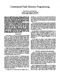
integral part of the on-chip error correction system. (2) TCM can effectively integrate ECC with modulation and achieve significant gain over the conventional design practice that considers ECC and modulation separately. This paper, for the first time, demonstrates the great promise of TCM-based on-chip error correction for code storage ML Flash memory. Using 2bits/cell Flash memory as a test vehicle, we designed TCM-based systems for three scenarios where the protected user data are 16-bit, 32-bit and 64bit, respectively. Compared with the systems using 2-errorcorrecting BCH codes, the TCM-based systems can achieve ∼1 order of magnitude better bit error rate while saving 15.3% (16-bit), 13.0% (32-bit) and 2.6% (64-bit) memory cells, respectively. Cadence and Synopsys tools with 0.18µm CMOS technology were used to implement the read datapath including sensing circuits and TCM demodulation and decoding circuits. The latency and silicon area are 12.3ns and 0.118mm2 (16-bit), 30.3ns and 0.156 mm2 (32-bit), and 66.3ns and 0.196mm2 (64-bit), respectively. 2. TCM SYSTEM STRUCTURE The basic idea of TCM is to jointly design trellis codes (i.e., convolutional codes) and signal-mapping (i.e., modulation) processes to maximize the free Euclidean distance1 between coded signal sequences. As illustrated in Fig. 1, given an l-level/cell memory core, an m-dimensional TCM encoder receives a sequence of n-bit input data and generates a sequence of (n+r)-bit data, where each (n+r)-bit data are stored in m memory cells and 2n+r ≤ lm . The encoding process can be outlined as follows: (1) A convolutional encoder convolves the input k bits sequence with r linear algebraic functions and generates k+r coded bits. (2) Each k+r coded bits select one of the 2k+r subsets of an m-D signal constellation, where each subset contains 2n−k signal points. (3) The additional n-k uncoded bits select an individual m-D signal point from the selected subset. Let s denote the memory order of the convolutional code 1 Similar to the Hamming distance of linear block codes, free Euclidean distance determines the error correction capability of convolutional codes, i.e., a convolutional code with free Euclidean distance of df ree can correct at least b(df ree − 1)/2c code symbol errors.
Encoder k bits n bits
Decoder
k+r bits
Convolutional code encoder
m-D modulator
m
l-level/cell Flash memory core
m
m-D demodulator
2k+r
Viterbi decoder
n bits
n-k bits
Fig. 1. Block diagram of TCM-based on-chip error correction system. encoder. To protect an N-bit data block, the TCM encoder totally receives N+s bits including s zero bits for convolutional code termination. If N+s is not divisible by n, the last input to the encoder will contain less than n bits, for which the m-D modulation may be simplified to a modulation with a lower dimension. As illustrated in Fig. 1, the TCM decoder contains an m-D demodulator that provides 2k+r branch metrics and branch symbol decisions to the Viterbi decoder for trellis decoding.
3. EFFECTIVENESS OF TCM-BASED ON-CHIP ERROR CORRECTION In this section, we demonstrate the effectiveness of TCMbased on-chip error correction using 2bits/cell Flash memory as a test vehicle. In this work, we use a Flash memory cell threshold voltage distribution model, illustrated in Fig. 2, approximated from the results published in [6]. The two inner distributions have the same variance, denoted as σ. The variances of the two outer distributions are 4σ and 2σ, respectively. Let Vmax denote the voltage difference between the means of the two outer distributions. The locations of the means of the two inner distributions are determined to minimize the raw cell error probability. 0.4 0.35 0.3 0.25 0.2 0.15
Vmax
0.1 0.05 0 −10
−5
0
5
10
15
20
25
30
35
40
Fig. 2. The approximate Flash memory cell threshold voltage distribution model.
3.1. System Design and Performance Evaluation We designed three TCM-based systems that protect 16-bit, 32-bit and 64-bit user data in one codeword, respectively. These three systems share the same system design parameters (referred to Fig. 1): n=7, k=2, r=1, m=4, and the memory order of the convolutional code v=3. The signal read from each memory cell is quantized by 12 levels. To realize 4-D modulation, we use the scheme proposed by Wei [7] that hierarchically partitions the 4-D rectangular lattice formed by four memory cells into eight 4-D sub-lattices. Each coded 3-bit word from the convolutional code encoder selects one out of the eight sub-lattices. To protect 16-bit user data, the TCM encoder receives 19 bits (including 3 zero bits for termination) and finishes encoding in three steps: during each of the first two steps, it receives 7 bits and maps the coded 8 bits onto 4 memory cells through 4-D modulation; in the last step, it receives 5 bits and maps the coded 6 bits onto 3 memory cells through 3-D modulation that is obtained by collapsing one 2-D constellation in the original 4-D modulation into a 1-D constellation. Therefore, this system is denoted as (11,8) TCM, i.e., one codeword occupies 11 memory cells and protects 2×8=16-bit user data (notice that each memory cell stores 2 bits). For the purpose of comparison, we considered two other ECC schemes using linear block codes: (i) a (11,8,1) 4-ary shortened Hamming code; (ii) a (13,8,2) 4-ary shortened 2-error-correcting BCH code. Fig. 3(a) shows the performance comparison of these three schemes. Although the performance curves of the two linear block codes can be analytically derived, we have to rely on extensive computer simulation to obtain the performance curve of the (11,8) TCM system, for which the solid part is obtained by computer simulation and the dashed part is estimated following the trend of the simulation results. With the same coding redundancy, (11,8) TCM can achieve about five orders of magnitude better performance than (11,8,1) Hamming code. Compared with (13,8,2) BCH code, (11,8) TCM can achieve almost the same performance while realizing a saving of 2/13 (15.4%) memory cells. To protect 32-bit user data, the TCM encoder receives 35 bits and finishes encoding in 5 steps, each step maps 8 bits onto 4 memory cells through 4-D modulation. Hence,
0
0
10
−2
10
10
−4
10
−4
−4
−8
10
BER
−6
10
−6
10
−8
10
−10
15
10
−10
−10
10
−12
10
−12
20
25
V
30
/σ
35
40
45
10
−6
10
−8
10
10
Uncoded (36,32,1) Hamming (39,32,2) BCH (38,32) TCM
−2
10
BER
BER
10
Uncoded (19,16,1) Hamming (23,16,2) BCH (20,16) TCM
−2
10
10
0
10
Uncoded (11,8,1) Hamming (13,8,2) BCH (11,8) TCM
15
−12
20
25
max
V
30
/σ
35
40
45
10
15
20
max
25
V
30
/σ
35
40
45
max
Fig. 3. BER performance when protecting 16-bit, 32-bit and 64-bit user data (In TCM schemes, the signal read from each memory cell is quantized by 12 levels). this is denoted as (20,16) TCM, i.e., one codeword occupies 20 memory cells and protects 32-bit user data. The (20.16) TCM is compared with two linear block codes: (i) a (19,16,1) 4-ary shortened Hamming code; (ii) a (23,16,2) 4ary shortened BCH code. Fig. 3(b) shows their performance comparison. To protect 64-bit user data, the TCM encoder receives 67 bits and finishes encoding in 10 steps: during each of the first 9 steps, it receives 7 bits and maps the coded 8 bits onto 4 memory cells through 4-D modulation; in the last step, it receives 4 bits that bypass the convolutional code encoder and directly map onto 2 memory cells through 2-D modulation that is a constituent of the original 4-D modulation. Hence, this is denoted as (38,32) TCM. We compared it with two linear block codes: (i) a (36,32,1) 4-ary shortened Hamming code; (ii) a (39,32,2) 4-ary shortened BCH code. Fig. 3(c) shows their performance comparison. Table 1 summarizes the comparison between the TCM and the other ECC schemes discussed above in terms of coding redundancy and error-correcting performance.
Table 1. Comparison between TCM and the other ECC schemes based on linear block code. Savings Performance TCM Competing ECC of cells gain (11,8,1) Hamming 0 ∼ 105 (11,8) (13,8,2) BCH 15.4% ∼1 (19,16,1) Hamming -5.3% ∼ 105 (20,16) (23,16,2) BCH 13% ∼ 10 (36,32,1) Hamming -5.6% > 105 (38,32) (39,32,2) BCH 2.6% > 10
3.2. Silicon Implementation The above shows the effectiveness of TCM-based on-chip error correction in terms of coding redundancy and errorcorrecting performance. However, to be a promising candidate for ML Flash memory, it should be able to achieve small latency and negligible silicon area compared with the overall memory die size. In the following, we present proofof-concept implementation results for the above three TCMbased systems for protecting 16-bit, 32-bit, and 64-bit user data. Clearly, TCM encoders are very simple and can easily achieve very small latency with negligible silicon cost. Hence we will only focus on TCM decoders. The TCM decoding datapath contains higher precision sensing circuits, 4-D demodulator, and Viterbi decoder. The sensing circuit realizes 12-level quantization, instead of 4level quantization as in the conventional linear block code based ECC scheme. Using Cadence tool with IBM 0.18µm 7WL technology, we designed a current-mode 12-level parallel sensing circuit following the structure proposed in [8]. Fig. 4 shows the general structure of a 12-level currentmode parallel sensing circuit that mainly contains eleven current comparators. 12-level quantization is realized by comparing the current from the selected memory cell with the reference currents from the eleven reference cells which are appropriately programmed. The silicon area of one 12level current-mode parallel sensing circuit is estimated as 0.006mm2 . The simulation results show that the worst-case sensing latency (i.e., the input current is equal to one of the reference currents) is about 300ps. Upon receiving the data from four 12-level sensing circuits, the 4-D demodulator finds the most likely point in each 4-D signal subset and calculates the corresponding loglikelihood metric as the branch metrics sent to the Viterbi decoder. Leveraging the hierarchical structure inherent in the 4-D modulation, the 4-D demodulator has a data flow
COMP11
Ic
COMP2
- +
Ic
COMP1
- +
Ic
Table 2. Summary of implementation metrics.
- +
Current amplication & replicas
(11,8) TCM (20,16) TCM (38,32) TCM
Dummy replicas
Find cloest point in each 1-D subset and its metric
Find cloest point in each 2-D subset and its metric
FindSelected cloest point in each Cell 1-D subset and its metric
Reference Cells Find cloest point in each 4-D subset and its metric
Fig. 4. Structure of a 12-level parallel sensing circuit.
Find cloest point in each 1-D subset and its metric
Find cloest point in each 2-D subset and its metric
Find cloest point in each 1-D subset and its metric
structure as shown in Fig. 5. The output branch metrics are represented with 6 bits. From four 12-level sensing circuits
From four 12-level sensing circuits
2
Find cloest point in each 1-D subset and its metric Find cloest point in each 1-D subset and its metric Find cloest point in each 1-D subset and its metric Find cloest point in each 1-D subset and its metric
Find cloest point in each 2-D subset and its metric
Area (mm2 ) 0.118 0.156 0.196
Latency2 (ns) 12.3 30.3 66.3
Includes latency of sensing circuits and TCM decoding.
design an on-chip error correction system for code storage ML Flash memory. Compared with conventional practice using linear block codes, the TCM-based design solution can provide better coding redundancy vs. error-correcting performance trade-offs. To evaluate the silicon cost of using TCM-based on-chip error correction, we implemented the read datapath consisting of high-precision sensing circuits and TCM decoder with 0.18µm CMOS technology. The results suggest that TCM-based systems can achieve small operational latency and occupy small silicon area. 5. REFERENCES
Find cloest point in each 4-D subset and its metric Find cloest point in each 2-D subset and its metric
Fig. 5. Data flow of the 4-D demodulator. The last block on the decoding datapath is a Viterbi decoder. To minimize the decoding latency, we use stateparallel register-exchange Viterbi decoder architecture. Since Viterbi decoder implementation has been extensively addressed in the open literature, we will not elaborate on the decoder implementation details. Interested readers are referred to [9]. Here we note that, for the scenario of protecting 16-bit user data, since the Viterbi decoder finishes the decoding in only 3 steps, we directly unrolled the recursive datapath of the original Viterbi decoder and fully optimize the circuit’s structure, which reduces both silicon area and decoding latency. Table 2 summarizes the read datapath implementation metrics of the three TCM systems. We note that the TCM systems protecting 32-bit and 64-bit user data contain four sensing circuits and one 4-D demodulator, while the TCM system protecting 16-bit user data contains 11 sensing circuits and two 4-D and one 3-D demodulators in order to match the parallelism of the unrolled Viterbi decoder. 4. CONCLUSIONS Leveraging the non-trivial modulation process of ML memory, this paper, for the first time, applies the TCM concept to
[1] B. Ricco et al., “Nonvolatile multilevel memories for digital applications,” Proceedings of the IEEE, vol. 86, pp. 2399– 2423, Dec. 1998. [2] S. Gregori, A. Cabrini, O. Khouri, and G. Torelli, “On-chip error correcting techniques for new-generation Flash memories,” Proceedings of the IEEE, vol. 91, pp. 602–616, April 2003. [3] A. Silvagni, G. Fusillo, R. Ravasio, M. Picca, and S. Zanardi, “An overview of logic architectures inside Flash memory devices,” Proceedings of the IEEE, vol. 91, pp. 569–580, April 2003. [4] D. Rossi, C. Metra, and B. Ricco, “Fast and compact error correcting scheme for reliable multilevel Flash memories,” in Proc. of the Eighth IEEE International On-Line Testing Workshop, July 2002, pp. 221–225. [5] G. Ungerboeck, “Trellis-coded modulation with redundant signal sets Part I, II,” IEEE Communications Magazine, vol. 25, pp. 5–21, Feb. 1987. [6] G. Atwood, A. Fazio, D. Mills, and B. Reaves, “Intel strataflashT M memory technology overview,” Intel Technology Journal, pp. 1–8, 4th Quarter 1997. [7] L. F. Wei, “Trellis-coded modulation with multidimensional constellations,” IEEE Transactions on Information Theory, vol. 33, pp. 483–501, July 1987. [8] C. Calligaro, R. Gastaldi, A. Manstretta, and G. Torelli, “A high-speed parallel sensing scheme for multi-level nonvolatile memories,” in Proc. of International Workshop on Memory Technology, Design and Testing, Aug. 1997, pp. 96– 101. [9] G. Fettweis and H. Meyr, “High-speed parallel Viterbi decoding: algorithm and VLSI-architecture,” IEEE Communications Magazine, vol. 29, pp. 46–55, May 1991.